Demonstration of Fin-Tunnel Field-Effect Transistor with Elevated Drain


1
Inter-university Semiconductor Research Center, Department of Electrical and with the Department of Computer Engineering, Seoul National University, Seoul 151-744, Korea
2
Department of Electrical and with the Department of Computer Engineering, Seoul National University, Seoul 151-744, Korea
3
Department of Electrical and Computer Engineering, Ajou University, Suwon 16944, Korea
*
Authors to whom correspondence should be addressed.
Micromachines 2019, 10(1), 30; https://doi.org/10.3390/mi10010030
Submission received: 22 November 2018
/
Revised: 20 December 2018
/
Accepted: 4 January 2019
/
Published: 7 January 2019
(This article belongs to the Special Issue Extremely-Low-Power Devices and Their Applications)
Abstract
:In this paper, a novel tunnel field-effect transistor (TFET) has been demonstrated. The proposed TFET features a SiGe channel, a fin structure and an elevated drain to improve its electrical performance. As a result, it shows high-level ON-state current (ION) and low-level OFF-state current (IOFF); ambipolar current (IAMB). In detail, its ION is enhanced by 24 times more than that of Si control group and by 6 times more than of SiGe control group. The IAMB can be reduced by up to 900 times compared with the SiGe control group. In addition, technology computer-aided design (TCAD) simulation is performed to optimize electrical performance. Then, the benchmarking of ON/OFF current is also discussed with other research group’s results.
1. Introduction
Numerous studies about tunnel field-effect transistor (TFET) have been performed by several research groups as a promising device for an ultra-low power operation [1,2,3,4]. In case of metal-oxide-semiconductor FETs (MOSFETs), there exist a theoretical limit of 60 mV/dec subthreshold swing (SS) at 300 K-temperature because their carrier injection is based on the thermionic emission [5,6]. On the other hand, TFETs are relatively independent to the Boltzmann distribution since the function tail is removed by forbidden gap and the band-to-band tunneling (BTBT) dominates the carrier injection from source to channel [7,8]. Thus, the SS can be reduced to less than 60 mV/dec at RT, which allows the supply voltage (VDD) to be decreased drastically, maintaining high ON-state current (ION). In addition, its fabrication process is highly compatible with that of MOSFETs. In spite of these advantages, however, the TFETs have some technical issues to be employed for a real application. First, it suffers from low-level ON-state current which is mainly attributed to the high tunnel resistance at source-to-channel junction [9,10,11]. In order to solve this, the Ge material has been adopted for its low bandgap and direct BTBT tunneling [12]. However, It is difficult to make a heterojunction using Ge material [12]. Second, a BTBT at channel-to-drain junction increases OFF-state leakage current (IOFF); ambipolar current (IAMB). Since these issues degrade TFET circuit’s electrical performance such as operation speed and power consumption, they should be addressed [13,14,15,16].
The purpose of this paper is to demonstrate a novel TFET which achieves larger ION and smaller IAMB than that of conventional Si TFETs. As shown in Figure 1, the proposed TFET features a fin channel structure for improved gate controllability and a SiGe channel for higher ION as reducing tunnel resistance. In addition, in the proposed TFET, IAMB can be suppressed with the help of relatively large Si band gap at drain. In addition, its feasibility for better performance is examined by technology computer-aided design (TCAD) simulation. Last of all, based on the measurement and optimized results, the benchmarking of ON/OFF current ratio (ION/IOFF) and SS with the state-of-the-art TFETs is also discussed.
2. Device Fabrication
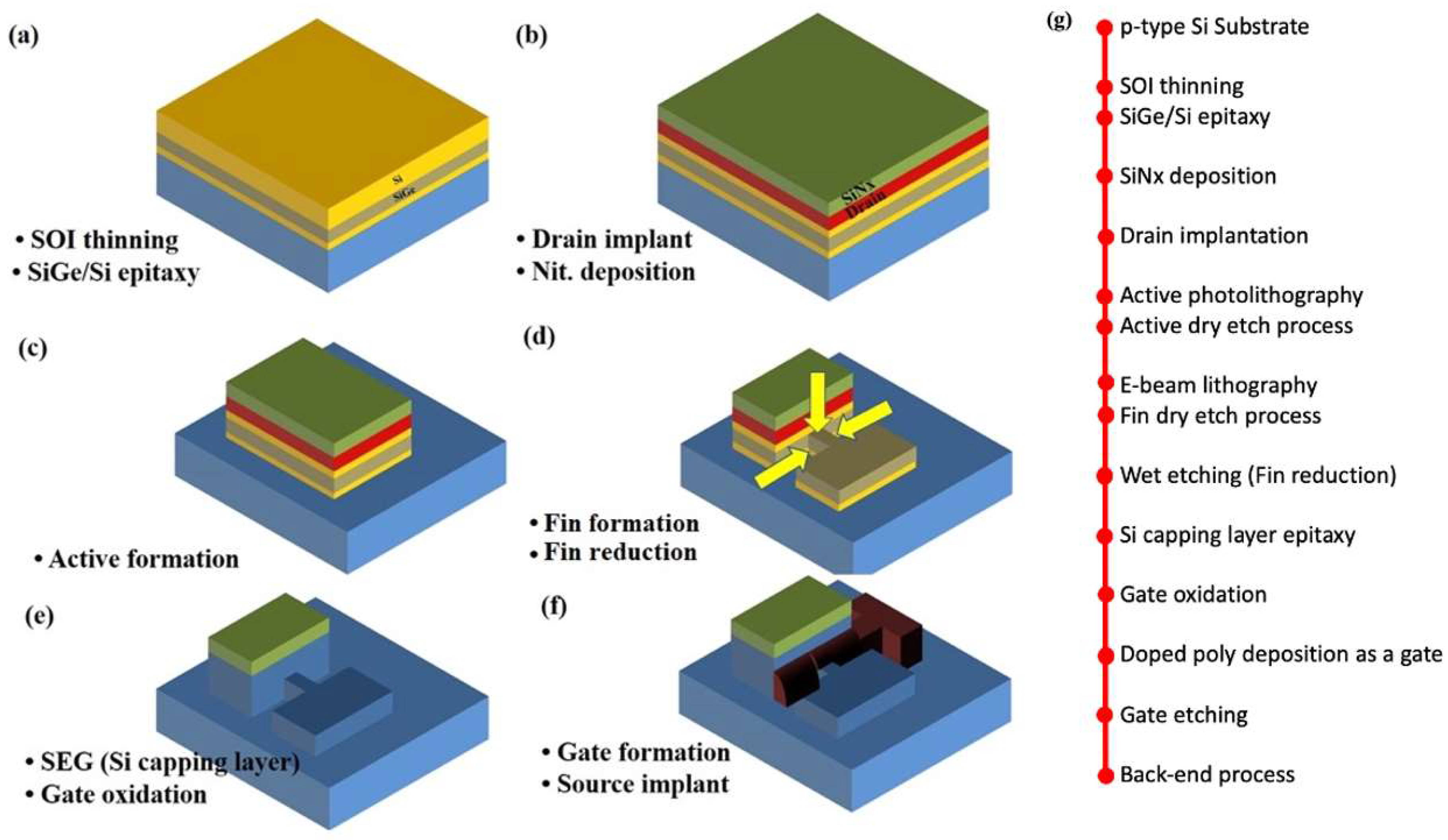
The key process steps for the proposed TFETs are described in Figure 2a First, silicon-on-insulator (SOI) thickness is decreased by using wet oxidation followed by SiO2 wet etching. Then, SiGe and Si layers are grown on the SOI substrate by metal organic chemical vapor deposition (MOCVD). The process condition is as follow: a gas mixture of H2 at 20 sccm, SiH4 at 20 sccm, and GeH4 at 90 sccm is used at 670 °C during 61 s for 300 Å-thick SiGe. Auger electron spectroscope (AES) and transmission electron microscope (TEM) image confirm a single crystalline Si0.7Ge0.3 is well grown on Si substrate (Figure 3) As ion implantation is performed at 10 keV-acceleration energy, 7°-tilted angle and 8 × 10¹⁴ ions/cm2-dose. Then, SiNx is deposited by plasma-enhanced CVD (PECVD) as an etching mask during an active patterning (c). PECVD nitride is adopted since it is low temperature process with 400 °C and 20 s, in which the implanted dopants in the drain region can rarely diffuse. (d) Some part of Si on active regions are removed by photolithography and reactive ion etching (RIE) processes forming SiGe source and channel while the remaining Si on mesa becomes raised drain region. In case of channel, an additional patterning is conducted by mix-and-match process of e-beam lithography and photolithography to form 50 nm-width active fin (Figure 2d and Figure 4).
The SiGe/Si fin width is further reduced by standard cleaning-1 (SC-1) solution which consists of ammonium hydroxide (NH4OH), hydrogen peroxide (H2O2), and de-ionized wafer (H2O) [17,18]. The NH4OH:H2O2:H2O ratio is 1:8:64 in which the etching rate of the SiGe is ~0.85 nm/min. After 13 min process in the SC-1 solution, the SiGe fin width is reduced to 39.5 nm as shown in the inset of Figure 4. As shown in Figure 2e, an 1 nm-thick Si capping layer is deposited by selective epitaxy growth (SEG) followed by dry oxidation for a gate dielectric. It has been demonstrated that this process can efficiently prevent defects which could be induced between SiO2 and SiGe [19]. The capacitance equivalent thickness (CET) of gate dielectric is confirmed as 3.4 nm from the capacitance-voltage (C-V) curve shown in Figure 5. (f) For a short-channel gate, sidewall spacer technique is applied: n-type doped polycrystalline-Si (poly-Si) is deposited by low pressure CVD (LPCVD) and etched by Si RIE process after photolithography for a gate pad. As a result, ~76 nm-length gate is defined self-aligning to the drain (Figure 6). After that, BF2 implantation with 10 keV-acceleration energy, 7°-tilted angle and 8 × 10¹⁴ ions/cm2-dose is performed for a source region. The dopant activation is performed by rapid thermal process (RTP) with 900 °C and 5 s. Note that all processes for gate, source and drain formation are self-aligned to each other and can be compatible with state-of-the-art ultra-short channel technology. Finally, as a back-end-of line (BEOL), high plasma density (HDP) oxide is deposited as an interlayer dielectric (ILD) and metal layers (Ti/TiN/Al/TiN stacks) are deposited by physical vapor deposition (PVD) after contact formation. (g) Then, all of processes are summarized in the flow graph.
For the control samples, the planar Si and SiGe TFETs were fabricated. In the case of SiGe TFET, Si0.7Ge0.3 layers with a thickness of 30 nm are grown on SOI (100) substrates. The SOI layer is lightly p-doped (1 × 1015 cm−3) with a thickness of 70 nm. For additional comparison, the Si TFET is fabricated on a 100 nm-thick SOI wafer. The gate stack consists of 200 nm poly-Si layer and 3 nm SiO2. After gate patterning, source and drain region are defined through photolithography and ion implantation processes. The ion implantation and BEOL processes are same with the processes in proposed TFET.
3. Measurement and Results
Figure 7a shows the transfer characteristics of the proposed device with the various drain voltages (VDSs). The SS is extracted at VDS of 0.1 V and a turn-ON voltage (Vturn-ON) is defined as gate voltages (VGS) where BTBT first occurs. The IOFF and ION are extracted when VGS is Vturn-ON and gate overdrive (VOV = VGS − Vturn-ON) is equal to 2 V, respectively. The minimum SS is 81 mV/dec and ION/IOFF is 2.8 × 10⁴. Figure 7b shows the output characteristics of the proposed TFET with the various VGSs. Note that, the conventional planar devices suffer from short channel effect (SCE) due to their weak gate controllability over the channel [20,21]. Generally, the SCE can be confirmed with drain induced current enhancement (DICE) in transfe curves and increase of saturation current in output characteristics. According to the measured results, however, there is no obvious SCE in the proposed TFET as shown in Figure 7a,b.
The proposed TFET’s electrical characteristics are compared with that for planar Si and SiGe TFETs as control groups. Figure 8 shows the transfer characteristics of both groups at 1.0 V-VDS. The SS and ION, IAMB and ION/IOFF are extracted from the curves and summarized in Table 1. The proposed TFET shows superior performance than the control ones in the several aspects. First, the SS of proposed device, which is measured at Vturn-ON is 81 mV/dec whereas 151 mV/dec and 87 mV/dec are measured in planar Si and SiGe TFETs, respectively. Second, the proposed TFET shows 139 nA/μm-ION which is 34 times and 5 times bigger than that for Si and SiGe TFETs, respectively. Last of all, the IAMB can be reduced by up to 103 times compared with the SiGe TFET. These results are attributed in part to the SiGe’s narrow bandgap at the source area and in part to the strong gate-to-channel coupling with the help of fin-structured channel [22]. In addition, the elevated drain area reduces the BTBT between the channel and the drain by Si bandgap [23].
The proposed TFET has remarkable electrical characteristics as shown above. However, the IOFF of proposed TFET near zero VGS is higher than that of planar Si TFET (Figure 8). In order to confirm the mechanism precisely, transfer characteristics with various temperature are investigated. As shown in Figure 9, drain current (ID) is relatively independent to the VGS at around 0 V while it increases rapidly as a function of temperature. The result confirms that this current is dominated by Shockley–Read–Hall (SRH) generation–recombination [24].
4. Discussion
The objective of this study is to demonstrate the TFET with high ION and low IAMB. Compared with planar TFETs which is fabricated with the same processes, there is no doubt that the proposed structure is effective to improve electrical performance. However, the measured results imply that it requires further optimization for the better performance than the other strategies [25,26,27,28,29,30,31,32,33,34,35,36,37]. Therefore, the proposed TFET’s feasibility for the better performance is examined by TCAD simulations using Synopsys Sentaurus™. Above all, BTBT parameters in Kane’s tunneling model are calibrated by measured results [17]. In the simulations, to calculate BTBT generation rate (G) per unit volume in the uniform electric field, Kane’s model is used and fitted parameters are as follows (Equation (1)).
where F0 = 1 V/m, P = 2.5 for indirect BTBT. Prefactor A and exponential factor B are the Kane parameters and F is the electric field. Both linear and log scale simulated transfer characteristics are well matched to experimental data when A: 1 × 1014 cm−1·s−1/B: 3 × 10⁶ V/cm are applied to TFETs. Then, the thickness of the gate dielectric is analyzed. Unlike advanced technologies, the proposed TFET uses 3.4 nm thick SiO2 as the gate dielectric. Thus, if the gate dielectric is adjusted to 1 nm, the proposed TFET can obtain higher ION at the low VGS (Figure 10). Figure 11 compares the ION/IOFF as a function of SS for the device shown in this paper and that in the previous articles [25,26,27,28,29,30,31,32,33,34,35,36,37]. Compared with the other Si based TFETs, the optimized TFET shows a remarkable performance in terms of minimum SS and ION/IOFF.
5. Conclusions
In this paper, a novel TFET with SiGe fin channel and elevated drain has been introduced. The SiGe fin channel included small-bandgap and better electrostatic controllability which are leading high ION and low SS, compared to conventional planar TFETs. Furthermore, the elevated drain could yield lower IAMB due to the increased physical distance between channel and drain. Considering these features, we have examined and demonstrated the fabrication processes of the proposed device. In addition, based on the measured results, the proposed TFET is calibrated by TCAD simulation. In order to optimize the device into state-of-the-art technique, the proposed device with thin gate dielectric is also simulated. The results proved that the device showed the improved ION current and smaller SS. Consequently, these features of the proposed device will be available for compensating the weaknesses of conventional TFETs. Therefore, it will be one of the promising candidates for next-generation devices.
Author Contributions
Writing (original draft preparation, review, and editing), J.H.K. and H.W.K.; Data analysis, G.K.; Supervision, S.K. and B.-G.P.
Funding
This research was supported in part by the Brain Korea 21 Plus Project and in part by the NRF of Korea funded by the Ministry of Education (MOE) under Grant 2017R1D1A1B03034352 (Basic Science Research Program) and in part by the MOTIE/KSRC under Grant 10080575 (Future Semiconductor Device Technology Development Program). The EDA tool was supported by the IC Design Education Center (IDEC), Korea.
Conflicts of Interest
The authors declare no conflict of interest.
References
- Choi, W.Y.; Park, B.G.; Lee, J.D.; Liu, T.J.K. Tunneling field-effect transistors (TFETs) with subthreshold swing (SS) less than 60 mV/dec. IEEE Electron Device Lett. 2007, 28, 743–745. [Google Scholar] [CrossRef]
- Wang, P.Y.; Tsui, B.Y. Band engineering to improve average subthreshold swing by suppressing low electric field band-to-band tunneling with epitaxial tunnel layer tunnel FET structure. IEEE Trans. Nanotechnol. 2016, 15, 74–79. [Google Scholar] [CrossRef]
- Kim, S.W.; Choi, W.Y.; Kim, H.; Sun, M.C.; Kim, H.W.; Park, B.G. Investigation on hump effects of L-shaped tunneling filed-effect transistors. In Proceedings of the Silicon Nanoelectronics Workshop (SNW), Honolulu, HI, USA, 10–11 June 2012; pp. 1–2. [Google Scholar] [CrossRef]
- Mishra, A.; Pattanaik, M.; Sharma, V. Double gate vertical tunnel FET for hybrid CMOS-TFET based low standby power logic circuits. In Proceedings of the Emerging Research Areas and 2013 International Conference on Microelectronics, Communications and Renewable Energy (AICERA/ICMiCR), 2013 Annual International Conference, Kanjirapally, India, 4–6 June 2013; pp. 1–4. [Google Scholar] [CrossRef]
- Knoch, J. Nanowire Tunneling Field-Effect Transistors. Semicond. Semimet. 2016, 94, 273–295. [Google Scholar] [CrossRef]
- Long, P.; Wilson, E.; Huang, J.Z.; Klimeck, G.; Rodwell, M.J.; Povolotskyi, M. Design and simulation of GaSb/InAs 2D transmissionenhanced tunneling FETs. IEEE Electron Device Lett. 2016, 37, 107–110. [Google Scholar] [CrossRef]
- Sun, S.W.; Tsui, P.G. Limitation of CMOS supply-voltage scaling by MOSFET threshold-voltage variation. IEEE J. Solid-State Circuits 1995, 30, 947–949. [Google Scholar] [CrossRef]
- Frank, D.J.; Dennard, R.H.; Nowak, E.; Solomon, P.M.; Taur, Y.; Wong, H.S.P. Device scaling limits of Si MOSFETs and their application dependencies. Proc. IEEE 2001, 89, 259–288. [Google Scholar] [CrossRef]
- Kim, S.W.; Kim, J.H.; Liu, T.J.K.; Choi, W.Y.; Park, B.G. Demonstration of L-shaped tunnel field-effect transistors. IEEE Trans. Electron Devices 2016, 63, 1774–1778. [Google Scholar] [CrossRef]
- Leonelli, D.; Vandooren, A.; Rooyackers, R.; Verhulst, A.S.; De Gendt, S.; Heyns, M.M.; Groeseneken, G. Performance enhancement in multi gate tunneling field effect transistors by scaling the fin-width. Jpn. J. Appl. Phys. 2010, 49, 04DC10. [Google Scholar] [CrossRef]
- Gandhi, R.; Chen, Z.; Singh, N.; Banerjee, K.; Lee, S. CMOS-Compatible Vertical-Silicon-Nanowire Gate-All-Around p-Type Tunneling FETs With ≤ 50-mV/decade Subthreshold Swing. IEEE Electron Device Lett. 2011, 32, 1504–1506. [Google Scholar] [CrossRef]
- Kim, S.W.; Choi, W.Y. Hump Effects of Germanium/Silicon Heterojunction Tunnel Field-Effect Transistors. IEEE Trans. Electron Devices 2016, 63, 2583–2588. [Google Scholar] [CrossRef]
- Verhulst, A.S.; Vandenberghe, W.G.; Maex, K.; Groeseneken, G. Tunnel field-effect transistor without gate-drain overlap. Appl. Phys. Lett. 2007, 91, 053102. [Google Scholar] [CrossRef]
- Anghel, C.; Chilagani, P.; Amara, A.; Vladimirescu, A. Tunnel field effect transistor with increased ON current, low-k spacer and high-k dielectric. Appl. Phys. Lett. 2010, 96, 122104. [Google Scholar] [CrossRef]
- Anghel, C.; Gupta, A.; Amara, A.; Vladimirescu, A. 30-nm tunnel FET with improved performance and reduced ambipolar current. IEEE Trans. Electron Devices 2011, 58, 1649–1654. [Google Scholar] [CrossRef]
- Narang, R.; Saxena, M.; Gupta, R.S.; Gupta, M. Assessment of ambipolar behavior of a tunnel FET and influence of structural modifications. J. Semicond. Technol. Sci. 2012, 12, 482–491. [Google Scholar] [CrossRef]
- Kobayashi, H.; Ryuta, J.; Shingyouji, T.; Shimanuki, Y. Study of Si etch rate in various composition of SC1 solution. Jpn. J. Appl. Phys. 1992, 32, L45. [Google Scholar] [CrossRef]
- Sun, M.C.; Kim, G.; Lee, J.H.; Kim, H.; Kim, S.W.; Kim, H.W.; Lee, J.-H.; Shin, H.; Park, B.G. Patterning of Si nanowire array with electron beam lithography for sub-22 nm Si nanoelectronics technology. Microelectron. Eng. 2013, 110, 141–146. [Google Scholar] [CrossRef]
- Palmer, M.J.; Braithwaite, G.; Grasby, T.J.; Phillips, P.J.; Prest, M.J.; Parker, E.H.C.; Whall, T.E. Effective mobilities in pseudomorphic Si/SiGe/Si p-channel metal-oxide-semiconductor field-effect transistors with thin silicon capping layers. Appl. Phys. Lett. 2001, 78, 1424–1426. [Google Scholar] [CrossRef] [Green Version]
- Kim, M.; Wakabayashi, Y.; Nakane, R.; Yokoyama, M.; Takenaka, M.; Takagi, S. High Ion/Ioff Ge-source ultrathin body strained-SOI tunnel FETs. In Proceedings of the 2014 IEEE International Electron Devices Meeting (IEDM), San Francisco, CA, USA, 15–17 December 2014; pp. 1–4. [Google Scholar] [CrossRef]
- Zhang, J.; De Marchi, M.; Gaillardon, P.E.; De Micheli, G. A Schottky-barrier silicon FinFET with 6.0 mV/dec subthreshold slope over 5 decades of current. In Proceedings of the 2014 IEEE International Electron Devices Meeting (IEDM), San Francisco, CA, USA, 15–17 December 2014; pp. 1–4. [Google Scholar] [CrossRef]
- Jain, P.; Rastogi, P.; Yadav, C.; Agarwal, A.; Chauhan, Y.S. Band-to-band tunneling in Γ valley for Ge source lateral tunnel field effect transistor: Thickness scaling. J. Appl. Phys. 2017, 122, 014502. [Google Scholar] [CrossRef]
- Kim, H.W.; Kim, J.H.; Kim, S.W.; Sun, M.C.; Park, E.; Park, B.G. Tunneling field-effect transistor with Si/SiGe material for high current drivability. Jpn. J. Appl. Phys. 2014, 53, 06JE12. [Google Scholar] [CrossRef]
- Mookerjea, S.; Mohata, D.; Mayer, T.; Narayanan, V.; Datta, S. Temperature-Dependent I–V Characteristics of a Vertical In0.53Ga0.47As Tunnel FET. IEEE Electron Device Lett. 2010, 31, 564–566. [Google Scholar] [CrossRef]
- Jeon, K.; Loh, W.Y.; Patel, P.; Kang, C.Y.; Oh, J.; Bowonder, A.; Park, C.; Park, C.S.; Smith, C.; Majhi, P.; et al. Si tunnel transistors with a novel silicided source and 46mV/dec swing. In Proceedings of the 2010 symposium on VLSI technology (VLSIT), Honolulu, HI, USA, 15–17 June 2010; pp. 121–122. [Google Scholar] [CrossRef]
- Chang, H.Y.; Adams, B.; Chien, P.Y.; Li, J.; Woo, J.C. Improved subthreshold and output characteristics of source-pocket Si tunnel FET by the application of laser annealing. IEEE Trans. Electron Devices 2013, 60, 92–96. [Google Scholar] [CrossRef]
- Leonelli, D.; Vandooren, A.; Rooyackers, R.; Verhulst, A.S.; Huyghebaert, C.; De Gendt, S.; Heyns, M.M.; Groeseneken, G. Novel architecture to boost the vertical tunneling in tunnel field effect transistors. In Proceedings of the 2011 IEEE International SOI Conference (SOI), Tempe, AZ, USA, 3–6 October 2011; pp. 1–2. [Google Scholar] [CrossRef]
- Mayer, F.; Le Royer, C.; Damlencourt, J.F.; Romanjek, K.; Andrieu, F.; Tabone, C.; Previtali, B.; Deleonibus, S. Impact of SOI, Si1-x GexOI and GeOI substrates on CMOS compatible tunnel FET performance. In Proceedings of the 2008 IEEE International Electron Devices Meeting (IEDM), San Francisco, CA, USA, 15–17 December 2008; pp. 1–5. [Google Scholar] [CrossRef]
- Moselund, K.E.; Bjork, M.T.; Schmid, H.; Ghoneim, H.; Karg, S.; Lortscher, E.; Riess, W.; Riel, H. Silicon nanowire tunnel FETs: Low-temperature operation and influence of high-κ gate dielectric. IEEE Trans. Electron Devices 2011, 58, 2911–2916. [Google Scholar] [CrossRef]
- Gandhi, R.; Chen, Z.X.; Singh, N.; Banerjee, K.; Lee, S.J. Vertical Si-nanowire n-type tunneling FETs with low subthreshold swing (≤50 mV/decade) at room temperature. IEEE Electron Device Lett. 2011, 32, 437–439. [Google Scholar] [CrossRef]
- Walke, A.M.; Vandooren, A.; Rooyackers, R.; Leonelli, D.; Hikavyy, A.; Loo, R.; Verhulst, A.S.; Kao, K.-H.; Huyghebaert, C.; Groeseneken, G.; et al. Fabrication and Analysis of a Si/Si0.55Ge0.45 Heterojunction Line Tunnel FET. IEEE Trans. Electron Devices 2014, 61, 707–715. [Google Scholar] [CrossRef]
- Chen, Y.H.; Yen, L.C.; Chang, T.S.; Chiang, T.Y.; Kuo, P.Y.; Chao, T.S. Low-temperature polycrystalline-silicon tunneling thin-film transistors with MILC. IEEE Electron Device Lett. 2013, 34, 1017–1019. [Google Scholar] [CrossRef]
- Kim, S.H.; Kam, H.; Hu, C.; Liu, T.J.K. Germanium-source tunnel field effect transistors with record high ION/IOFF. In Proceedings of the 2009 Symposium on VLSI Technology, Honolulu, HI, USA, 16–18 June 2009; pp. 178–179. [Google Scholar]
- Morita, Y.; Mori, T.; Migita, S.; Mizubayashi, W.; Tanabe, A.; Fukuda, K.; Matsukawa, T.; Endo, K.; O’uchi, S.; Liu, Y.X.; et al. Synthetic electric field tunnel FETs: Drain current multiplication demonstrated by wrapped gate electrode around ultrathin epitaxial channel. In Proceedings of the 2013 Symposium on VLSI Technology (VLSIT), Kyoto, Japan, 11–13 June 2013; pp. T236–T237. [Google Scholar]
- Morita, Y.; Mori, T.; Migita, S.; Mizubayashi, W.; Tanabe, A.; Fukuda, K.; Matsukawa, T.; Endo, K.; O’uchi, S.; Liu, Y.X.; et al. Performance enhancement of tunnel field-effect transistors by synthetic electric field effect. IEEE Electron Device Lett. 2014, 35, 792–794. [Google Scholar] [CrossRef]
- Villalon, A.; Le Royer, C.; Nguyen, P.; Barraud, S.; Glowacki, F.; Revelant, A.; Selmi, L.; Cristoloveanu, S.; Tosti, L.; Vizioz, C.; et al. First demonstration of strained SiGe nanowires TFETs with ION beyond 700µA/µm. In Proceedings of the 2014 Symposium on VLSI Technology (VLSI-Technology): Digest of Technical Papers, Honolulu, HI, USA, 9–12 June 2014; pp. 1–2. [Google Scholar] [CrossRef]
- Villalon, A.; Le Royer, C.; Cassé, M.; Cooper, D.; Prévitali, B.; Tabone, C.; Hartmann, J.-M.; Perreau, P.; Rivallin, P.; Damlencourt, J.-F.; et al. Strained tunnel FETs with record I ON: First demonstration of ETSOI TFETs with SiGe channel and RSD. In Proceedings of the 2012 Symposium on VLSI technology (VLSIT), Honolulu, HI, USA, 12–14 June 2012; pp. 49–50. [Google Scholar] [CrossRef]
Figure 1.
Structure of the proposed TFET. It is featured that SiGe fin structure with elevated drain region.
Figure 1.
Structure of the proposed TFET. It is featured that SiGe fin structure with elevated drain region.

Figure 2.
Fabrication process flow of the proposed TFETs. The flow graph summarize all the fabrication process briefly.
Figure 2.
Fabrication process flow of the proposed TFETs. The flow graph summarize all the fabrication process briefly.

Figure 3.
Auger electron spectroscopy (AES). The SiGe layer contains 30% Ge.

Figure 4.
Cross-sectional view of scanning electron microscope (SEM) image which demonstrates Si fin etching. The inset shows top view of SEM image after fin etching and SC-1 reduction processes.
Figure 4.
Cross-sectional view of scanning electron microscope (SEM) image which demonstrates Si fin etching. The inset shows top view of SEM image after fin etching and SC-1 reduction processes.

Figure 5.
Measured C-V curves of MOS capacitors. The measured CET is 3.4 nm.

Figure 6.
Cross-sectional SEM image which demonstrates raised drain and sidewall gate structure. The 76 nm-length gate self-aligning to the drain is well defined.
Figure 6.
Cross-sectional SEM image which demonstrates raised drain and sidewall gate structure. The 76 nm-length gate self-aligning to the drain is well defined.

Figure 7.
(a) Transfer and (b) output characteristics of proposed TFET.

Figure 8.
Transfer characteristics of the proposed TFET and conventional planar TFETs with Si and SiGe channels.
Figure 8.
Transfer characteristics of the proposed TFET and conventional planar TFETs with Si and SiGe channels.

Figure 9.
Transfer characteristics of the proposed TFET in the range of 298–348 K.

Figure 10.
Transfer characteristics of the proposed TFETs with various CET.

Figure 11.
Performance comparison of TFETs. ION/IOFF of TFETs as a function.


Table 1.
Summary of extracted parameters.
| Si TFET | SiGe TFET | Propose TFET | |
|---|---|---|---|
| SS (VDS = 0.1 V) | 151 mV/dec | 87 mV/dec | 81 mV/dec |
| ION | 4 nA/μm | 21 nA/μm | 139 nA/μm |
| IAMB | 13 pA/μm | 16 nA/μm | 18 pA/μm |
| ION/IOFF | 4 × 10³ | 2.7 × 10³ | 2.8 × 10⁴ |
© 2019 by the authors. Licensee MDPI, Basel, Switzerland. This article is an open access article distributed under the terms and conditions of the Creative Commons Attribution (CC BY) license (http://creativecommons.org/licenses/by/4.0/).
Share and Cite
MDPI and ACS Style
Kim, J.H.; Kim, H.W.; Kim, G.; Kim, S.; Park, B.-G. Demonstration of Fin-Tunnel Field-Effect Transistor with Elevated Drain. Micromachines 2019, 10, 30. https://doi.org/10.3390/mi10010030
AMA Style
Kim JH, Kim HW, Kim G, Kim S, Park B-G. Demonstration of Fin-Tunnel Field-Effect Transistor with Elevated Drain. Micromachines. 2019; 10(1):30. https://doi.org/10.3390/mi10010030
Chicago/Turabian StyleKim, Jang Hyun, Hyun Woo Kim, Garam Kim, Sangwan Kim, and Byung-Gook Park. 2019. "Demonstration of Fin-Tunnel Field-Effect Transistor with Elevated Drain" Micromachines 10, no. 1: 30. https://doi.org/10.3390/mi10010030
Note that from the first issue of 2016, this journal uses article numbers instead of page numbers. See further details here.