Carbon Nanotube Electron Emitter for X-ray Imaging

Abstract
:1. Introduction
2. Experimental Section
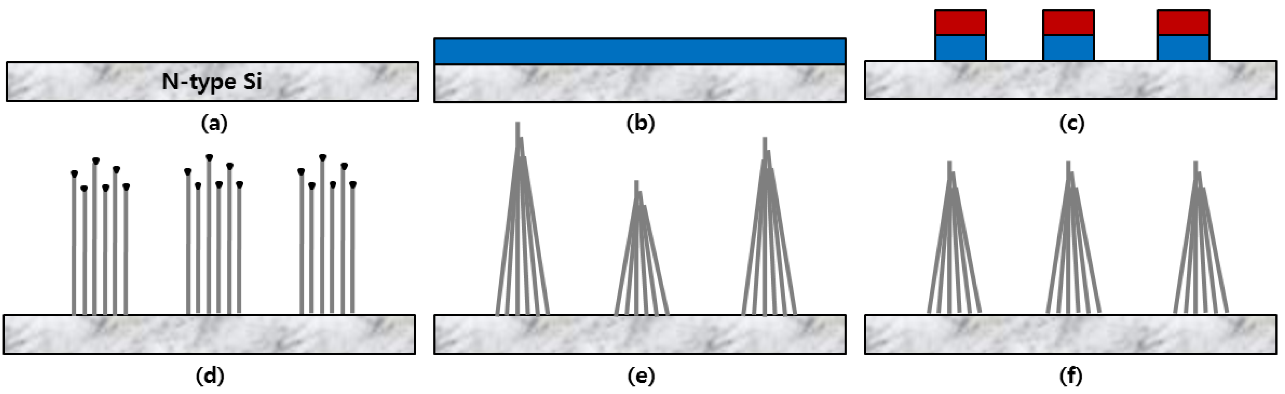
2.1. Growth of Carbon Nanotube for High-Performance Emitters

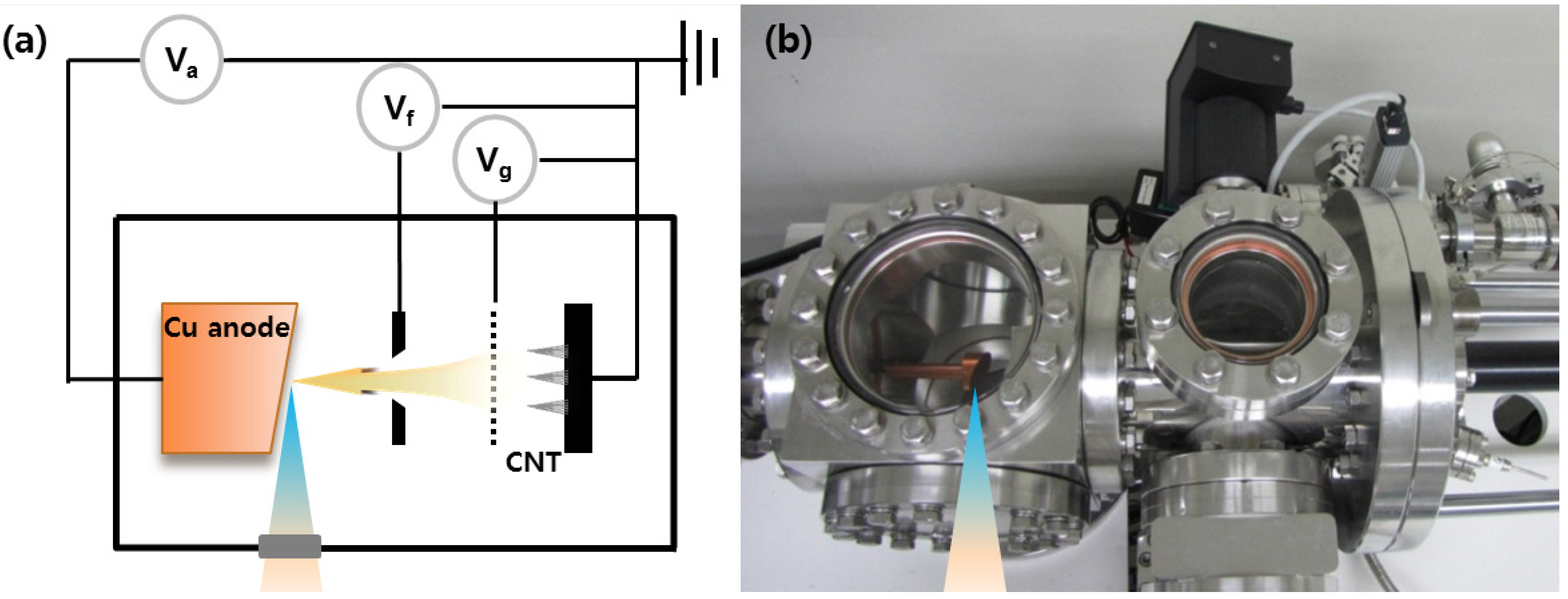
2.2. X-ray Generation with the High-Performance CNT-Emitters

3. Results
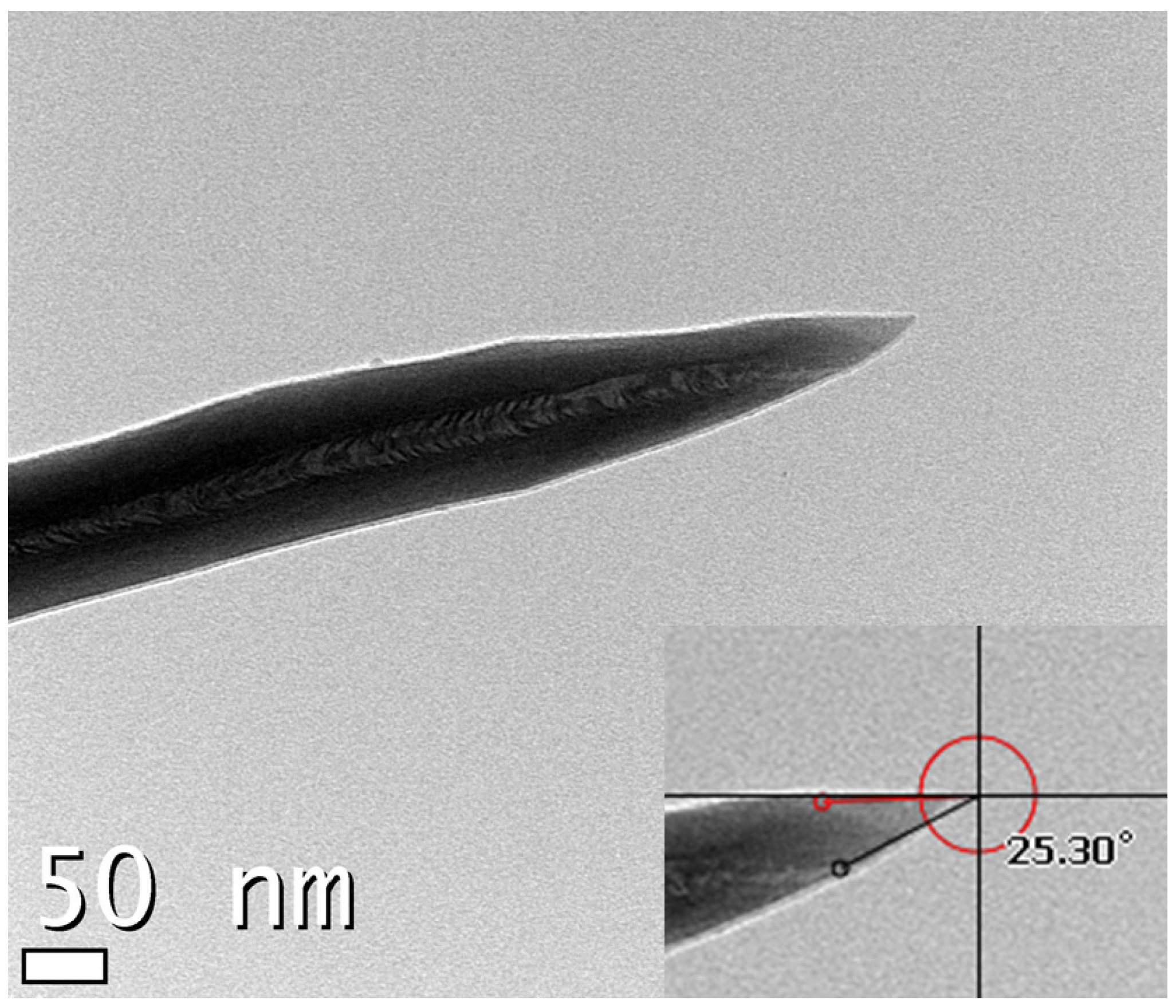
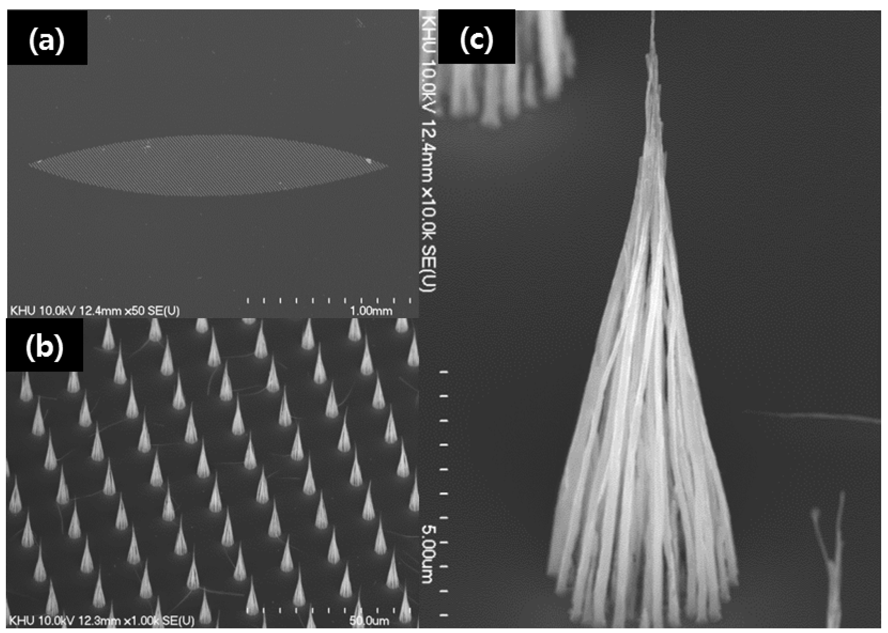
3.1. CNT Emitters for High-Performance X-ray

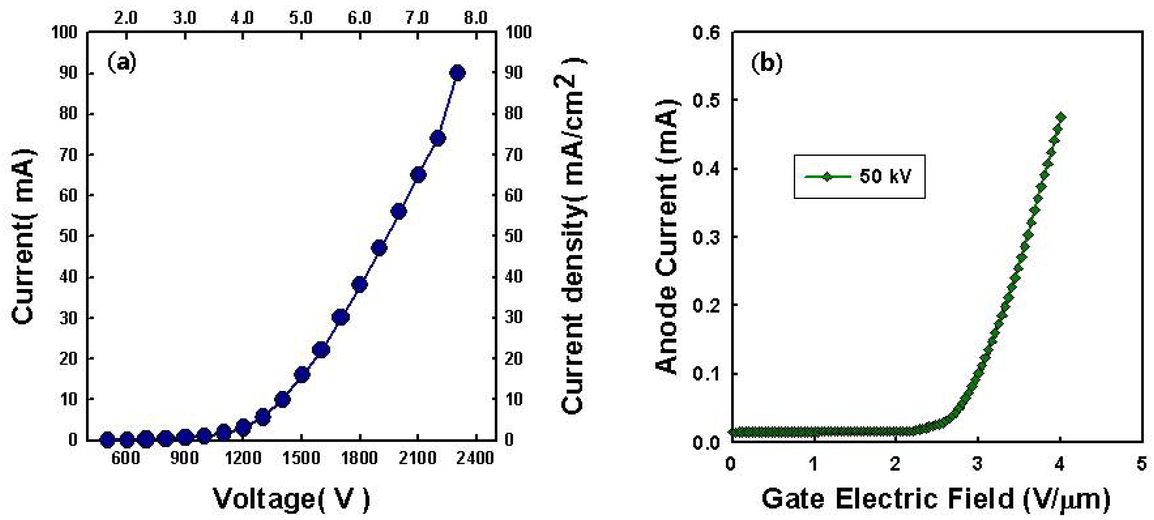
3.2. X-ray Generation with the High-Performance CNT-Emitters


4. Conclusions
Acknowledgments
References
- Baughman, R.H. Carbon nanotubes—The route toward applications. Science 2010, 297, 787–792. [Google Scholar] [CrossRef]
- Wang, S.; Calderon, X.; Peng, R.; Schreiber, E.C.; Zhou, O.; Chang, S. A carbon nanotube field emission multipixel X-ray array source for microradiotherapy application. Appl. Phys. Lett. 2011, 98, 1–4. [Google Scholar]
- van der Snickt, G.; Janssens, K.H.; Dik, J.; de Nolf, W.; Vanmeert, F.; Jaroszewicz, J.; Cotte, M.; Falkenberg, G.; van der Loeff, L. Combined use of synchrotron radiation-based µ-XRF, µ-XRD, µ-XANES and µ-FTIR reveals an alternative degradation pathway of the pigment cadmium yellow (CdS) in a painting by Van Gogh. Anal. Chem. 2012. [Google Scholar] [CrossRef]
- Minoux, E.; Groening, O.; Teo, K.B.; Dalal, S.H.; Gangloff, L.; Schnell, J.P.; Hudanski, L.; Bu, I.Y.; Vincent, P.; Legagneux, P.; Amaratunga, G.A.; Milne, W.I. Achieving high-current carbon nanotube emitters. Nano Lett. 2005, 5, 2135–2138. [Google Scholar] [CrossRef] [PubMed]
- Ascenti, G.; Krauss, B.; Mazziotti, S.; Mileto, A.; Settineri, N.; Vinci, S.; Donato, R.; Gaeta, M. Dual-energy computed tomography (DECT) in renal masses. Acad. Radiol. 2012, 19, 1–8. [Google Scholar] [CrossRef] [PubMed]
- Jung, J.W.; Lee, J.S.; Kwon, S.J.; Park, S.J.; Chang, S.; Kim, J.; Pyo, J.; Kohmura, Y.; Nishino, Y.; Yamamoto, M.; Ishikawa, T.; Je, J.H. Fast microtomography using bright monochromatic X-rays. Rev. Sci. Instrum. 2012, 83, 093704:1–093704:5. [Google Scholar]
- Park, K.; Ryu, J.; Kim, K.; Yu, Y. Growth of carbon nanotubes with resist-assisted patterning process. J. Vac. Sci. Technol. B 2007, 25, 1261–1264. [Google Scholar] [CrossRef]
- Park, K.; Jang, J.; Ryu, J. Field Emission Display and Manufacturing Method of the Same Having Selective Array of Electron Emission Source. US Patent 8,172,633, 8 May 2012. [Google Scholar]
- Kim, K.S.; Ryu, J.H.; Lee, C.S.; Jang, J.; Park, K.C. Enhanced and stable electron emission of carbon nanotube emitter arrays by post-growth hydrofluoric acid treatment. J. Mater. Sci. 2009, 20, 120–124. [Google Scholar]
- Ryu, J.H.; Kim, K.S.; Lee, C.S.; Jang, J.; Park, K.C. Effect of electrical aging on field emission from carbon nanotube field emitter arrays. J. Vac. Sci. Technol. B 2008, 26, 856–859. [Google Scholar] [CrossRef]
- Liu, Z.; Yang, G.; Lee, Y.Z.; Bordelon, D.; Lu, J.; Zhou, O. Carbon nanotube based microfocus field emission X-ray source for microcomputed tomography. Appl. Phys. Lett. 2006, 89, 103–111. [Google Scholar]
- Ryu, J.H.; Bae, N.Y.; Oh, H.M.; Zhou, O.; Jang, J.; Park, K.C. Stabilized electron emission from silicon coated carbon nanotubes for a high-performance electron source. J. Vac. Sci. Technol. B 2011, 29, 02B120:1–02B120:5. [Google Scholar] [CrossRef]
- Nilsson, L.; Groening, O.; Emmenegger, C.; Kuettel, O.; Schaller, E.; Schlapbach, L.; Kind, H.; Bonard, J.; Kern, K. Scanning field emission from patterned carbon nanotube films. Appl. Phys. Lett. 2000, 76, 2071–2073. [Google Scholar] [CrossRef]
© 2012 by the authors; licensee MDPI, Basel, Switzerland. This article is an open access article distributed under the terms and conditions of the Creative Commons Attribution license (http://creativecommons.org/licenses/by/3.0/).
Share and Cite
Ryu, J.H.; Kang, J.S.; Park, K.C. Carbon Nanotube Electron Emitter for X-ray Imaging. Materials 2012, 5, 2353-2359. https://doi.org/10.3390/ma5112353
Ryu JH, Kang JS, Park KC. Carbon Nanotube Electron Emitter for X-ray Imaging. Materials. 2012; 5(11):2353-2359. https://doi.org/10.3390/ma5112353
Chicago/Turabian StyleRyu, Je Hwang, Jung Su Kang, and Kyu Chang Park. 2012. "Carbon Nanotube Electron Emitter for X-ray Imaging" Materials 5, no. 11: 2353-2359. https://doi.org/10.3390/ma5112353
APA StyleRyu, J. H., Kang, J. S., & Park, K. C. (2012). Carbon Nanotube Electron Emitter for X-ray Imaging. Materials, 5(11), 2353-2359. https://doi.org/10.3390/ma5112353