Article

Electrical Performance and Reliability Improvement of Amorphous-Indium-Gallium-Zinc-Oxide Thin-Film Transistors with HfO2 Gate Dielectrics by CF4 Plasma Treatment

1
Department of Electronic Engineering, National Taiwan University of Science and Technology, 43 Section 4, Keelung Road, Taipei 106, Taiwan
2
Graduate Institute of Electro-Optical Engineering, National Taiwan University of Science and Technology, 43 Section 4, Keelung Road, Taipei 106, Taiwan
*
Author to whom correspondence should be addressed.
Materials 2018, 11(5), 824; https://doi.org/10.3390/ma11050824
Submission received: 21 April 2018 / Revised: 9 May 2018 / Accepted: 15 May 2018 / Published: 17 May 2018
(This article belongs to the Special Issue Functional Amorphous Materials)

Abstract

:
In this work, amorphous indium-gallium-zinc oxide thin-film transistors (a-IGZO TFTs) with a HfO2 gate insulator and CF4 plasma treatment was demonstrated for the first time. Through the plasma treatment, both the electrical performance and reliability of the a-IGZO TFT with HfO2 gate dielectric were improved. The carrier mobility significantly increased by 80.8%, from 30.2 cm2/V∙s (without treatment) to 54.6 cm2/V∙s (with CF4 plasma treatment), which is due to the incorporated fluorine not only providing an extra electron to the IGZO, but also passivating the interface trap density. In addition, the reliability of the a-IGZO TFT with HfO2 gate dielectric has also been improved by the CF4 plasma treatment. By applying the CF4 plasma treatment to the a-IGZO TFT, the hysteresis effect of the device has been improved and the device’s immunity against moisture from the ambient atmosphere has been enhanced. It is believed that the CF4 plasma treatment not only significantly improves the electrical performance of a-IGZO TFT with HfO2 gate dielectric, but also enhances the device’s reliability.

1. Introduction

Recently, amorphous indium-gallium-zinc oxide thin-film transistors (a-IGZO TFT) have attracted considerable attention in flat-panel displays (FPDs), because of its advantages, including high carrier mobility (>10 cm2/V∙s), good uniformity in large-area deposition and low temperature fabrication [1,2,3,4,5]. Compared with low-temperature poly-crystalline silicon (LTPS) TFTs, the a-IGZO TFTs are more suitable to utilize as driving-TFTs in large-area active-matrix organic light-emitting diode (AM-OLED) displays because of these aforementioned advantages. The a-IGZO TFT is a good candidate to replace silicon-based TFTs both in the active-matrix liquid crystal displays (AM-LCDs) and AM-OLED displays.
In order to increase the carrier mobility of the a-IGZO TFT, many previous researchers used a high dielectric constant (high-k) material as the gate insulator to improve the electrical performance of a-IGZO TFT [6,7,8,9,10,11]. Among these gate insulator materials, HfO2 is one of the most promising high-k materials due to its advantages of a high dielectric constant (k > 20), a sufficient energy bandgap offset and a suitable interface for the IGZO semiconductor [12,13,14,15,16,17]. However, the electrical stability of the a-IGZO TFT with a high-k gate dielectric layer is one of the critical issues, especially under the positive-gate bias stress (PGBS) [10]. The threshold voltage (Vth) is abnormally shifted in the negative direction, which is opposite to the a-IGZO TFT with a SiO2 gate insulator [18,19]. This is due to the electron density generated by the density of states (DOS) near the dielectric/channel layer interface or from absorbed moisture from the air. In addition, the higher dielectric constant of the high-k gate insulator would induce a higher electric-field through the active layer, which makes the a-IGZO TFTs more sensitive to the ambient molecules [20]. Therefore, the reliability of the a-IGZO TFT with high-k gate dielectric under PGBS and under ambient atmosphere should be enhanced.
It is reported that fluorine incorporated into the a-IGZO TFT can effectively improve TFT reliability [20,21,22,23,24,25,26], because F has several advantages: (i) it has the highest electron affinity among chemical elements, which makes F simple to bond with misoriented metal atoms in the IGZO active layer and reduce the DOS, (ii) compared to hydrogen, F can provide stronger bonding with the metal ion in the active layer to improve the a-IGZO TFT stability [27], and (iii) extra free electrons can be generated by the fluorine ions by replacing the oxygen sites, due to the difference in electrovalence between the oxygen ion (O2−) and the fluorine ion (F). The higher electron density induced in the active layer will improve the carrier mobility of the a-IGZO TFT [28]. Recently, some researchers reported using carbon fluoride mixed with oxygen gas (CF4/O2 and CHF3/O2) to enhance the stability of a-IGZO TFT [20,21,22]. Although the stability under the PGBS of the a-IGZO TFT was enhanced, the electrical performance of the TFT was not significantly improved. It is well-known that the oxygen molecule acts as a carrier suppressor in the IGZO thin film. The merit of F ions that can generate extra electrons in the IGZO film might be diluted by the incorporation of oxygen. In addition, there is no research that has focused on the effects of plasma treatment in the a-IGZO TFT with the HfO2 material as the gate insulator. The a-IGZO TFT with the HfO2 gate insulator and treatment by CF4 plasma is studied here for the first time.
In this work, both the electrical performance and reliability of the a-IGZO TFTs were improved by the CF4 plasma treatment, and with HfO2 as the gate insulator. After the CF4 plasma treatment of the active layer, the carrier mobility significantly improved from 30.2 cm2/V∙s to 54.6 cm2/V∙s. The improvement is attributed to the extra electrons generated in the IGZO film and the DOS near the gate insulator/channel interface passivated by the incorporation of fluorine. The effect of the reduced DOS near the interface also can be distinctly observed in the hysteresis measurement. In addition, the moisture absorption effect was also investigated in this work. It was found that the CF4 plasma treated a-IGZO TFT has higher immunity against ambient moisture.

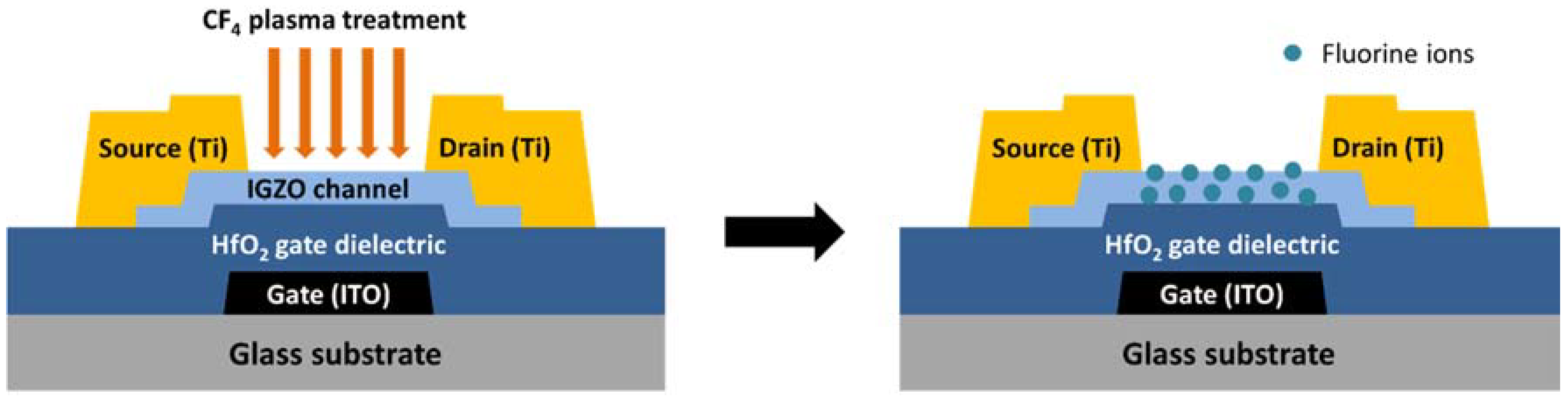
2. Device Fabrication

Figure 1 shows the schematic cross-sectional diagrams of the bottom-gate, top-contact a-IGZO TFTs. First, ITO film was patterned using photolithography and wet etching to form the gate electrode. The 180-nm thick HfO2 was then deposited as the gate insulator layer by RF sputtering in the mixed gas O2/Ar = 33% and annealed at 250 °C for 60 min. After patterning the contact hole, a 30 nm a-IGZO thin-film was deposited by RF sputtering in an Ar environment at room temperature. The active layer was then patterned by wet etching. A 160 nm Ti layer was deposited by thermal evaporation and using lift-off process to form source and drain (S/D) electrodes. Finally, a CF4 plasma treatment was carried out at the RF power of 15 W for 20 s, followed by a post-anneal at 250 °C for 60 min. Note that the low power and short treatment time of the plasma treatment ensured that the plasma treatment mainly acted on the IGZO active layer without serious damage.
The electrical characteristics and the bias stress voltage were examined using an Agilent 4145B semiconductor parameter analyzer in the dark. The transfer curves were measured at a source-to-drain voltage (VDS) of 5 V and the Vth was extracted from linear extrapolations of the square root plot of the drain current (IDS). The channel width (W) and length (L) of the a-IGZO TFT were 50 µm and 5 µm, respectively. The a-IGZO TFT without the passivation layer was used in the positive-gate bias stress (PGBS) to examine the ambient effect. The PGBS was carried out at the gate electrode (VGS = 6 V) with the source and drain electrodes grounded.

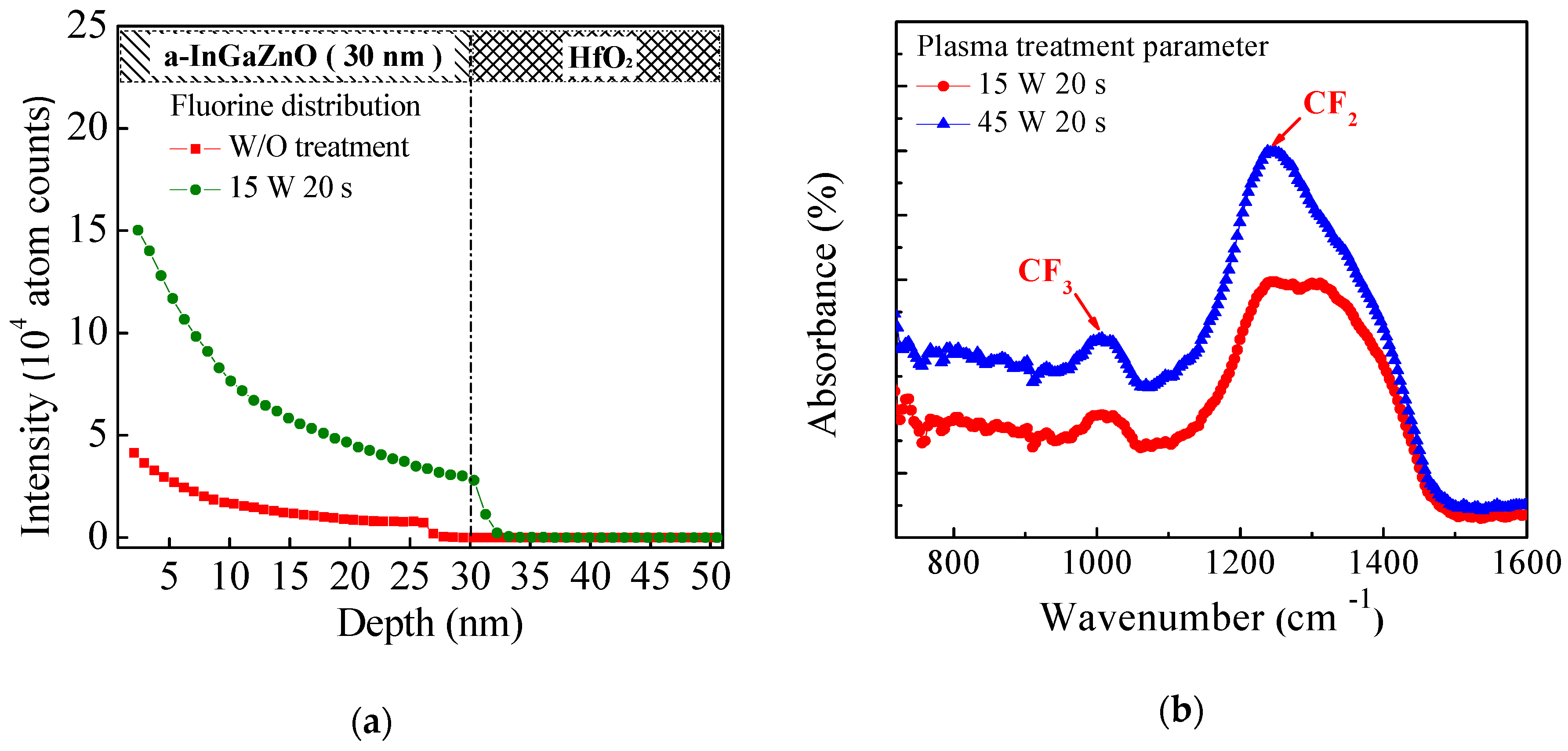
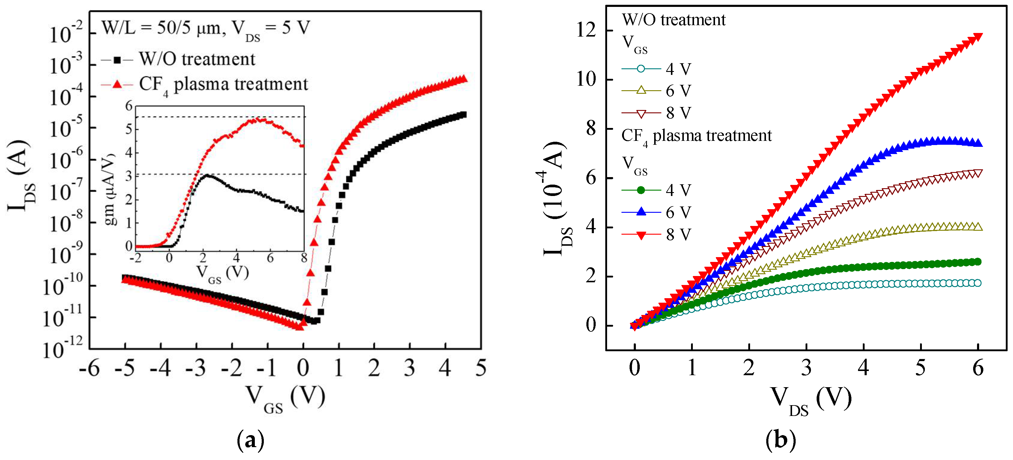
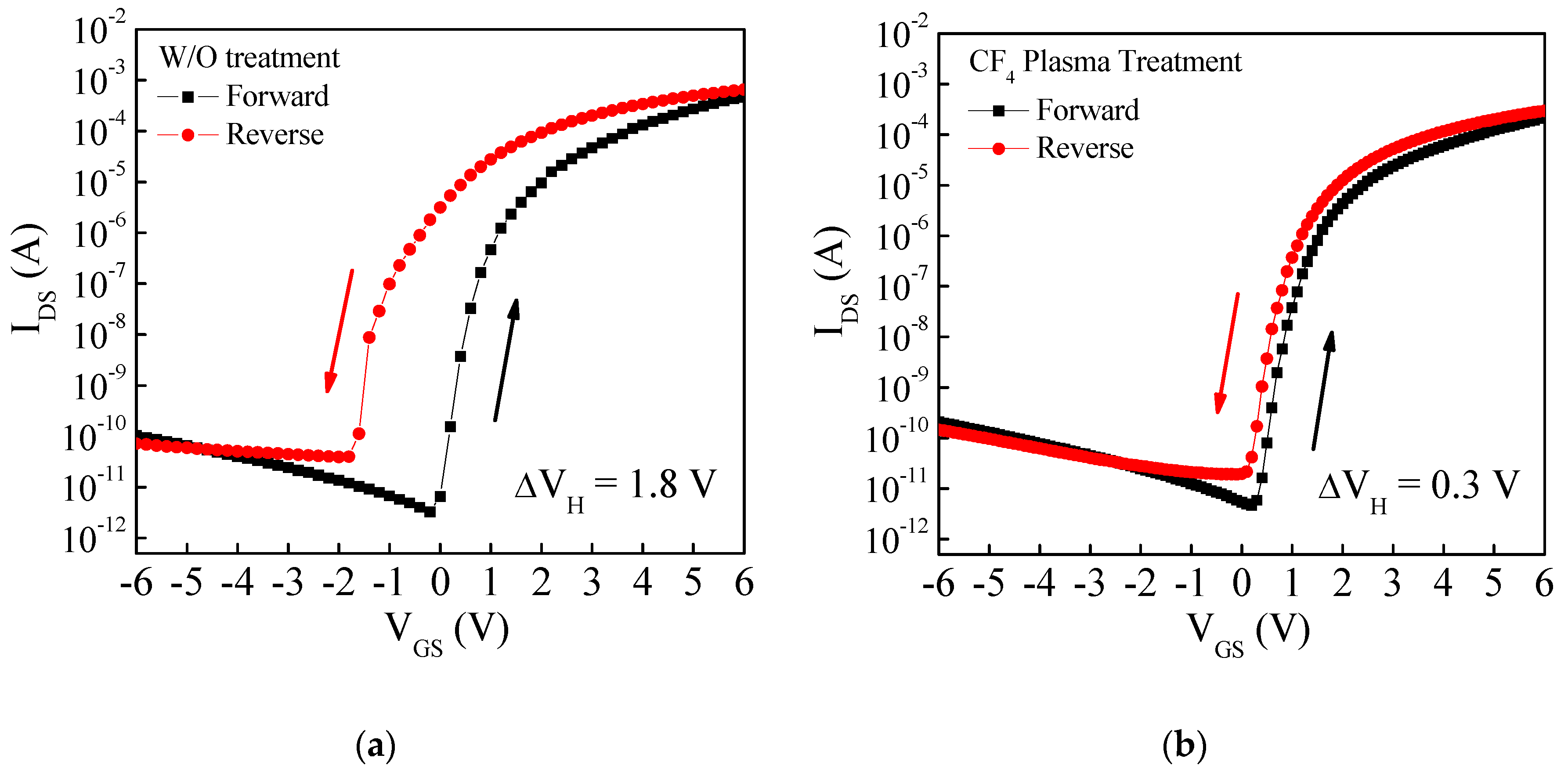
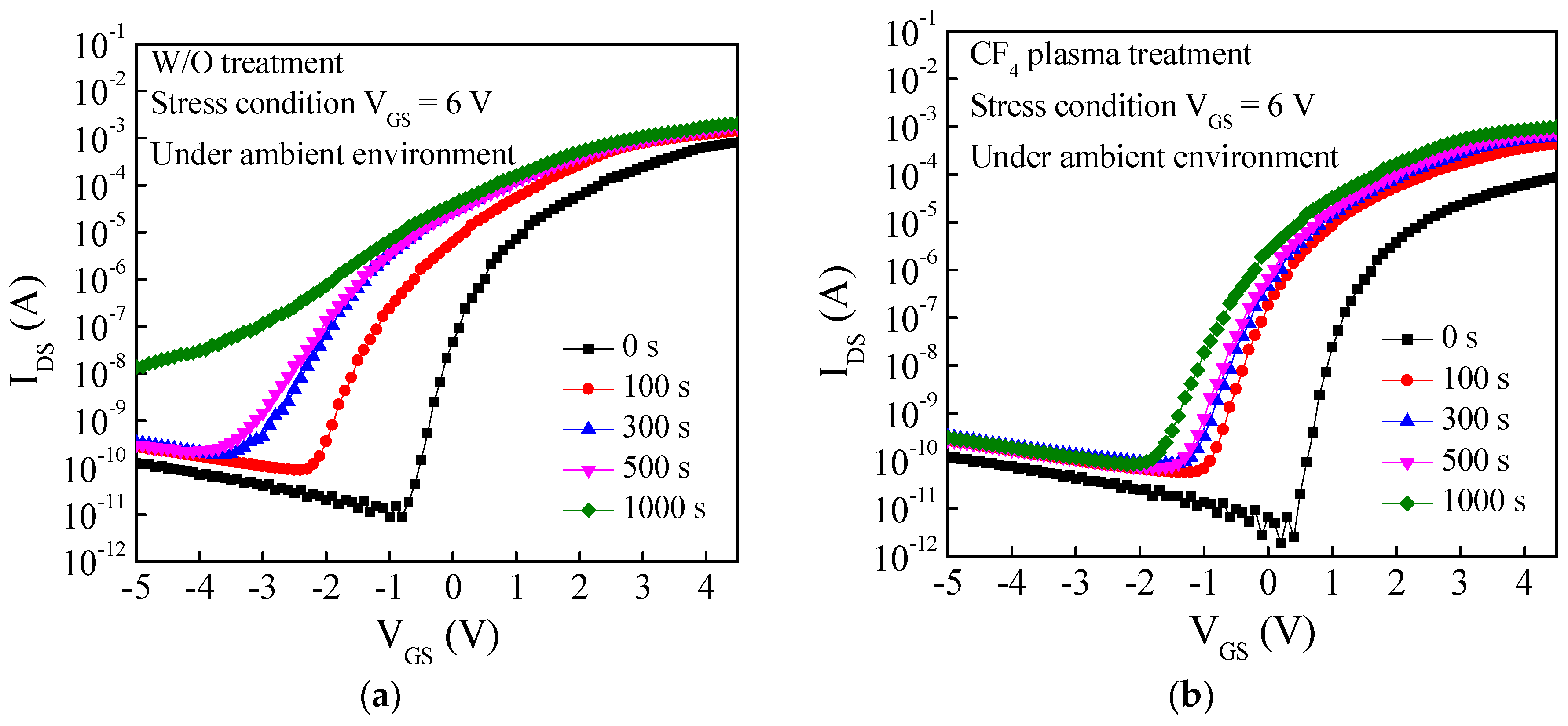
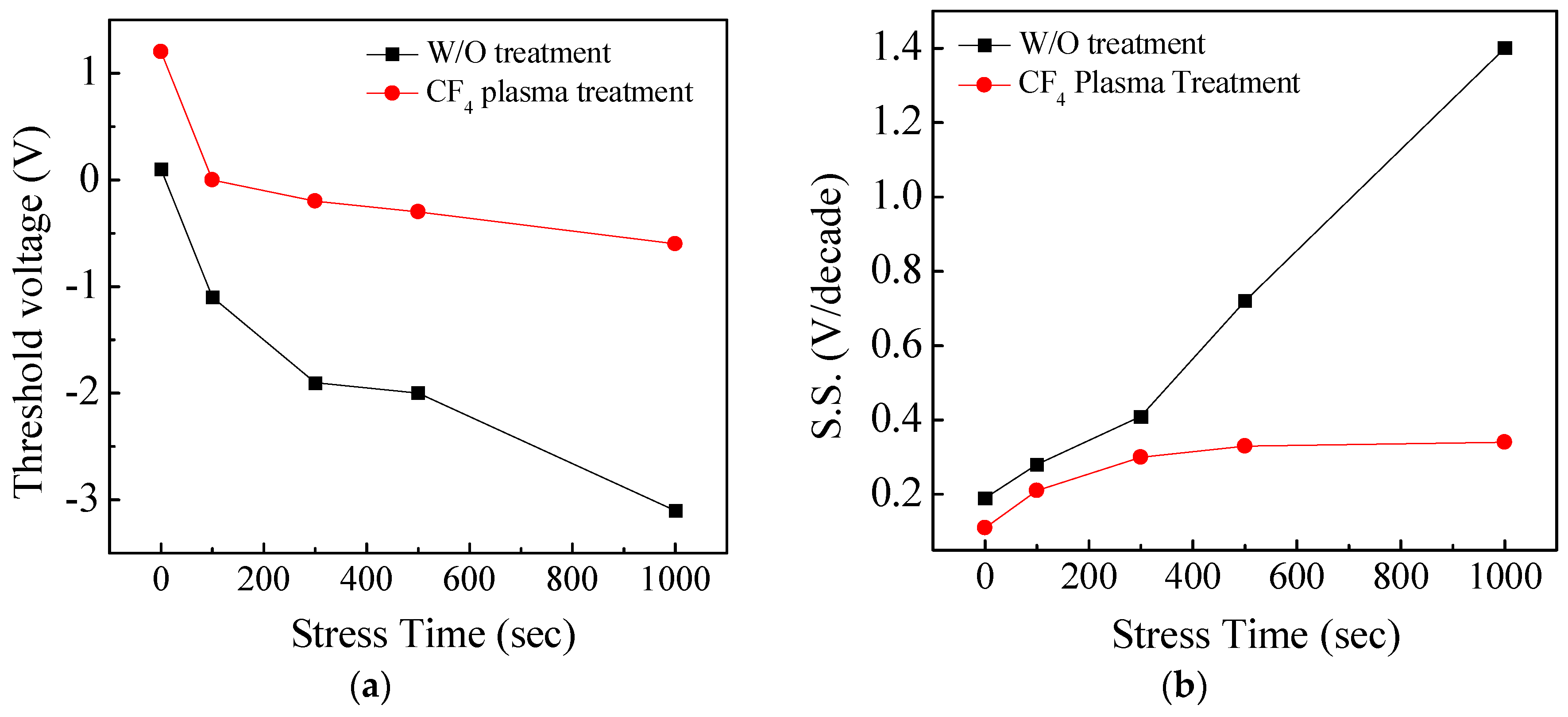
3. Results and Discussion

Figure 2a shows the secondary ion mass spectrometry (SIMS) depth profile in the stack of IGZO/HfO2/Si thin films. Compared with the untreated sample, the higher F concentration is observed in the sample with the CF4 plasma treatment, which indicates that the F atoms were successfully introduced into the IGZO film by the CF4 plasma treatment. In addition, the F atoms diffused towards the bulk of the IGZO film, and piled up at the IGZO/HfO2 interface. Figure 2b shows the fourier-transform infrared spectroscopy (FTIR) measurement of the IGZO film. The wave numbers of 980 cm−1 and 1240 cm−1 refer to the CF3 bond and CF2 bond, respectively [29]. Evidently, the IGZO film with 45 W treatment power has the higher CF2 peak, which indicates the more serious etching effect during the plasma treatment. CF4 is well-known as one of the reactive etching gas used in dry etching process. As the RF power increased, CF4 begins to dissociate into smaller components, such as CF2, CF3 and F radicals, which etch the underlying IGZO thin film. A small treatment power can reduce plasma damage in the IGZO active layer.
Figure 3a shows the transfer curves of the a-IGZO TFT with and without the CF4 plasma treatment. The linear mobility (µlinear), maximum transconductance (gmmax), threshold voltage (Vth), subthreshold swing (S.S.) and the on/off current ratio (Ion/Ioff) are summarized in Table 1. The µlinear is calculated from the gmmax measured at the VDS = 0.1 V using the linear-region drain current function, which is shown in the inset of Figure 3a. It is obvious that the a-IGZO TFT with the CF4 plasma treatment has a higher gmmax compared to the TFT without treatment, and that the linear mobility of the device is significantly improved from 30.2 cm2/V∙s (without treatment) to 54.6 cm2/V∙s (with CF4 plasma treatment). Moreover, the Vth and S.S. were slightly decreased from 1.50 V to 1.05 V, and 0.17 V/decade to 0.14 V/decade, respectively. The carrier mobility of TFT mainly depended on the carrier scattering or trapping in the channel layer. It is reasonable to suggest that the carrier concentration and trap density will dominate the carrier mobility. It is important to consider that the role of F atom in the IGZO film can not only passivate the defects by replacing the weakly bonded oxygen atoms or by directly filling the oxygen vacancy, but will also donate extra electrons due to the difference in electrovalence between the oxygen ion (O2−) and the fluorine ion (F) [28]. A lower interface trap density results in less carrier scattering, and the gate bias voltage can effectively induce more carrier concentration to transport in the IGZO channel due to the decreased trap density and the donated extra electrons. As a result, the carrier mobility of the a-IGZO TFT is improved by the CF4 plasma treatment. Figure 3b shows the output curves of the two a-IGZO TFTs measured at VGS = 4 V, 6 V, and 8 V. Both the TFTs exhibit n-type enhancement mode, and the IDS saturated at the high VDS region. Compared with the untreated device, the higher IDS observed in the a-IGZO TFT with the CF4 plasma treatment resulted from the increased carrier mobility. The on currents measured at VDS = 6 V and VGS = 8 V of the plasma treatment TFT and the untreated TFT are 1180 µA and 623 µA, respectively. As a result, the electrical performance of the a-IGZO TFT can be significantly improved by the CF4 plasma treatment.
Figure 4 shows the hysteresis measurement of the a-IGZO TFT with and without the CF4 plasma treatment. It can be observed that the hysteresis voltage (∆VH) abnormally shifted towards the negative direction and the a-IGZO TFT with the plasma treatment has a smaller ∆VH. The ∆VH of the a-IGZO TFT with and without the CF4 plasma treatment are −1.8 V and −0.3 V, respectively. The negative Vth shift is due to the carrier creation in the IGZO film, which is mainly from the enhanced control and from using the high-k HfO2 as the gate insulator. When the gate bias is applied to the TFT, the HfO2 gate insulator will provide a strong electric field near the IGZO/HfO2 interface to bend the Fermi level in the deep of the band gap. The energy level of the neutral oxygen vacancies (VO), which is higher than the Fermi level, will be ionized (VO++) and two electrons will be contributed to the IGZO film because the highest electron energy level in the IGZO band gap cannot reach the energy level of VO [10,18]. Therefore, the extra free electrons generated during the forward sweep of the gate bias will cause the negative Vth shift in the reverse sweep of the gate bias.
Figure 5a,b shows the transfer curves of the a-IGZO TFT with and without the CF4 plasma treatment under the PGBS (VGS = 6 V). The TFTs were fabricated without the passivation layer to examine the ambient effect. For the a-IGZO TFT without treatment, the device suffers from a more serious negative Vth shift and a S.S. degradation, as shown in Figure 6a,b, which are mainly due to the moisture from the ambient atmosphere absorbed onto the IGZO surface. The absorbed moisture will bond to the metal element in IGZO to form metal-hydroxide (M-OH) bonds, which act as donor-like states to provide extra electrons, but also increase the density of state within the IGZO film [18]. Thus, the absorbed moisture will cause a negative Vth shift and an S.S. degradation. For the a-IGZO TFT with the CF4 plasma treatment, the oxygen vacancies or the weak oxygen bonds on the IGZO surface are replaced by the F ions, as shown in Figure 2b. The M-F bonds are stronger and more stable than the M-O bond, and thus the formation of the M-OH bonds is suppressed by the incorporation of F. In summary, the a-IGZO TFT with HfO2 as the gate insulator and the CF4 plasma treatment not only acquires a higher immunity against humidity from ambient atmosphere, but also significantly improves the device performance.

4. Conclusions

We have demonstrated that the CF4 plasma treatment can significantly improve the electrical performance and reliability of the a-IGZO TFT with a HfO2 gate insulator. After the plasma treatment at 15 W for 20 s on the IGZO active layer, the carrier mobility significantly improved from 30.2 cm2/V∙s to 54.6 cm2/V∙s. This can be attributed to the incorporated F providing additional electrons in the IGZO, and in parallel passivating the interface traps at the IGZO/HfO2 interface. Low interface traps result in less carrier scattering, which results in an increased carrier mobility. Moreover, it was found that the CF4 plasma treatment can effectively suppress the hysteresis effect and enhance the device’s immunity against humidity from the ambient atmosphere. It is believed that the CF4 plasma treatment can improve the electrical performance and reliability of the a-IGZO TFT with a HfO2 gate insulator.

Author Contributions

Conceptualization, C.-L.F. and F.-P.T.; Formal Analysis, F.-P.T. and C.-Y.T.; Investigation, F.-P.T. and C.-Y.T.; Resources, C.-L.F.; Writing-Original Draft Preparation, F.-P.T. and C.-Y.T.; Writing-Review & Editing, C.-L.F.; Supervision, C.-L.F.

Funding

This research was funded by the National Science Council of Taiwan under contract grant number NSC 106-2622-E-011-015-CC3.

Acknowledgments

The authors would like to acknowledge the financial support of the National Science Council of Taiwan under contract no. NSC 106-2622-E-011-015-CC3 and the Taiwan Building Technology Center (TBTC) of National Taiwan University of Science and Technology (NTUST).

Conflicts of Interest

The authors declare no conflict of interest.

References

  1. Nomura, K.; Ohta, H.; Takagi, A.; Kamiya, T.; Hirano, M.; Hosono, H. Room-temperature fabrication of transparent flexible thin-film transistors using amorphous oxide semiconductors. Nature 2004, 432, 488–492. [Google Scholar] [CrossRef] [PubMed]
  2. Yabuta, H.; Sano, M.; Abe, K.; Aiba, T.; Den, T.; Kumomi, H.; Nomura, K.; Kamiya, T.; Hosono, H. High-mobility thin-film transistor with amorphous InGaZnO4 channel fabricated by room temperature rf-magetron sputtering. Appl. Phys. Lett. 2006, 89, 112123. [Google Scholar] [CrossRef]
  3. Suresh, A.; Wellenius, P.; Dhawan, A.; Muth, J. Room temperature pulsed laser deposited indium gallium zinc oxide channel based transparent thin film transistors. Appl. Phys. Lett. 2007, 90, 123512. [Google Scholar] [CrossRef]
  4. Kamiya, T.; Nomura, K.; Hosono, H. Origins of High Mobility and Low Operation Voltage of Amorphous Oxide TFTs: Electronic Structure, Electron Transport, Defects and Doping. J. Disp. Technol. 2009, 5, 273–288. [Google Scholar] [CrossRef]
  5. Mativenga, M.; Choi, M.H.; Choi, J.W.; Jang, J. Transparent Flexible Circuits Based on Amorphous-Indium-gallium-Zinc-Oxide Thin-Film Transistors. IEEE Electron Device Lett. 2011, 32, 170–172. [Google Scholar] [CrossRef]
  6. Lee, I.; Lee, S.; Gu, J.; Kim, K.; Cho, W. Comparative Study of Device Performance and Reliability in Amorphous InGaZnO Thin-Film Transistors with Various High-k Gate Dielectrics. Jpn. J. Appl. Phys. 2013, 52, 06GE05. [Google Scholar] [CrossRef]
  7. Hsu, H.; Chang, C.; Cheng, C.; Chen, P.; Chiu, Y.; Chiou, P.; Cheng, C. High Mobility Field-Effect Thin Film Transistor Using Room-Temperature High-k Gate Dielectrics. J. Disp. Technol. 2014, 10, 875–881. [Google Scholar] [CrossRef]
  8. Pan, T.; Chen, C.; Liu, J.; Her, J.; Koyama, K. Electrical and Reliability Characteristics of High-k HoTiO3 a-InGaZnO Thin-Film Transistors. IEEE Electron Device Lett. 2014, 35, 66–68. [Google Scholar] [CrossRef]
  9. Shao, Y.; Xiao, X.; He, X.; Deng, W.; Zhang, S. Low-Voltage a-InGaZnO Thin-Film Transistors With Anodized Thin HfO2 Gate Dielectric. IEEE Electron Device Lett. 2015, 36, 573–575. [Google Scholar] [CrossRef]
  10. Huang, X.D.; Song, J.Q.; Lai, P.T. Positive Gate Bias and Temperature-Induced Instability of a-InGaZnO Thin-Film Transistor with ZrLaO Gate Dielectric. IEEE Trans. Electron Devices 2016, 63, 1899–1903. [Google Scholar] [CrossRef]
  11. Park, J.C.; Cho, I.; Cho, E.; Kim, D.H.; Jeong, C.; Kwon, H. Comparative Study of ZrO2 and HfO2 as a High-k Dielectric for Amorphous InGaZnO Thin Film Transistors. J. Nanoelectron. Optoelectron. 2014, 9, 67–70. [Google Scholar] [CrossRef]
  12. Kim, H.; Mclntyre, P.C.; Saraswat, K.C. Effects of crystallization on the electrical properties of ultrathin HfO2 dielectrics grown by atomic layer deposition. Appl. Phys. Lett. 2003, 82, 106–108. [Google Scholar] [CrossRef]
  13. Hu, H.; Zhu, C.; Lu, Y.F.; Wu, Y.H.; Liew, T.; Li, M.F.; Cho, B.J.; Choi, W.K.; Yakovlev, N. Physical and electrical characterization of HfO2 metal-insulator-metal capacitors for Si analog circuit applications. J. Appl. Phys. 2003, 94, 551–557. [Google Scholar] [CrossRef]
  14. Lin, Y.; Chou, J. Temperature Effects on a-IGZO Thin Film Transistors Using HfO2 Gate Dielectric Material. J. Nanomater. 2014, 2014, 72. [Google Scholar] [CrossRef]
  15. Son, D.; Kim, D.; Sung, S.; Jung, E.; Kang, J. High performance and the low voltage operating InGaZnO thin film transistor. Curr. Appl. Phys. 2010, 10, e157–e160. [Google Scholar] [CrossRef]
  16. Chun, Y.S.; Chang, S.; Lee, S.Y. Effects of gate insulators on the performance of a-IGZO TFT fabricated at room-temperature. Micoelectron. Eng. 2011, 88, 1590–1593. [Google Scholar] [CrossRef]
  17. Na, J.H.; Kitamura, M.; Arakawa, Y. High field-effect mobility amorphous InGaZnO transistors with aluminum electrodes. Appl. Phys. Lett. 2008, 93, 063501. [Google Scholar] [CrossRef]
  18. Choi, S.; Kim, H.; Jo, C.; Kim, H.; Choi, S.; Kim, D.M.; Park, J.; Kim, D.H. A Study on the Degradation of In-Ga-Zn-O Thin-Film Transistors under Current Stress by Local Variations in Density of States and Trapped Charge Distribution. IEEE Electron Device Lett. 2015, 36, 690–692. [Google Scholar] [CrossRef]
  19. Lee, J.; Cho, I.; Lee, J.; Kwon, H. Bias-stress-induced stretched-exponential time dependence of threshold voltage shift in InGaZnO thin film transistors. Appl. Phys. Lett. 2008, 93, 093504. [Google Scholar] [CrossRef]
  20. Huang, X.D.; Song, J.Q.; Lai, P.T. Improved Stability of a-InGaZnO Thin-Film Transistor under Positive Gate Bias Stress by Using Fluorine Plasma Treatment. IEEE Electron Device Lett. 2017, 38, 576–579. [Google Scholar] [CrossRef]
  21. Liu, X.; Wang, L.L.; Hu, H.; Lu, X.; Wang, K.; Wang, G.; Zhang, S. Performance and Stability Improvements of Back-Channel-Etched Amorphous Indium-Gallium-Zinc Thin-Film Transistors by CF4+O2 Plasma Treatment. IEEE Electron Device Lett. 2015, 36, 911–913. [Google Scholar] [CrossRef]
  22. Qian, L.Z.; Lai, P.T. Fluorinated InGaZnO Thin-Film Transistor with HfLaO Gate Dielectric. IEEE Electron Device Lett. 2014, 35, 363–365. [Google Scholar] [CrossRef]
  23. Jiang, J.; Toda, T.; Hing, M.P.; Wang, D.; Furuta, M. Highly stable fluorine-passivated In-Ga-Zn-O thin-film transistors under positive gate bias and temperature stress. Appl. Phys. Express 2014, 7, 114103. [Google Scholar] [CrossRef]
  24. Yamazaki, H.; Ishikawa, Y.; Fujii, M.; Ueoka, Y.; Fujiwara, M.; Takahashi, E.; Andoh, Y.; Maejima, N.; Matsui, H.; Matsui, F.; et al. The Influence of Fluorinated Silicon Nitride Gate Insulator on Positive Bias Stability toward Highly Reliability Amorphous InGaZnO Thin-Film Transistors. ECS J. Solid State Sci. Technol. 2014, 3, Q20–Q23. [Google Scholar] [CrossRef]
  25. Jiang, J.; Furuta, M.; Wang, D. Self-Aligned Bottom-Gate In-Ga-Zn-O Thin-Film Transistor with Source/Drain Regions Formed by Direct Deposition of Fluorinated Silicon Nitride. IEEE Electron Device Lett. 2014, 35, 933–935. [Google Scholar] [CrossRef]
  26. Furuta, M.; Jiang, J.; Hung, M.P.; Toda, T.; Wang, D.; Tatsuoka, G. Suppression of Negative Gate Bias and Illumination Stress Degradation by Fluorine-Passivated In-Ga-Zn-O Thin-Film Transistors. ECS J. Solid State Sci. Technol. 2016, 5, Q88–Q91. [Google Scholar] [CrossRef]
  27. Um, J.K.; Lee, S.; Jin, S.; Mativenga, M.; Oh, S.Y.; Lee, C.H.; Jang, J. High-Performance Homojunction a-IGZO TFTs with Selectively Defined Low-Resistive a-IGZO Source/Drain Electrodes. IEEE Trans. Electron Devices 2015, 62, 2212–2217. [Google Scholar] [CrossRef]
  28. Seo, J.; Jeon, J.; Hwang, Y.H.; Park, H.; Ryu, M.; Park, S.K.; Bae, B. Solution-Processed Flexible Fluorine-doped Indium Zinc Oxide Thin-Film Transistors Fabricated on Plastic Film at Low Temperature. Sci. Rep. 2013, 3, 2085. [Google Scholar] [CrossRef] [PubMed]
  29. Banuerfeldt, G.F.; Arbilla, G. Kinetic Analysis of the Chenical Processes in the Decomposition of Gaseous Dielectrics by a Non-Equilibrium Plasma-Part1:CF4 and CF4/O2. J. Braz. Chem. Soc. 2000, 11, 121–128. [Google Scholar] [CrossRef]
Figure 1. Schematic cross-sectional diagrams of a-IGZO TFT with CF4 plasma treatment.
Materials 11 00824 g001
Figure 2. (a) SIMS depth profiles; (b) FTIR measurement for the untreated sample and the sample with the CF4 plasma treatment after annealing at 250 °C for 60 min.
Materials 11 00824 g002
Figure 3. (a) Transfer curves (IDS-VGS); (b) Output curves (IDS-VDS) of the a-IGZO TFT without treatment and with a 15 W, 20 s CF4 plasma treatment. Inset of Figure 3a shows the transconductance measured at VDS = 0.1 V.
Materials 11 00824 g003
Figure 4. Hysteresis measurement of amorphous indium-gallium-zinc oxide (a-IGZO) thin-film transistor (TFT) with and without the CF4 plasma treatment.
Materials 11 00824 g004
Figure 5. Transfer curves (IDS-VGS) of a-IGZO TFT with and without the CF4 plasma treatment under positive gate bias stress (PGBS) (VGS = 6 V).
Materials 11 00824 g005
Figure 6. (a) Vth; (b) S.S. as function of PGBS time of a-IGZO TFT.
Materials 11 00824 g006
Table 1. Effects of the CF4 plasma treatment on electrical performance parameters of the fabricated a-IGZO TFTs with HfO2 gate dielectric.
Electrical ParametersWithout TreatmentWith CF4 Plasma Treatment
µlinear (cm2/V∙s)30.254.6
gmmax (A/V)3.02 × 10−65.46 × 10−6
Vth (V)1.501.05
S.S. (V/decade)0.170.14
Ion/Ioff3.5 × 1067.44 × 107

