Properties of Novel Non-Silicon Materials for Photovoltaic Applications: A First-Principle Insight
by
 ,
,
Murugesan Rasukkannu
1,* ,
,
Dhayalan Velauthapillai
1,
Federico Bianchini
2 and
Ponniah Vajeeston
2 1
Department of Computing, Mathematics and Physics, Western Norway University of Applied Sciences, Inndalsveien 28, 5063 Bergen, Norway
2
Department of Chemistry, Center for Materials Science and Nanotechnology, University of Oslo, Box 1033, Blindern, N-0315 Oslo, Norway
*
Author to whom correspondence should be addressed.
Materials 2018, 11(10), 2006; https://doi.org/10.3390/ma11102006
Submission received: 18 September 2018
/
Revised: 1 October 2018
/
Accepted: 11 October 2018
/
Published: 17 October 2018
(This article belongs to the Special Issue Density Functional Theory (DFT) Calculation of Materials Properties)
Abstract
:Due to the low absorption coefficients of crystalline silicon-based solar cells, researchers have focused on non-silicon semiconductors with direct band gaps for the development of novel photovoltaic devices. In this study, we use density functional theory to model the electronic structure of a large database of candidates to identify materials with ideal properties for photovoltaic applications. The first screening is operated at the GGA level to select only materials with a sufficiently small direct band gap. We extracted twenty-seven candidates from an initial population of thousands, exhibiting GGA band gap in the range 0.5–1 eV. More accurate calculations using a hybrid functional were performed on this subset. Based on this, we present a detailed first-principle investigation of the four optimal compounds, namely, TlBiS2, Ba3BiN, Ag2BaS2, and ZrSO. The direct band gap of these materials is between 1.1 and 2.26 eV. In the visible region, the absorption peaks that appear in the optical spectra for these compounds indicate high absorption intensity. Furthermore, we have investigated the structural and mechanical stability of these compounds and calculated electron effective masses. Based on in-depth analysis, we have identified TlBiS2, Ba3BiN, Ag2BaS2, and ZrSO as very promising candidates for photovoltaic applications.
1. Introduction
The solar energy reaching the earth amounts to approximately ten thousand times the primary energy usage by the world population. Solar photovoltaic cells are among the most important technologies for clean energy production. It is predicted that in future, the power from solar photovoltaic modules will reach the terawatt level [1]. Photovoltaic (PV) technology is currently dominated by silicon solar cells. If we look at the worldwide scenario, more than 80% of the installed PV modules are mainly mono or multi-crystalline silicon based [1]. However, researchers are making considerable efforts to develop solar cells based on alternative materials because silicon is an indirect band gap material with a low absorption coefficient. Novel materials considered for PV applications include copper zinc tin sulfide (CZTS), ternary, binary, and multinary compounds with a direct band gap, enabling high absorption properties. High photon conversion efficiency and low production cost are the other desired features of these alternative materials. There is also considerable interest in the research community to find ways to develop solar cells that have efficiencies greater than the Shockley-Queisser limit of 32% [2].
The development of non-silicon materials is a very active field, and several significant signs of progress have been made recently [1]. In the future, non-silicon materials will most likely be produced using thin film technologies, with a resulting device thickness in the order of 2 μm. Despite the crucial role played by these compounds for the next generation of energy materials, the current knowledge of the optical and electronic properties of these compounds is inadequate. Non-silicon materials such as organic semiconductors may become the main candidates for future photovoltaic devices, even though they have low stability [3]. To be a promising solar cell material, a semiconductor preferably have a direct band gap with an appropriate band gap value resulting in efficient absorption of the solar spectrum.
Furthermore, it can be used in a junction formation, which is appropriate for guiding the electrical processes involved in energy conversion [4]. A variety of basic materials, GaAs, InP, CdTe, CuInSe2 to name a few, and large band gap materials such as ZnO, CdS, ZnCdS used as window layers in creating heterojunctions have been studied extensively [4]. Reducing production cost is one of the priorities in selecting materials for PV technologies. Compared to mono-crystalline Silicon solar cells, the production cost for poly-crystalline Silicon solar cells is lower, but the efficiency is lower [5]. According to Mitchell [6], materials that require only a few micrometers of thickness to absorb the solar spectrum and photo-carriers effectively are created close to the electrical junction. One way to minimize material usage is to choose direct band gap materials over indirect band gap materials, since direct band gap solar cells could be made substantially thinner [7]. Due to the low absorption, polycrystalline silicon solar cell structures must have a thickness in the range of 200 μm, which makes the overall cost higher. We have earlier reported several non-silicon intermediate band gap materials that can be used for solar cell applications [8,9]. Our main aim in this study is to propose non-silicon based direct band gap materials with highly efficient photoelectric properties such that material costs become lower.
As one of the most effective and accurate computational methods for modelling atomistic systems, density functional theory (DFT) has been widely applied in this work to extensively analyze the electronic band structure of thousand non-silicon based materials in order to identify candidates that have a band gap between 0.5 eV and 1.1 eV. The band structure calculation for these presented materials is based on the generalized gradient approximation (GGA) that underestimates the value of the band gap. However, this technique is efficient and time-effective in terms of computational resources, and it can be used for an initial screening of a large number of compounds. The initial structural parameters of thousand compounds were directly taken from the ICSD database [10], and then the GGA band gap for thousands of non-silicon compounds were calculated in our DFTB database [11]. These are multinary compounds including conductors, semiconductors, and insulators. Among these thousand non-silicon compounds, we considered twenty-seven of them with GGA band gap values in the range of 0.5–1.1 eV (Table S1 of Supplementary Materials). Among these twenty-seven compounds, we identified fourteen compounds as direct band gap semiconductors and thirteen as indirect band gap semiconductors. We carried out a study on both the electronic and optical properties of twenty-seven semiconductors (both direct and indirect). Our study of the optical properties of semiconductor materials showed that four direct band gaps among the twenty-seven materials had higher absorption coefficients in the visible region. Due to the space constraint, the optical properties of all the twenty-seven semiconductors are not presented in the supporting information.
We carry out a comprehensive study on these four materials, namely TlBiS2, Ba3BiN, Ag2BaS2, and ZrSO, and report accurate electronic structure results for these four compounds by employing a more accurate calculation based on the screened–exchange hybrid density functional Heyd-Scuseria-Ernzerhof (HSE06). HSE06 helps to identify the contributions of individual elements to the electronic structure of the compounds. We also study the structural and mechanical stability and the optical properties of these four materials to verify the applicability of these four materials for photovoltaic applications. In a recently published article, we focused on TlBiS2, and have presented electronic band structure and optical spectra based on spin-orbit coupling (SOC) [12].
2. Computational Details
We employed DFT analysis using Vienna ab initio simulation package (VASP, 5.4.1. Feb. 16) with the projected augmented plane-wave (PAW) approach [13] to study the electronic structures of TlBiS2, Ba3BiN, Ag2BaS2, and ZrSO. The Perdew–Burke–Ernzerhof (PBE) functional is used to treat exchange and correlation within the GGA approach [14]. To obtain an improved description of the interaction between oxygen and the transition metal atoms, we used the Hubbard parameter correction (DFT+U), following the rotationally invariant form [15,16,17]. The full details about the computed U and J values are presented in the DFTBD database website [11]. These DFT+U calculations are used for the structural optimisation of the considered compounds, as the relaxation using HSE06 is time-consuming and has no significant effect on the structural properties. Ground-state geometries are calculated using the conjugate-gradient algorithm with a force convergence threshold of 10−3 eV Å−1, and minimizing the stress tensor and the Hellman-Feynman forces. In order to achieve better and detailed band structures, we used the hybrid functional of Heyd–Scuseria–Ernzerhof (HSE06). For the standard HSE06 functional, the screened parameter was assigned to 0.2 A−1, and the screened Hartree-Fock (HF) exchange was set to 30% mixing with the PBE exchange functional [18]. The cut-off energy for the plane-wave basis expansion was set to 600 eV, and for Brillouin zone integration we used a 6 × 6 × 6 Г-centered Monkhorst-pack k-point mesh. In both calculations (i.e., PBE and HSE06), this setting is used.
Solving the Casida’s equation is one of the best approaches for determining the dielectric function [19]. We have summed the contributions over a number of 8 × 8 × 8 k-points grids, shifted with respect to each other to reproduce16 × 16 × 16 Г-centered k-points mesh, using a plane-wave cut-off of 410 eV for both GW and Bethe-Salpeter equation (BSE). To get a more accurate peak position and intensities in optical spectra, the optical calculation counts the contribution from 200 electronic bands. For all of these computations, the initial structural parameters were taken directly from the ICSD database [10]. The information about the high symmetric points of the k-vector in the Brillouin zone was taken from the Bilbao Crystallographic Server [20,21,22].
A frozen phonon calculation was performed on suitable supercells of the relaxed structures, generated using the phonopy program (1.9.2). This software is also used to obtain the phonon dispersion curve and the phonon density of states from the converged calculations [23,24]. The atomic displacement of 0.0075 is used, with symmetry considerations to obtain the force constants for the phonon calculations. The displacements in opposite directions along all the axes were incorporated into the calculations to improve the precision. The force calculations were performed using the VASP code (DFT+U level), and the resulting data were imported into PHONOPY. The dynamical matrices were derived from the force constants, and phonon DOS curves were computed using the Monkhorst-Pack scheme [25].
3. Results and Discussion
3.1. Structural Properties
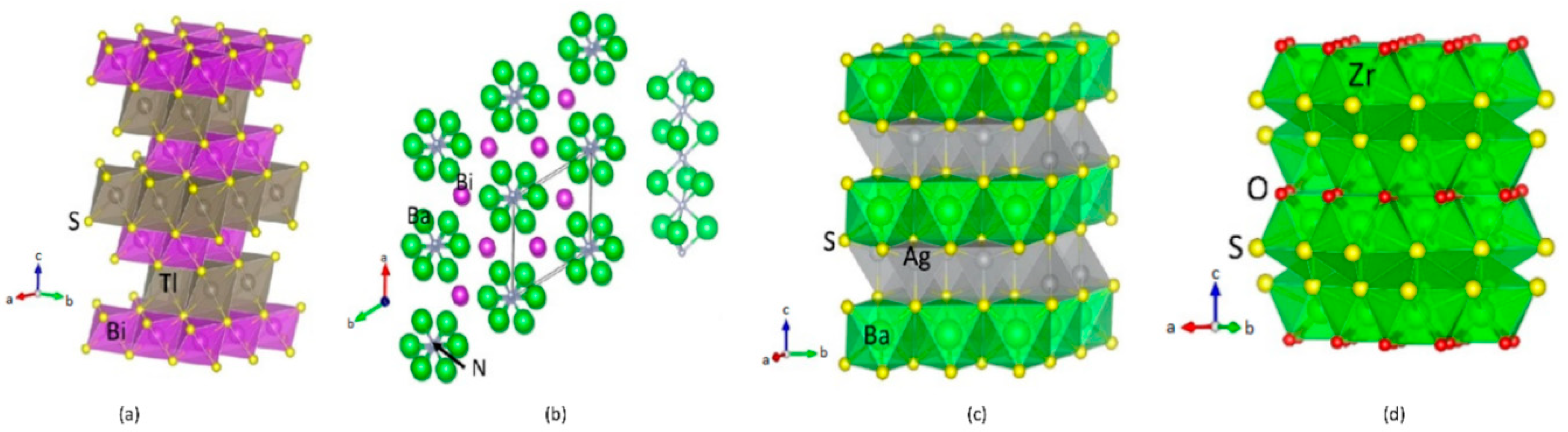
TlBiS2: TlBiS2 has rhombohedral structures with space group D5 3d (R-3m, Space group No. 166), similar to Bi2Te3. There are four atoms, namely, 1-Tl, 1-Bi, and 2-S positioned in layers normal to the three-fold axis in the arrangement Tl-S-Bi-S, as shown in Figure 1a. Each Tl/Bi layer is placed between two S layers, which indicates a strong interlayer coupling so that the crystal structure is substantially three-dimensional. Tl, Bi, and S are placed at the (0, 0, 0), (0.5, 0.5, 0.5), and (±u, ±u, ±u) sites, respectively. This structure has inversion symmetry where both Bi and Tl represent inversion centers. The basic TlBiS2 structure is a simple NaCl-type lattice. It is similar to ABQ2-type compounds (A, B and Q are monovalent atom, trivalent atom and chalcogen respectively). The TlBiS2 structure is rhombohedral along the cubic [111] direction and matching to the c axis of the primitive hexagonal arrangement. The sum of the ionic radii for a coordination number (CN) of 6 is 2.87 Å for Bi3+/S2− and 3.34 Å for Tl+/S2− [26]. The experimentally-determined and theoretically-derived bond length matches well for Bi-S, but for the Tl-S distance the value is about 5.3% smaller. Our calculated lattice parameters and the positional parameters all fitted well with the experimental findings (see Table S2) [26].
Ba3BiN: (Ba3N)Bi crystallizes in a hexagonal anti-perovskite variant of the BaNiO3 structure type (P63/mmc, space group No. 194, Z = 2). This phase consists of Ba6N octahedral units sharing faces formed with three Ba ions according to a rod-like structure along [001] (see Figure 1b). The calculated Ba-N distance is 2.677 Å which compares well with those in sub-nitrides with nitrogen species in octahedral coordination [27,28]. Hexagonal perovskite crystal structures can only be expected for compounds containing alkaline-earth metal species with large radii. Hence, the resulting distance d (N-N) and the Coulomb repulsion between N3− in face-sharing octahedra has to be formed. The resulting distance N-N is 3.3218 Å is sufficiently large.
Ag2BaS2: Ag2BaS2 crystallises in the trigonal CaA12Si2-type structure, a = 4.386 (1) A, c = 7.194 (2) A, space group P3m1, Z = 1, where S and Ag atoms are arranged in the chemically ordered double-corrugated hexagonal layers and Ca atoms are intercalated between them [29], as shown in Figure 1c. These layers can, in turn, be described as being made up from two stacked AgS layers, with each layer being a two-dimensional infinite net of chair-like six-membered rings. Every atom in the Ag2S2 layer is four-coordinate, but the coordination environment is very different for Ag and S. Each Ag is surrounded by four S atoms, forming a distorted tetrahedron. The S is also four-coordinate in Ag, but the environment is most unusual, a flipped tetrahedron or umbrella shape.
ZrSO: ZrSO crystalizes in cubic (P213, space group No. 198) and tetragonal (P4/nmm, space group No. 129) form [30,31]. Tetragonal ZrSO crystallises in the PbFCl-type structure. The form of this phase has not yet been synthesized [31]. All preparations techniques proved that the tetragonal phase was always accompanied by considerable proportions of cubic ZrSO, and in some cases, even by ZrO2. It seemed likely, therefore, that the tetragonal phase also contains oxygen [31]. According to our theoretical energy volume curve (see Figure S1), the cubic form is more stable than the tetragonal form and the energy difference between these two structures is very small (36 meV/f.u.). Moreover, it is clear from Figure S1 that the energy minima for these two structures are well separated, and the energy well is deep enough to stabilize the individual phases. We can thus conclude that this phase can be experimentally stabilized using a high-pressure technique.
There are four S and three O atoms surround each Zr atom in the cubic phase. The S atoms form a stretched tetrahedron with one Zr-S separation of 2.61 Å and three of 2.63 Å. The O atoms form an equilateral triangle centered at the Zr site, in such a way that there is an O atom in each of the stretched faces of the S atoms tetrahedron. At a distance of 2.13 Å from each oxygen atom, the Zr atom is slightly out of the plane of the oxygen triangle. The configuration may be regarded as a distorted octahedron consisting of three S atoms and three O atoms, with an extra sulfur atom above the center of the face of the octahedron driven by the oxygen atoms. From this point of view, the co-ordination of zirconium is quite similar to that observed in K3ZrF7. The separations of S-S and S-O are 3.59 and 2.96 Å, respectively. These separations are shorter than the sum of the radii (3.68 Å for S-S and 3–24 Å for S-O) owing to the sharing of edges between the coordination polyhedra [30].
3.2. Electronic Properties
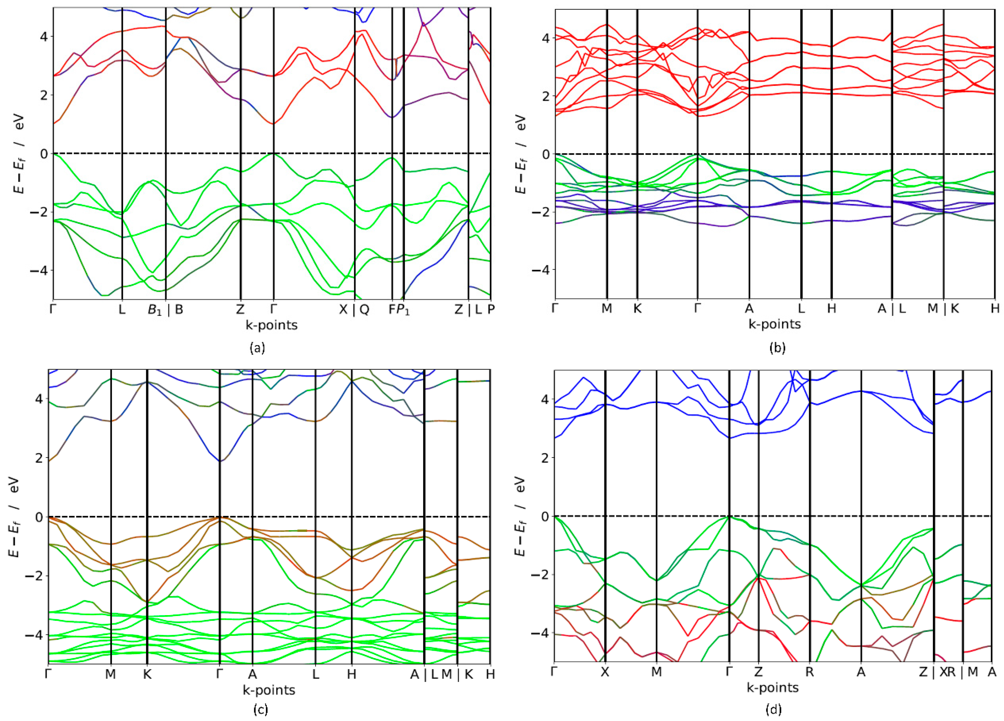
In order to investigate the potential applicability of non-silicon semiconductors as a light-harvesting medium, the band gap of these materials is a crucial factor that needs to be further explored. Both short-circuit current and open-circuit voltage is regulated by the band gap of the photoactive semiconductors. Broader band gap leads to higher open-circuit voltage but fewer excited electrons, which results in lower short-circuit current. Narrower band gap leads to low open circuit voltage but more excited electrons, which result in larger short-circuit current. The ideal solar cell is theoretically shown to have a maximum of 32% efficiency with an optimal band gap Eg = 1.4 eV is [2]. In real cells, the solar spectrum is a broad energy spectrum and it does not match the band gap well where thermalisation loss occurs, which eventually results in efficiencies below the detailed-balance limit [2]. Band gap calculation using electronic band structures gives a promising opportunity to identify suitable PV materials. The calculated band structure of trigonal-TlBiS2, hexagonal-Ba3BiN, trigonal-Ag2BaS2 and tetragonal-ZrSO crystals along a high-symmetry path in the first Brillouin zone are presented in Figure 2. For electronic structure calculations, we employ hybrid functional (HSE06) and estimate the band gap values for these materials. The results of electronic structure calculations, listed in Table 1, span the in the range from 1.10 to 2.6 eV. The four compounds exhibit a direct band gap at the Г k-point, as shown in Figure 2.
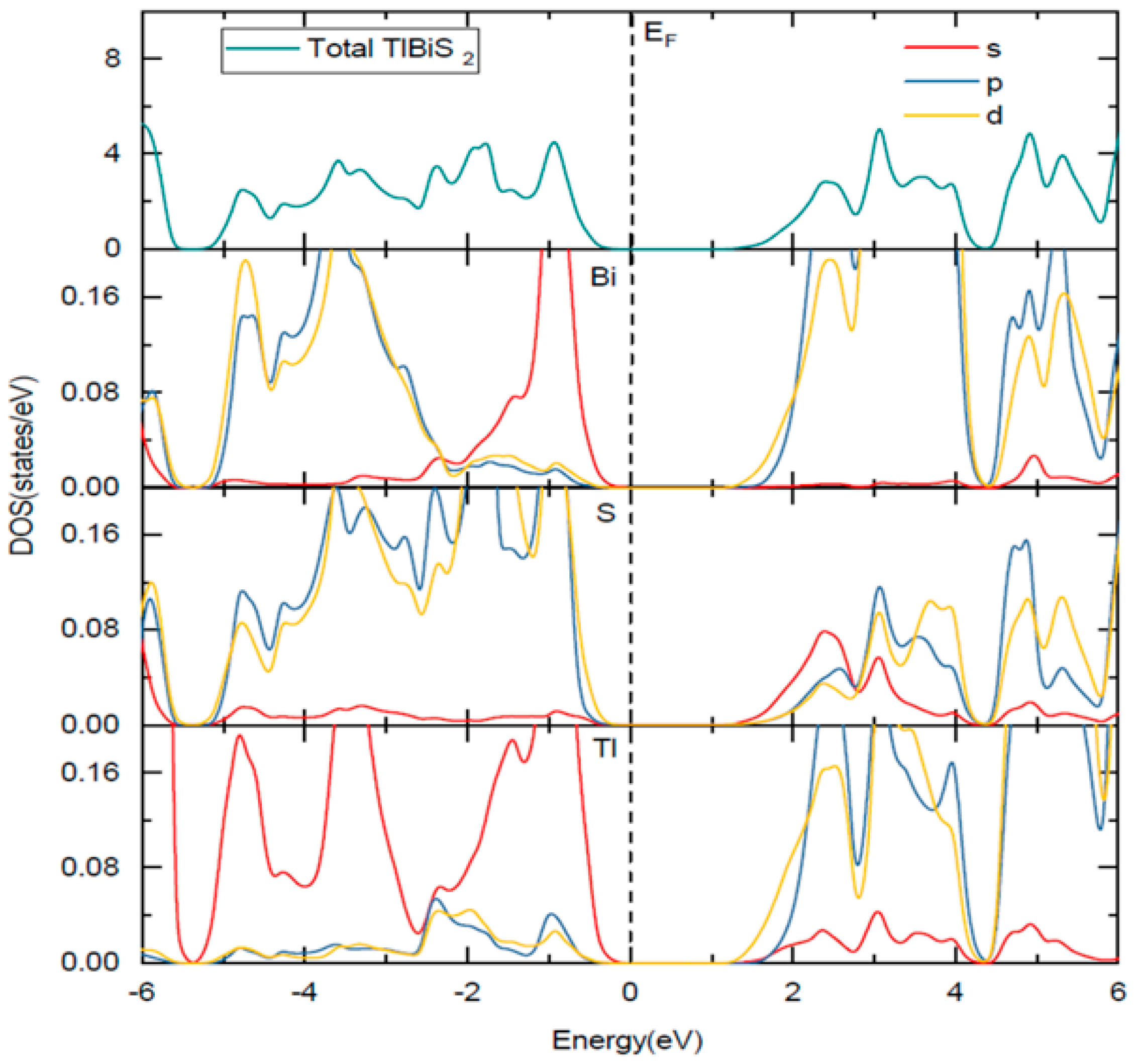
The HSE06 band structure of TlBiS2 is shown in Figure 2a. Both the valence band maximum (VBM) and the conduction band minimum (CBM) are well placed at the Г k-point. This clearly shows that TlBiS2 is a direct band gap semiconductor with valence bands derived from Bi-s, S-p, and Tl-s states, and conduction bands derived from S-s, Bi-p, and Bi-d states (Figure 3). The HSE06 band gap is 1.1 eV for TlBiS2, which is nearly equal to that of Silicon. Bahadur Singh et al., showed that TlBiS2 has GGA band gap of 0.64 eV with direct band gap type at Г k-point [32]. It is important to note that we employed a more accurate HSE06 method compared to the GGA calculation method used by Bahadur Singh et al. [32] and the difference is approximately 0.46 eV. This is as expected because it is well known that calculations using GGA underestimate the band gap value, while the HSE06 screened hybrid functional is very successful in precisely calculating the band gap value. Our calculation shows that we have a band gap of 1.42 eV at F k-point TlBiS2 as shown in Figure 2a. This shows that TlBiS2 well suited for PV applications as optimal band gap for the best performance is 1.4 eV as mentioned earlier [12].
In the case of Ba3BiN, the VBM and CBM are located at Г k-point. Thus, the calculated HSE06 band structure in Figure 2b shows that Ba3BiN is a direct band gap semiconductor with a band gap of 1.29 eV. From the Figure S3 of Supplementary Materials, the valence band derived from Bi-p and hybridized Ni-d states and conduction bands are mainly composed of Bi-s and Ba-s states. According to Imran Ullah et al., Ba3BiN is a direct band gap semiconductor with a band gap of 0.64 eV at Г k-point [33]. The comparison between the present results using HSE06 with the previous results using GGA [33] reveals that the band gap of Ba3BiN is previously underestimated by 0.79 eV. To the best of our knowledge, no HSE06 or experimental studies have been previously reported on Ba3BiN. For Ag2BaS2, the calculated HSE06 band structure in Figure 2c shows that the VBM and CBM are located at the Г k-point. Thus, Ag2BaS2 is a direct band gap semiconductor with a band gap of 1.95 eV. Note that our direct band gap value of 1.95 eV calculated with HSE06 closely matches the previous HSE06 band gap value of 2.01 eV [34] calculated by Aditi Krishnapriyan et al. To the best of our knowledge, no experimental study has been previously reported on Ag2BaS2. From Figure 2b and the Figure S4 of Supplementary Materials, the valence band maximum is derived from S-p states and conduction band derived from Ag-s states. In the case of ZrSO, both the VBM and the CBM are located at Г. Thus, ZrSO is a direct band gap semiconductor with valence bands derived from S-p states, and conduction bands derived from O-s states (Figure S5). The calculated HSE06 band gap between VBM and CBM is 2.60 eV. To the best of our knowledge, no HSE06 and experimental study have previously reported on ZrSO.
3.3. Effective Mass Calculation
We calculate the conductivity effective masses for all four materials; calculated values are listed in Table 2. To study of energy levels in solar devices, calculations of the effective mass (EM) play a crucial role. The conductivity effective masses of electrons and holes deal with the mobility, electrical resistivity, and free-carrier optical response in the semiconductor material used in PV applications. For EM calculation, we have used a finite difference method as implemented in the effective mass calculator (EMC) [35]. For TlBiS2, Ba3BiN, and Ag2BaS2, the EM of holes was found to be heavier than the EM of electrons. This result can be ascribed to the fact that the VBM is less dispersed than the CBM. Prominent PV materials Silicon (Si) and gallium arsenide (GaAs) have EMs of 0.26 me and 0.12 me [36] respectively for electrons. The calculated EM of electrons are 0.154 me, 0.092 me, and 0.149 me for TlBiS2, Ba3BiN, and Ag2BaS2 respectively. Compared to Si, for TlBiS2, Ba3BiN, and Ag2BaS2, the EM of the electron is lower. Hence, the electron mobility in these three compounds is better than that of silicon. However, in the case of ZrSO, the EM of the hole is lighter than the EM of electrons; this is due to CBM being less dispersed than VBM in ZrSO.
3.4. Lattice Dynamic Stability
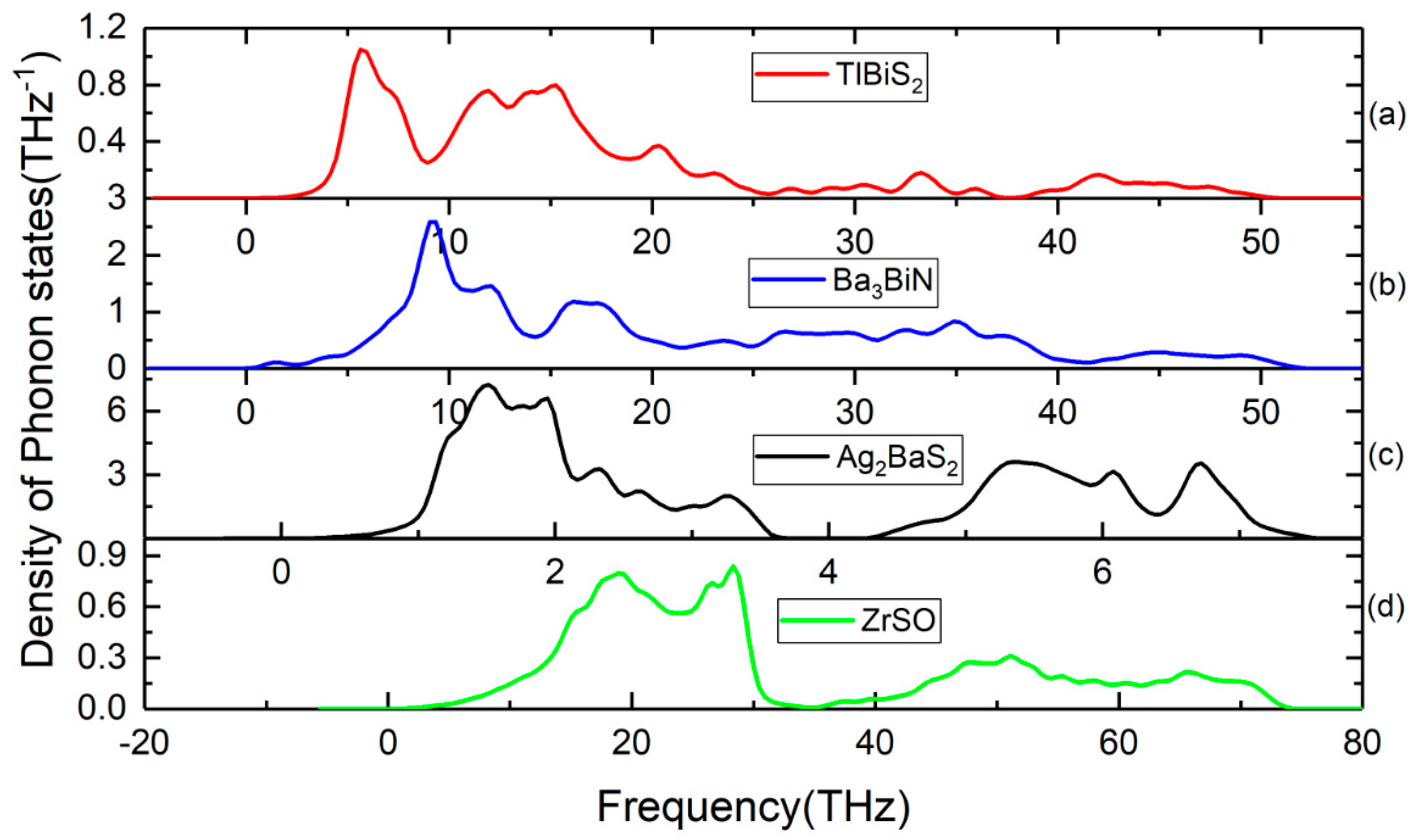
Lattice dynamic calculations have also been performed on TlBiS2, Ba3BiN, Ag2BaS2, and ZrSO under ambient conditions. To validate the dynamical stability of these compounds, the total phonon density of states is calculated at the equilibrium volume. In Figure 4, we displayed their total phonon density of states. No imaginary frequencies were observed, revealing that TlBiS2, Ba3BiN, Ag2BaS2, and ZrSO are dynamically stable. We present the site projected phonon density of states for TlBiS2, Ba3BiN, Ag2BaS2, and ZrSO in Figure 5. The vibrational modes spread over the 2 to 50 THz range in the case of TlBiS2 phase. In the low frequencies region, Tl is dominant over Bi and S. The lattice vibrational modes for the Tl, S, and Bi are present between 3–10, 5–21, and 18–50 THz, respectively. In the case of Ba3BiN, the vibrational modes spread over 0 to 52 THz. The lattice vibrational modes for N, Bi, and Ba are present between 0–19, 2–20 and 3–51 THz, respectively. For Ag2BaS2, the vibrational modes spread over 0.3 to 7.5 THz. The Ag-S and Ba-S stretching modes are present between 1–3 THz. Other Ag-Ba, S-Ag, and S-Ba stretching modes are present between 5–6.5, 5–6.5 and 4.3–7 THz, respectively. The lattice vibrational modes for Ag, Ba, and S are present between 0.3–3.6, 0.3–3.6, and 4.3–7.5 THz, respectively.
In the case of ZrSO, the vibrational modes spread over 2 to 74 THz. The Zr-O and S-O stretching modes are present between 5–30 THz. Other O-Zr and O-S stretching modes are present at 40–65 and 47–60 THz, respectively. The lattice vibrational modes for Zr, S, and O are present between 2–35, 2–35, and 35–74 THz, respectively. The calculated zero-point energy (ZPE) for the TlBiS2, Ba3BiN, Ag2BaS2, and ZrSO phases varies from 0.10 to 1.3 eV/f.u. (see Table 3), and the following ZPE sequence are: Ag2BaS2 < TlBiS2 < ZrSO < Ba3BiN.
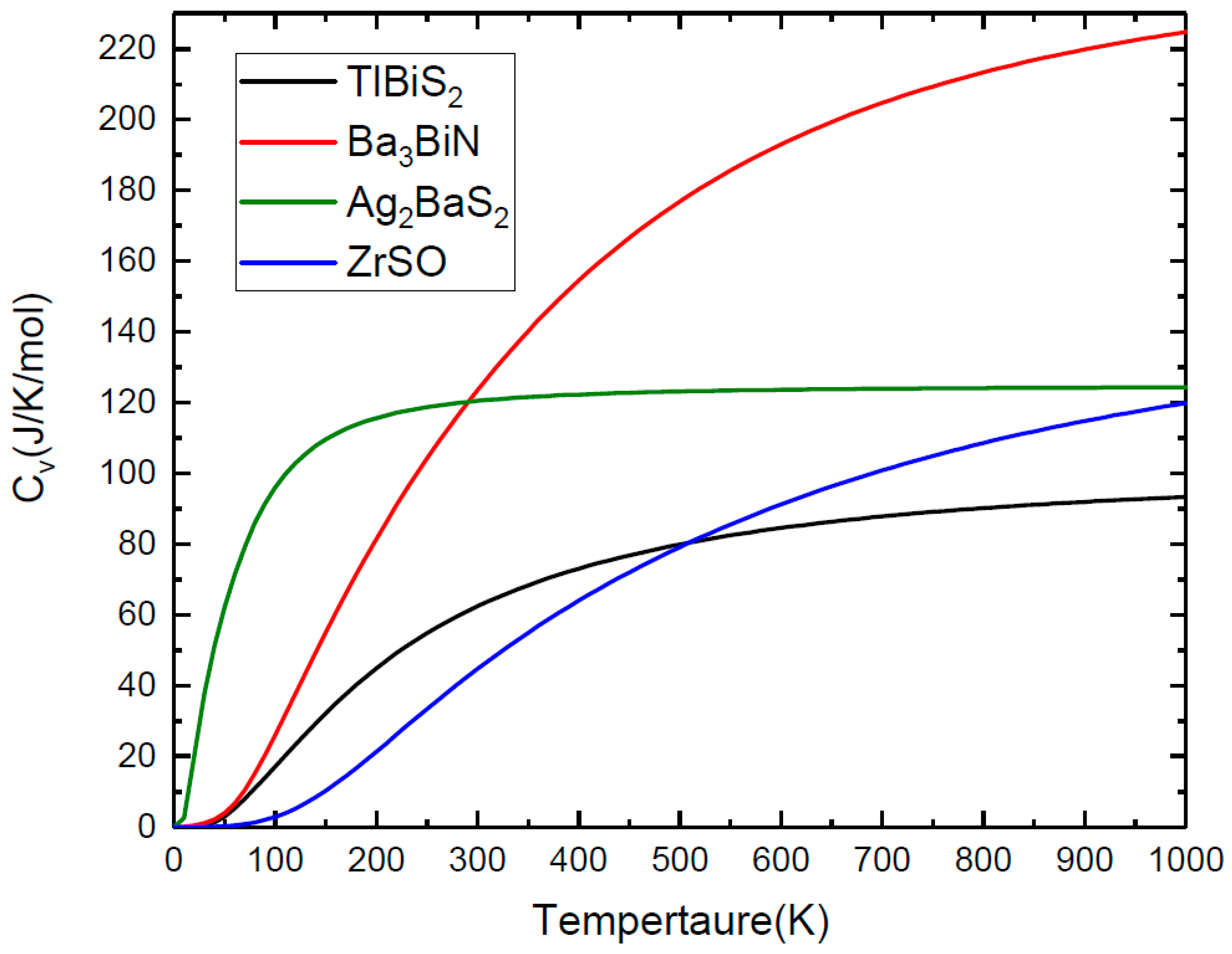
In addition to the dynamic stability, we employ the vibrational density of states to compute the specific heat capacity (Cv) of TlBiS2, Ba3BiN, Ag2BaS2, and ZrSO at constant volume and pressure. The Cv as a function of temperature presented in Figure 6 in the temperature range from 0 K to 1000 K. For TlBiS2, the specific heat capacity increases rapidly below 500 K. The value of Cv is almost constant at 90 J/K/mol for above 500 K. In the case of Ba3BiN, the Cv increases rapidly up to 1000 K. The specific heat capacity increases rapidly below 100 K for Ag2BaS2. The Cv is almost constant at 125 J/K/mol for above 100 K. For ZrSO, the Cv increases from 100 K to 1000 K. The following Cv sequence are: TlBiS2 < ZrSO < Ag2BaS2 < Ba3BiN.
3.5. Mechanical Stability
The mechanical stability of a system is an essential condition to validate the existence of a compound in a given crystalline structure. The elastic constants are typically used to describe the mechanical properties of a system and to estimate its hardness. To validate the mechanical stability of TlBiS2, Ba3BiN, Ag2BaS2, and ZrSO, we calculated the single-crystal elastic constant tensor using the finite strain technique. The elastic constants describe the ability of materials to deform, or conversely, the stress required to maintain a given deformation. Both stresses and strains have three tensile and three shear components. The linear elastic constants form a 6 × 6 symmetric matrices, with 27 independent components, so that (si only) sij = Cij εj (si is stress tensor, Cij is elastic constant matrix, εj (j = 1, 6 in Voigt index) is the strain tensor, and i = 1, …, 6) for small stresses and strains [37].
The stiffness of a crystal against an externally applied strain can be determined from its elastic constants. Any symmetry present in the structure may make some of these components equal, while others may be fixed to zero. The calculated elastic constants of four non-silicon materials listed in Table 4. The elastic constant C44 is a crucial parameter, indirectly describing the indentation hardness of the materials. As shown in Table 4, all the examined compounds have a small C44 value, indicating these materials possess a relatively weak shear strength.
For trigonal structures, the mechanical stability criteria at zero pressure are as follows [38]:
C11 > |C12|, C11 > 0, C33 > 0, C44 > 0
[(C11 + C12) C33 − 2C213] > 0
[(C11 − C12) C44 − 2C214] > 0
In this study, trigonal TlBiS2 and Ag2BaS2 have six independent elastic constants. All the three mechanical stability conditions given in Equations (1)–(3) are satisfied for the TlBiS2 and Ag2BaS2 phases. Hence, this indicates that these two trigonal phase materials are mechanically stable.
For the hexagonal system, the Born stability criteria are [38]:
C44 > 0
C11 − |C12| > 0
[(C11 + C12) C33 − 2C213] > 0
The hexagonal-Ba3BiN has five independent elastic constants. All three conditions for the mechanical stability given in equations 4 to 6 are satisfied for this structure, and this finding indicates that hexagonal-Ba3BiN phases are mechanically stable.
The mechanical stability criteria for the tetragonal phase are given by [38]:
C11 − C12
2(C11 + C12) + C33 + 4C13
C44 > 0, C66 > 0
C11 + C12 − 2C13 > 0
ZrSO has a tetragonal structure, and thus, six independent elastic constants. All three conditions for mechanical stability given in Equations (7)–(10) are satisfied for this structure. Hence, the tetragonal-ZrSO phase is mechanically stable at ambient conditions. Equations (1)–(9) and Table 4 validated the mechanical stability criteria for the crystal under ambient conditions. This outcome is consistent with the phonon calculations presented in Section 3.4.
From the calculated elastic constants, the bulk (Bv, BR) and shear moduli (Gv, GR) are calculated from Voigt–Reuss–Hill approximations [39,40]. The bulk and shear moduli contain information related to the hardness of the material under various types of deformation. Generally, very hard materials hold very large bulk and shear moduli to support the volume decrease and to restrict deformation, respectively [41]. From Table 4, it can be identified that the listed TlBiS2, Ba3BiN, and Ag2BaS2 phases have a smaller bulk modulus than ZrSO (181.403 GPa). This indicates that ZrSO is more difficult to compress than the other three materials. Among these compounds, the bulk modulus sequence is: ZrSO > Ag2BaS2 > TlBiS2 > Ba3BiN. As we know, the shear modulus is more closely-connected to hardness than the bulk modulus. From Table 4, the shear modulus of ZrSO is higher than the other three compounds. Hence, the hardness of the tetragonal-ZrSO phase is higher than trigonal-TlBiS2, hexagonal-Ba3BiN, and trigonal-Ag2BaS2. Among these compounds, the shear modulus trend is ZrSO > TlBiS2 > Ag2BaS2 > Ba3BiN. Seemingly, the bulk and shear moduli of Ba3BiN are smaller than other compounds. Thus, Ba3BiN is easy to compress and is the softest of the examined materials.
The parameter G/B can be introduced, in which G indicates the shear modulus and B the bulk modulus. The low/high of G/B value is connected with the ductility or brittleness of the materials. The critical G/B value that separates the ductile and brittle materials is 0.5 [41]. If the G/B value of materials is smaller than 0.5, then those materials are ductile; otherwise they are brittle. From Table 4, the calculated G/B values of all four materials are greater than 0.5, indicating that these materials are ductile. Next, the value of Poisson’s ratio is indicative of the degree of directionality of the covalent bonding. Among these compounds, the small Poisson’s ratio (0.13) for hexagonal-Ba3BiN indicates a high degree of covalent bonding. All these phases present a very scattered Young’s (varying from 29 to 339 GPa). The compressibility value of these phases suggests that these compounds, with the exception of ZrSO, are very soft materials. The compressibility sequence is ZrSO < Ag2BaS2 < TlBiS2 < Ba3BiN.
3.6. Optical Properties
The optical behavior of a compound has a major impact on its properties for photovoltaic applications. Optical dielectric function ε(ω) = ε1(ω) + ιε2(ω) is the fundamental quantity that describes the optical properties of a material. It describes the response of a material to a radiated electromagnetic field and the propagation of the field inside the material. The dielectric function is dependent on the frequency of electromagnetic field, and it is connected to the interaction between photons and electrons. The absorption coefficient of the material is dependent on the imaginary part, ε2(ω), and it can be derived from the inter-band optical transitions by summing over the unoccupied states, using the equation [42,43],
where the indices α, β are the Cartesian components, is the volume of the primitive cell, q denotes the Bloch vector of the incident wave, c and v are the conduction and valence band states respectively, k is the Bloch wave vector, wk denotes the k-point weight, is a Dirac delta function, uck is the cell periodic part of the orbital at k-point k, refers to the energy of the conduction band, and refers to the energy of the valence band. The real part ε1(ω) of the dielectric function can be derived from ε2(ω) using the Kramer-Kronig relationship [42,43]
where P indicates the principal value, η is the complex shift. All the frequency dependent linear optical properties, such as the absorption coefficients α(ω), can be calculated from ε1(ω) and ε2(ω) [42,43].
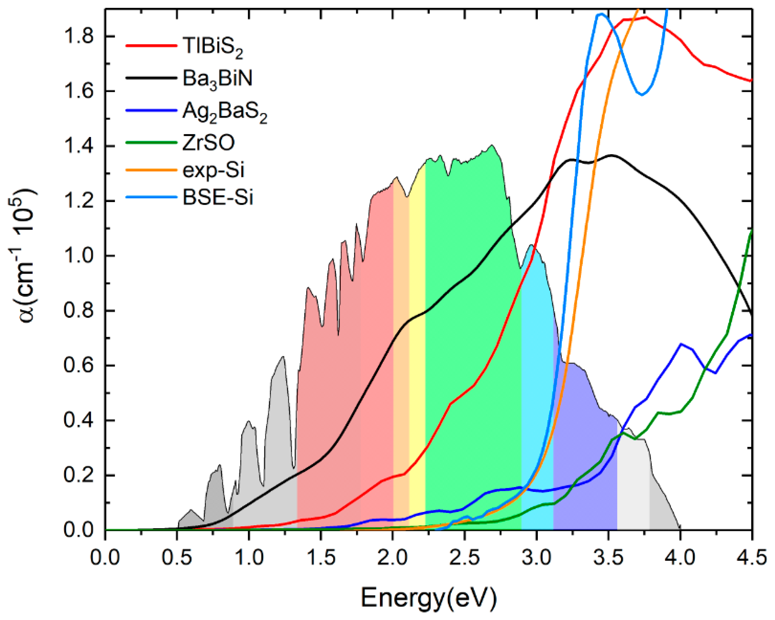
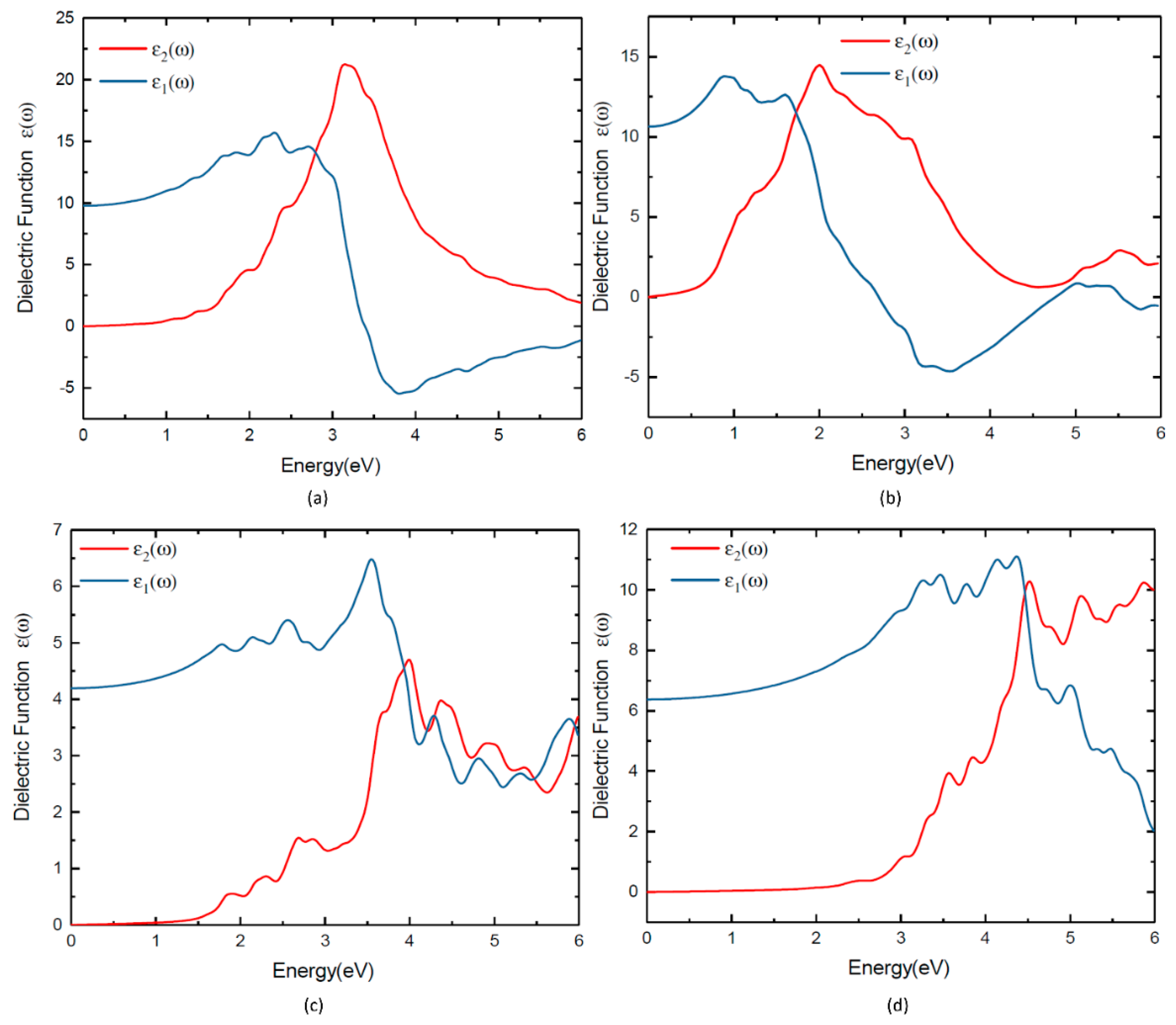
Experimental absorption spectra are in agreement with the inclusion of excitonic effects treated within the Bethe-Salpeter equation (BSE) in general [44,45,46]. By averaging multiple grids using BSE, the calculated the dielectric function of these four materials can be further improved. The calculated ε2(ω) of the dielectric function and the absorption coefficients of TlBiS2, Ba3BiN, Ag2BaS2, and ZrSO are presented in Figure 7 and Figure 8, respectively. From the directional dependency of ε1(ω) and ε2(ω), trigonal-TlBiS2 is highly isotropic, whereas hexagonal-Ba3BiN, trigonal-Ag2BaS2, and tetragonal-ZrSO are less anisotropic. We present the average of the real and imaginary parts of the dielectric function for the four examined compounds.
In Figure 7, we plotted both real and imaginary part of the dielectric function of (a) TlBiS2, (b) Ba3BiN, (c) Ag2BaS2, and (d) ZrSO is plotted against the photon energy. The optical absorption coefficients of all these materials were calculated using BSE and plotted in Figure 8. For a comparison, we have also plotted both the experimentally-verified [47] and the BSE-calculated [19] values for the optical absorption coefficient of silicon in the same Figure 8. Absorption in a material take place only when the incident photon has more energy than energy band gap of the material. Since TlBiS2 is a direct band gap material with a band gap of 1.10 eV, we notice the absorption to occur when the energy of the photon is around 1.08 eV, as shown in Figure 8. It is clearly seen in Figure 8 that there are absorption peaks at 1.32 eV, 1.93 eV, 2.45 eV, and 3.6 eV. The absorption coefficient of TlBiS2 has a maximum value when the photon energy is about 3.6 eV. For silicon, the absorption coefficient becomes appreciably different from zero after 2.5 eV, and it is still not very large up to 3 eV. This phenomenon can be attributed to the indirect band gap of silicon that leads to low absorption in the visible region. We observe that the absorption coefficient of TlBiS2 is superior to silicon in the visible region. This is due to the direct band gap at Г and F k-points that prevails in the TlBiS2.
In the case of hexagonal-Ba3BiN, the dielectric function is calculated at the BSE level (Figure 7b). Due to the narrow band gap, Ba3BiN can absorb photons mostly in the visible region. The HSE06 band gap is 1.29 eV, and it is direct. Therefore, Ba3BiN exhibits an absorption which rapidly increases after 1.26 eV. It can be observed that the absorption peaks of Ba3BiN are at 2.08 eV, 3.21 eV, and 3.5 eV (Figure 8). The absorption coefficient of Ba3BiN reaches its maximum when the photon energy is about 3.5 eV. From Figure 8, it can be noted that the optical absorption of Ba3BiN occurs in the visible region, with higher values compared to other materials considered. The reason behind the high optical absorption of Ba3BiN is due to the direct band gap of 1.29 eV. From Figure 8, it can be observed that absorption peaks of Ag2BaS2 are at 1.94 eV, 2.24 eV, 2.7 eV, and 3.6 eV. Ag2BaS2 seems to have a lower absorption coefficient than TlBiS2 and Ba3BiN in the visible region. However, Ag2BaS2 exhibits better optical absorption than silicon in the visible region. In the same Figure 8, we notice that absorption peaks of ZrSO start at 2.5 eV. The absorption peaks of ZrSO are also observed at 2.6 eV, 3 eV, and 3.59 eV. Among these four non-silicon materials, the absorption coefficient of ZrSO is smaller than those of the other three; this is due to the wideband gap of ZrSO.
4. Conclusions
We employed band gap calculations based on GGA on a pool of 1000 materials in order to identify twenty-seven possible candidates for photovoltaic applications. Among these candidates, four promising materials that had direct band gaps were chosen, and in-depth analysis was carried out to check the utility of these compounds for photovoltaic applications. We have presented a set of first-principle calculations employing the hybrid functional HSE06 and utilized to compute the electronic structures and effective masses of the four chosen materials, namely, TlBiS2, Ba3BiN, Ag2BaS2, and ZrSO. The BSE method was employed to calculate the optical properties. Our study provided rational insights into the electronic structure and optical properties of these four non-silicon materials. These four materials exhibit a direct band gap in the range of 1.10 eV to 2.60 eV.
The main advantage with TlBiS2, Ba3BiN, and Ag2BaS2 is that all three materials have direct band gaps and higher absorption coefficients than the widely-used photovoltaic material silicon in the visible region. Among these three materials, TlBiS2 and Ba3BiN have better optical properties than Ag2BaS2. ZrSO is the least preferable photovoltaic material because of the fact that its absorption properties are inferior to those of silicon. Nevertheless, we have shown that there is a significant difference in the GGA and HSE06 calculation for ZrSO. The phonon calculations revealed that TlBiS2, Ba3BiN, Ag2BaS2, and ZrSO are dynamically stable, as no imaginary frequencies were observed. Our elastic constant calculations illustrate that the compounds are mechanically stable. The calculated G/B values are greater than 0.5, confirming the brittle nature of these materials. Our detailed studies of the electronic, structural stability, mechanical stability and optical properties of these four materials show them to be potential candidates for photovoltaic application.
Supplementary Materials
The following are available online at https://www.mdpi.com/1996-1944/11/10/2006/s1, Table S1: Calculated GGA band gap values for 30 compounds with lattice parameters; Table S2: Calculated structural parameters and atomic positions of TlBiS2, Ba3BiN, Ag2BaS2, and ZrSO; Figure S1: Calculated total energy as a function of unit cell volume for cubic- and tetragonal-ZrSO; Figure S2: Crystal structures for (a) cubic-ZrSO; (b) tetragonal-ZrSO. The legends for the different kinds of atoms shown in the illustration; Figure S3: Total and site projected density of states of Ba3BiN. The Fermi level is set to zero and marked by a vertical dotted line; Figure S4: Total and site projected density of states of Ag2BaS2. The Fermi level is set to zero and marked by a vertical dotted line; Figure S5: Total and site projected density of states of ZrSO. The Fermi level is set to zero and marked by a vertical dotted line.
Author Contributions
Conceptualization, M.R., D.V. and P.V.; Methodology, M.R., D.V. and P.V.; Software, M.R., P.V. and D.V.; Validation, P.V., M.R., F.B. and D.V.; Formal Analysis, M.R.; Investigation, M.R., D.V. and P.V.; Resources, M.R., P.V.; Data Curation, M.R. and P.V.; Writing-Original Draft Preparation, M.R.; Writing-Review & Editing, D.V., P.V. and F.B.; Visualization, M.R. and P.V.; Supervision, D.V., P.V.; Project Administration, D.V.; Funding Acquisition, D.V.
Funding
This research was funded by Western Norway University of Applied Sciences grant number 23300.
Acknowledgments
The authors gratefully acknowledge the Western Norway University of Applied Sciences for financially supporting the project (23300) and UNINETT Sigma2 for computing facilities of project numbers NN2867K and NN2875K, which have been used to conduct the calculations presented in this article, and further acknowledge Vishnukanthan Venkatachalapathy for fruitful discussions.
Conflicts of Interest
The authors declare no conflict of interest.
References
- Unold, T.; Schock, H.-W. Nonconventional (non-silicon-based) photovoltaic materials. Annu. Rev. Mater. Res. 2011, 41, 297–321. [Google Scholar] [CrossRef]
- Shockley, W.; Queisser, H.J. Detailed balance limit of efficiency of p-n junction solar cells. J. Appl. Phys. 1961, 32, 510–519. [Google Scholar] [CrossRef]
- Goetzberger, A.; Hebling, C.; Schock, H.-W. Photovoltaic materials, history, status and outlook. Mater. Sci. Eng. R Rep. 2003, 40, 1–46. [Google Scholar] [CrossRef]
- Bube, R.H. Materials for photovoltaics. Annu. Rev. Mater. Sci. 1990, 20, 19–50. [Google Scholar] [CrossRef]
- Birkmire, R.W.; Eser, E. Polycrystalline thin film solar cells: Present status and future potential. Annu. Rev. Mater. Sci. 1997, 27, 625–653. [Google Scholar] [CrossRef]
- Mitchell, K.W. Status of new thin-film photovoltaic technologies. Annu. Rev. Mater. Sci. 1982, 12, 401–413. [Google Scholar] [CrossRef]
- Boer, K.; Rothwarf, A. Materials for solar photovoltaic energy conversion. Annu. Rev. Mater. Sci. 1976, 6, 303–333. [Google Scholar] [CrossRef]
- Rasukkannu, M.; Velauthapillai, D.; Vajeeston, P. Computational modeling of novel bulk materials for the intermediate-band solar cells. ACS Omega 2017, 2, 1454–1462. [Google Scholar] [CrossRef]
- Rasukkannu, M.; Velauthapillai, D.; Vajeeston, P. A first-principle study of the electronic, mechanical and optical properties of inorganic perovskite Cs2SnI6 for intermediate-band solar cells. Mater. Lett. 2018, 218, 233–236. [Google Scholar] [CrossRef]
- Hellenbrandt, M. The inorganic crystal structure database (ICSD)—Present and future. Crystallogr. Rev. 2004, 10, 17–22. [Google Scholar] [CrossRef]
- Ponniah, V. Density Functional Theory Based Database (DFTBD); University of Oslo: Oslo, Norway, 2013. [Google Scholar]
- Rasukkannu, M.; Velauthapillai, D.; Ponniah, V. A promising high-efficiency photovoltaic alternative non-silicon material: A first-principle investigation. Scr. Mater. 2018, 156, 134–137. [Google Scholar] [CrossRef]
- Kresse, G.; Furthmüller, J. Efficient iterative schemes for ab initio total-energy calculations using a plane-wave basis set. Phys. Rev. B 1996, 54, 11169. [Google Scholar] [CrossRef]
- Perdew, J.P.; Burke, K.; Ernzerhof, M. Generalized gradient approximation made simple. Phys. Rev. Lett. 1996, 77, 3865. [Google Scholar] [CrossRef] [PubMed]
- Dudarev, S.; Botton, G.; Savrasov, S.Y.; Szotek, Z.; Temmerman, W.; Sutton, A. Electronic structure and elastic properties of strongly correlated metal oxides from first principles: LSDA+ U, SIC-LSDA and EELS study of UO2 and NiO. Phys. Status Solidi A 1998, 166, 429–443. [Google Scholar] [CrossRef]
- Kresse, G.; Furthmüller, J. Efficiency of ab-initio total energy calculations for metals and semiconductors using a plane-wave basis set. Comput. Mater. Sci. 1996, 6, 15–50. [Google Scholar] [CrossRef]
- Liechtenstein, A.; Anisimov, V.; Zaanen, J. Density-functional theory and strong interactions: Orbital ordering in Mott-Hubbard insulators. Phys. Rev. B 1995, 52, R5467. [Google Scholar] [CrossRef]
- Heyd, J.; Scuseria, G.E. Efficient hybrid density functional calculations in solids: Assessment of the Heyd–Scuseria–Ernzerhof screened Coulomb hybrid functional. J. Chem. Phys. 2004, 121, 1187–1192. [Google Scholar] [CrossRef] [PubMed]
- Paier, J.; Marsman, M.; Kresse, G. Dielectric properties and excitons for extended systems from hybrid functionals. Phys. Rev. B 2008, 78, 121201. [Google Scholar] [CrossRef]
- Aroyo, M.I.; Perez-Mato, J.M.; Capillas, C.; Kroumova, E.; Ivantchev, S.; Madariaga, G.; Kirov, A.; Wondratschek, H. Bilbao Crystallographic Server: I. Databases and crystallographic computing programs. Z. Krist. Cryst. Mater. 2006, 221, 15–27. [Google Scholar] [CrossRef]
- Aroyo, M.I.; Kirov, A.; Capillas, C.; Perez-Mato, J.; Wondratschek, H. Bilbao Crystallographic Server. II. Representations of crystallographic point groups and space groups. Acta Crystallogr. Sect. A Found. Crystallogr. 2006, 62, 115–128. [Google Scholar] [CrossRef] [PubMed] [Green Version]
- Aroyo, M.I.; Perez-Mato, J.; Orobengoa, D.; Tasci, E.; De La Flor, G.; Kirov, A. Crystallography online: Bilbao crystallographic server. Bulg. Chem. Commun. 2011, 43, 183–197. [Google Scholar]
- Togo, A.; Oba, F.; Tanaka, I. First-principles calculations of the ferroelastic transition between rutile-type and CaCl2-type SiO2 at high pressures. Phys. Rev. B 2008, 78, 134106. [Google Scholar] [CrossRef]
- Togo, A.; Tanaka, I. First principles phonon calculations in materials science. Scr. Mater. 2015, 108, 1–5. [Google Scholar] [CrossRef] [Green Version]
- Monkhorst, H.J.; Pack, J.D. Special points for Brillouin-zone integrations. Phys. Rev. B 1976, 13, 5188. [Google Scholar] [CrossRef]
- Shannon, R.D. Revised effective ionic radii and systematic studies of interatomic distances in halides and chalcogenides. Acta Crystallogr. Sect. A Cryst. Phys. Diffr. Theor. Gen. Crystallogr. 1976, 32, 751–767. [Google Scholar] [CrossRef] [Green Version]
- Gäbler, F.; Kirchner, M.; Schnelle, W.; Schwarz, U.; Schmitt, M.; Rosner, H.; Niewa, R. (Sr3N) E and (Ba3N) E (E = Sb, Bi): Synthesis, crystal structures, and physical properties. Z. Anorg. Allg. Chem. 2004, 630, 2292–2298. [Google Scholar] [CrossRef]
- Steinbrenner, U.; Simon, A. Ba3N–a new binary nitride of an alkaline earth metal. Z. Anorg. Allg. Chem. 1998, 624, 228–232. [Google Scholar] [CrossRef]
- Bronger, W.; Lenders, B.; Huster, J. BaAg2S2, ein Thioargentat im CaAl2Si2-Strukturtyp. Z. Anorg. Allg. Chem. 1997, 623, 1357–1360. [Google Scholar] [CrossRef]
- McCullough, J.D.; Brewer, L.; Bromley, L. The crystal structure of zirconium oxysulfide, ZrOS. Acta Crystallogr. 1948, 1, 287–289. [Google Scholar] [CrossRef] [Green Version]
- Jellinek, F.; Songstad, J.; Viljanto, J.; Seppälä, P.; Theander, O.; Flood, H. A Tetragonal Form of Zirconium Oxide Sulfide, ZrOS. Acta Chem. Scand. 1962, 16, 791–792. [Google Scholar] [CrossRef]
- Singh, B.; Lin, H.; Prasad, R.; Bansil, A. Topological phase transition and quantum spin Hall state in TlBiS2. J. Appl. Phys. 2014, 116, 033704. [Google Scholar] [CrossRef]
- Ullah, I.; Murtaza, G.; Khenata, R.; Mahmood, A.; Muzzamil, M.; Amin, N.; Saleh, M. Structural and Optoelectronic Properties of X3ZN (X = Ca, Sr, Ba; Z = As, Sb, Bi) Anti-Perovskite Compounds. J. Electron. Mater. 2016, 45, 3059–3068. [Google Scholar] [CrossRef]
- Krishnapriyan, A.; Barton, P.T.; Miao, M.; Seshadri, R. First-principles study of band alignments in the p-type hosts BaM2X2 (M = Cu, Ag; X = S, Se). J. Phys. Condens. Matter 2014, 26, 155802. [Google Scholar] [CrossRef] [PubMed]
- Fonari, A.; Sutton, C. Effective Mass Calculator for Semiconductors. 2015. Available online: https://github.com/afonari/emc (accessed on 2 July 2018).
- Van Zeghbroeck, B. Principles of Semiconductor Devices; Colarado University: Denver, CO, USA, 2004. [Google Scholar]
- Ashcroft, N. ND Mermin Solid State Physics WB Saunders Company; Saunders College: Philadelphia, PA, USA, 1976. [Google Scholar]
- Nye, J.F. Physical Properties of Crystals: Their Representation by Tensors and Matrices; Oxford University Press: Oxford, UK, 1985. [Google Scholar]
- Hill, R. The elastic behaviour of a crystalline aggregate. Proc. Phys. Soc. Sect. A 1952, 65, 349. [Google Scholar] [CrossRef]
- Reuss, A. Berechnung der fließgrenze von mischkristallen auf grund der plastizitätsbedingung für einkristalle. ZAMM J. Appl. Math. Mech. 1929, 9, 49–58. [Google Scholar] [CrossRef]
- Pugh, S. XCII. Relations between the elastic moduli and the plastic properties of polycrystalline pure metals. Lond. Edinb. Dublin Philos. Mag. J. Sci. 1954, 45, 823–843. [Google Scholar] [CrossRef]
- Gajdoš, M.; Hummer, K.; Kresse, G.; Furthmüller, J.; Bechstedt, F. Linear optical properties in the projector-augmented wave methodology. Phys. Rev. B 2006, 73, 045112. [Google Scholar] [CrossRef]
- Yang, L.-M.; Vajeeston, P.; Ravindran, P.; Fjellvåg, H.; Tilset, M. Revisiting isoreticular MOFs of alkaline earth metals: A comprehensive study on phase stability, electronic structure, chemical bonding, and optical properties of A–IRMOF-1 (A = Be, Mg, Ca, Sr, Ba). Phys. Chem. Chem. Phys. 2011, 13, 10191–10203. [Google Scholar] [CrossRef] [PubMed]
- Albrecht, S.; Reining, L.; Del Sole, R.; Onida, G. Ab initio calculation of excitonic effects in the optical spectra of semiconductors. Phys. Rev. Lett. 1998, 80, 4510. [Google Scholar] [CrossRef]
- Bokdam, M.; Sander, T.; Stroppa, A.; Picozzi, S.; Sarma, D.; Franchini, C.; Kresse, G. Role of polar phonons in the photo excited state of metal halide perovskites. Sci. Rep. 2016, 6, 28618. [Google Scholar] [CrossRef] [PubMed]
- Rohlfing, M.; Louie, S.G. Electron-hole excitations in semiconductors and insulators. Phys. Rev. Lett. 1998, 81, 2312. [Google Scholar] [CrossRef]
- Aspnes, D.E.; Studna, A. Dielectric functions and optical parameters of Si, Ge, GaP, GaAs, GaSb, InP, InAs, and InSb from 1.5 to 6.0 ev. Phys. Rev. B 1983, 27, 985. [Google Scholar] [CrossRef]
Figure 1.
Crystal structures for (a) TlBiS2; (b) Ba3BiN; (c) Ag2BaS2; (d) Tetragonal-ZrSO. The illustration shows the legends for the different type of atoms.
Figure 1.
Crystal structures for (a) TlBiS2; (b) Ba3BiN; (c) Ag2BaS2; (d) Tetragonal-ZrSO. The illustration shows the legends for the different type of atoms.

Figure 2.
Calculated electronic band structure (using HSE06) of (a) TlBiS2(Colour code: red line—Bi, green line—S, blue—Tl), (b) Ba3BiN (Colour code: red line—Ba, green line—Bi, blue—N), (c) Ag2BaS2 (Colour code: red line—S, green line—Ag, blue—Ba) and (d) ZrSO (Colour code: red line—O, green line—S, blue—Zr). The Fermi level is set to zero.

Figure 3.
Total and site projected density of states of TlBiS2. The Fermi level is set to zero. The Fermi level is set to zero and marked by a vertical dotted line.
Figure 3.
Total and site projected density of states of TlBiS2. The Fermi level is set to zero. The Fermi level is set to zero and marked by a vertical dotted line.

Figure 4.
Calculated total phonon density of states for (a) TlBiS2, (b) Ba3BiN, (c) Ag2BaS2, and (d) ZrSO phases.
Figure 4.
Calculated total phonon density of states for (a) TlBiS2, (b) Ba3BiN, (c) Ag2BaS2, and (d) ZrSO phases.

Figure 5.
Calculated site projected phonon density of states for (a) TlBiS2, (b) Ba3BiN, (c) Ag2BaS2, (d) ZrSO.
Figure 5.
Calculated site projected phonon density of states for (a) TlBiS2, (b) Ba3BiN, (c) Ag2BaS2, (d) ZrSO.
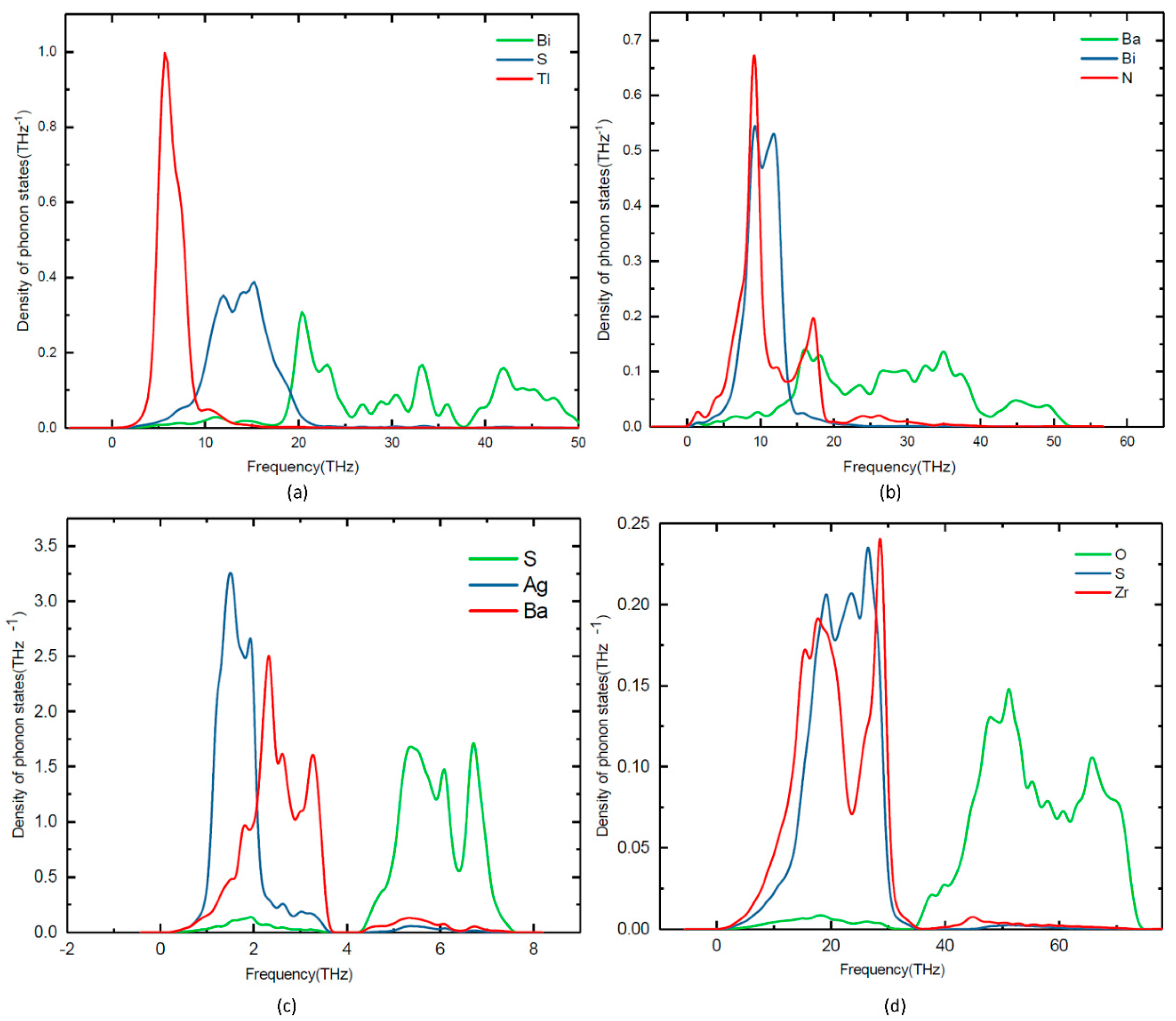
Figure 6.
The heat capacity at constant volume as a function of temperature from zero up to 1000 K.

Figure 7.
Dielectric function of (a) TlBiS2, (b) Ba3BiN, (c) Ag2BaS2 and (d) ZrSO.

Figure 8.
Optical absorption coefficients of TlBiS2, Ba3BiN, Ag2BaS2 and ZrSO. For comparison, we plotted the silicon optical absorption coefficient (color code: orange—experimental absorption coefficient of Si, navy blue—BSE calculation of Si).
Figure 8.
Optical absorption coefficients of TlBiS2, Ba3BiN, Ag2BaS2 and ZrSO. For comparison, we plotted the silicon optical absorption coefficient (color code: orange—experimental absorption coefficient of Si, navy blue—BSE calculation of Si).

Table 1.
Calculated GGA and HSE06 band gap values, type of band gap for TlBiS2, Ba3BiN, Ag2BaS2, and ZrSO phases.
Table 1.
Calculated GGA and HSE06 band gap values, type of band gap for TlBiS2, Ba3BiN, Ag2BaS2, and ZrSO phases.
| Compounds | GGA (eV) | HSE06 (eV) | Type of Band Gap |
|---|---|---|---|
| TlBiS2 | 0.505 | 1.10 | direct |
| Ba3BiN | 0.679 | 1.29 | direct |
| Ag2BaS2 | 0.716 | 1.95 | direct |
| ZrSO | 0.891 | 2.60 | direct |
Table 2.
The calculated effective mass of non-silicon compounds. m*lh, m*hh and m*e are the effective masses of light holes, heavy holes and electrons, respectively. me is the mass of the electron.
Table 2.
The calculated effective mass of non-silicon compounds. m*lh, m*hh and m*e are the effective masses of light holes, heavy holes and electrons, respectively. me is the mass of the electron.
| Serial No. | Plane Directions | Compound | m*lh × me | m*hh × me | m*e × me |
|---|---|---|---|---|---|
| 1. | 110 | TlBiS2 | 0.182 | 0.224 | 0.154 |
| 2. | 110 | Ba3BiN | 0.016 | 0.165 | 0.092 |
| 3. | 110 | Ag2BaS2 | 0.150 | 0.728 | 0.149 |
| 4. | 110 | ZrSO | 0.308 | 0.482 | 0.361 |
Table 3.
Computational details for the phonon calculation (supercell size, number of atoms), calculated zero-point energy (ZPE) and information on dynamical stability based on phonon density of states for TlBiS2, Ba3BiN, Ag2BaS2, and ZrSO phases.
Table 3.
Computational details for the phonon calculation (supercell size, number of atoms), calculated zero-point energy (ZPE) and information on dynamical stability based on phonon density of states for TlBiS2, Ba3BiN, Ag2BaS2, and ZrSO phases.
| Compounds | Supercell Size | Number of Atoms | ZPE (eV) | Dynamical Stability |
|---|---|---|---|---|
| TlBiS2 | 2 × 2 × 2 | 32 | 0.4045 | stable |
| Ba3BiN | 2 × 2 × 2 | 80 | 1.3050 | stable |
| Ag2BaS2 | 2 × 2 × 2 | 40 | 0.1093 | stable |
| ZrSO | 2 × 2 × 2 | 48 | 1.2100 | stable |
Table 4.
The calculated single-crystal elastic constants Cij (in GPa), bulk modulus B (in GPa), shear modulus G (in GPa), Poisson’s ratio (σ), Young’s modulus E (in GPa), compressibility (GPa−1), Ductility for TlBiS2, Ba3BiN, Ag2BaS2 and ZrSO phases. Subscript V illustrates the Voigt bound, R indicates the Reuss bound and VRH indicates the Hill average.
| Properties | TlBiS2 | Ba3BiN | Ag2BaS2 | ZrSO |
|---|---|---|---|---|
| Cij | C11 = 63.47 C12 = 34.68 C13 = 27.49 C14 = 0.608 C33 = 88.90 C44 = 28.90 | C11 = 56.604 C12 = 14.1 C13 = 7.947 C33 = 75.35 C44 = 21.20 | C11 = 84.61 C12 = 31.538 C13 = 34.611 C14 = 0.0732 C33 = 89.994 C44 = 26.642 C66 = 14.590 | C11 = 293.04 C12 = 133.66 C13 = 118.96 C33 = 303.06 C44 = 100.64 C66 = 91.94 |
| BV | 44.85 | 27.762 | 51.59 | 181.407 |
| BR | 44.46 | 27.5620 | 51.28 | 181.39 |
| BVRH | 44.65 | 27.662 | 51.34 | 181.403 |
| GV | 54.99 | 47.7264 | 53.45 | 194.92 |
| GR | 21.08 | 5.70729 | 19.24 | 90.88 |
| GVRH | 38.04 | 26.716 | 36.35 | 142.90 |
| Ductility | 0.852 | 0.96 | 0.708 | 0.7877 |
| σ | 0.168 | 0.1346 | 0.213 | 0.188 |
| E | 89 | 61 | 29 | 339 |
| compressibility | 0.022 | 0.04 | 0.02 | 0.0055 |
© 2018 by the authors. Licensee MDPI, Basel, Switzerland. This article is an open access article distributed under the terms and conditions of the Creative Commons Attribution (CC BY) license (http://creativecommons.org/licenses/by/4.0/).
Share and Cite
MDPI and ACS Style
Rasukkannu, M.; Velauthapillai, D.; Bianchini, F.; Vajeeston, P. Properties of Novel Non-Silicon Materials for Photovoltaic Applications: A First-Principle Insight. Materials 2018, 11, 2006. https://doi.org/10.3390/ma11102006
AMA Style
Rasukkannu M, Velauthapillai D, Bianchini F, Vajeeston P. Properties of Novel Non-Silicon Materials for Photovoltaic Applications: A First-Principle Insight. Materials. 2018; 11(10):2006. https://doi.org/10.3390/ma11102006
Chicago/Turabian StyleRasukkannu, Murugesan, Dhayalan Velauthapillai, Federico Bianchini, and Ponniah Vajeeston. 2018. "Properties of Novel Non-Silicon Materials for Photovoltaic Applications: A First-Principle Insight" Materials 11, no. 10: 2006. https://doi.org/10.3390/ma11102006
Note that from the first issue of 2016, this journal uses article numbers instead of page numbers. See further details here.