Article

Steering the Properties of MoOx Hole Transporting Layers in OPVs and OLEDs: Interface Morphology vs. Electronic Structure

1
Institute for Materials Research (IMO‐IMOMEC), Inorganic and Physical Chemistry, Hasselt University, Martelarenlaan 42, 3500 Hasselt, Belgium
2
IMEC vzw, division IMOMEC, Agoralaan Building D, 3590 Diepenbeek, Belgium
3
Institute for Materials Research (IMO‐IMOMEC), Engineering Materials and Applications, Hasselt University, Wetenschapspark 1, 3590 Diepenbeek, Belgium
4
Institute for Materials Research (IMO‐IMOMEC), Design and Synthesis of Organic Semiconductors, Hasselt University, Martelarenlaan 42, 3500 Hasselt, Belgium
5
Institute for Materials Research (IMO‐IMOMEC), Hasselt University, Wetenschapspark 1, 3590 Diepenbeek, Belgium
6
Flanders make vzw, Oude Diestersebaan 133, 3920 Lommel, Belgium
*
Author to whom correspondence should be addressed.
Materials 2017, 10(2), 123; https://doi.org/10.3390/ma10020123
Submission received: 19 December 2016 / Accepted: 27 January 2017 / Published: 30 January 2017
(This article belongs to the Special Issue Highly Ordered Organic Thin Films)

Abstract

:
The identification, fine-tuning, and process optimization of appropriate hole transporting layers (HTLs) for organic solar cells is indispensable for the production of efficient and sustainable functional devices. In this study, the optimization of a solution-processed molybdenum oxide (MoOx) layer fabricated from a combustion precursor is carried out via the introduction of zirconium and tin additives. The evaluation of the output characteristics of both organic photovoltaic (OPV) and organic light emitting diode (OLED) devices demonstrates the beneficial influence upon the addition of the Zr and Sn ions compared to the generic MoOx precursor. A dopant effect in which the heteroatoms and the molybdenum oxide form a chemical identity with fundamentally different structural properties could not be observed, as the additives do not affect the molybdenum oxide composition or electronic band structure. An improved surface roughness due to a reduced crystallinity was found to be a key parameter leading to the superior performance of the devices employing modified HTLs.

Graphical Abstract

1. Introduction

Functional devices involving organic based active layers—such as organic photovoltaics (OPVs) and organic light emitting diodes (OLEDs)—continue to receive considerable scientific attention due to their unique properties. The possibility of obtaining portable, light-weight, flexible devices produced in a cheap, scalable, and relatively eco-friendly way makes it a complementary technology next to silicon-based solar cells [1] and inorganic electro-luminescent materials [2,3]. In order to improve the efficiency of OPVs and OLEDs, research focuses on various aspects such as the discovery and optimization of new active materials [4,5,6], alternative device architectures [7], and progress in device fabrication in terms of efficiency, scalability, and simplicity (including solution processing) [8,9]. For example, Eggenhuisen et al. [10] recently demonstrated the use of inkjet printing to obtain multiple active layers in an OPV device stack.
In addition, strong efforts are oriented toward the selection and optimization of appropriate interface layers, both on the hole transporting [11,12] (hole injection and hole extraction for OLEDs and OPVs, respectively) and electron transporting side [13,14,15]. Moreover, various research groups have succeeded in introducing these interface layers via the solution-based processing approach [16,17,18]. Transition metal oxide (TMO) layers such as MoO3 [19,20], V2O5 [21], and WO3 [22,23] have been successfully applied as hole transporting layers (HTLs). These TMO layers are reported to have considerable advantages over the conventionally used polymer-based hole transporting layer PEDOT:PSS (poly(3,4-ethylenedioxythiophene) polystyrene sulfonate) regarding their long-term stability [24] (acidity, hygroscopic characteristics) and alignment of the energy levels in the band structure with respect to the active layer and the indium tin oxide (ITO) anode [11]. The position of the HTL energy levels is of utmost importance in OLEDs to reduce the drive voltage by enhancing the charge injection at the interface, improving the power efficiency of the device [25]. In OPVs, a high-performing HTL guarantees a high shunt resistance and low interface barrier [26]. The exact positions of the energy level depend on the specific valencies; for example, MoO3 is commonly referred to as MoO3-x or MoOx. In this article, the synthesized and analyzed layers will be referred to as MoOx until the X-ray photoelectron spectroscopy (XPS) section, where more details are presented.
More specifically, various strategies can be adopted to obtain functional MoOx via chemical solution deposition at low temperatures [27]. Aqueous precursors based on ammonium heptamolybdate, (NH4)6Mo7O24·4H2O, were reported to yield functional MoOx HTLs at temperatures below 100 °C [16,28]. Moreover, another elegant route excluding coordination compounds or organometallics was described by Choy et al. [27,29], using solutions of hydrogen molybdenum oxide bronze (HxMoO3). In addition, precursor systems involving molybdenyl acetylacetonate, MoO2(acac)2, are employed in literature. The disadvantage of incorporating coordination compounds is the need for a more extensive heat treatment to remove the organic content by means of annealing [30], hydrolysis via aging [19], or combustion [31]. The wide variety in reported synthetic strategies is reflected in the multiplicity of reported band structures, caused by the different molybdenum oxidation states and oxygen vacancies [11,32].
Up to now, mono-metal oxides (MxOy) have mainly been explored to function as a hole transporting layer. However, solution processing offers an elegant and straightforward way to include dopants and/or additives to deposit binary or more complex oxide layers. This was identified as a unique opportunity to further improve the energetic line-up and charge blocking properties at the interface [33]. Therefore, the combustion-based acetylacetonate precursor system described below was selected as many dopant candidates have corresponding acetylacetonate compounds, allowing an enormous flexibility regarding hetero-atom incorporation. Papers reporting the effect of the addition of hetero-elements or doping the conventional hole and electron transport layers are currently emerging [34,35,36], but studies remain scattered and do not tackle the topic systematically. An improvement of optoelectronic properties was reported upon doping of MoO3 with tin [34] and indium [36]. Boukhachem et al. observed a modification of the lattice parameters upon Sn incorporation in MoO3, resulting in promising optical properties such as a higher band gap and a vast decrease in the transmitted optically-generated heat velocity inside MoO3 layers [34]. Chen et al. suggested the usage of indium-doped MoO3 as a p-type transparent conductive oxide [36]. Moreover, the recent work of Li et al. demonstrated successful work function tuning in MoOx via cesium intercalation [37,38]. Indeed, the addition of dopants allows the electronic structure and morphological properties of the interface layers to be further tuned, forming a ternary oxide HTL which influences OPV and OLED output characteristics. On the other hand, additives—defined here as heteroatoms which are not included in the MoO3 lattice and cause no change in electronic band structure—may as well influence the resulting interface layers.
In this article, the effect of zirconium and tin introduction into the solution-processed MoOx HTL will be evaluated systematically. We employed the combustion chemical deposition technique, which was previously demonstrated to be effective in generating functional MoOx layers at relatively low temperature [31]. Zirconium acetylacetonate and tin bis(acetylacetonate) dichloride can be combined elegantly with the generic molybdenyl acetylacetonate-containing combustion precursor. As tin is added to an oxidizing precursor system in the Sn4+ oxidation state, no formation of p-type SnO is expected. Both the composition and the morphology of the deposited films are analyzed and linked to device performance when employed as HTLs in OPV and OLED devices. The device output evaluation of both applications generates additional insights [20,39] regarding the influence of the additives, and illustrates the broad application field of solution-processed MoOx HTLs.

2. Results and Discussion

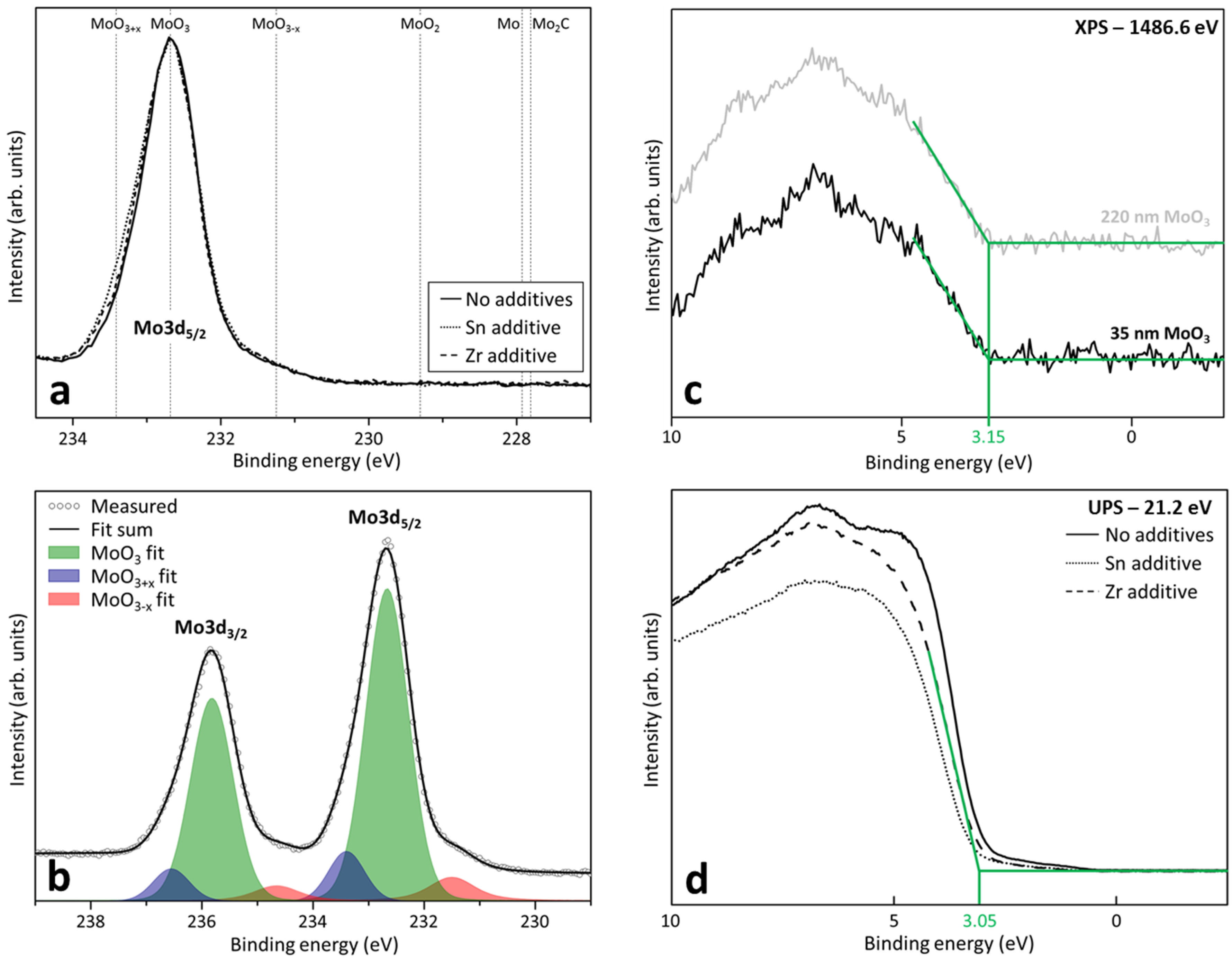
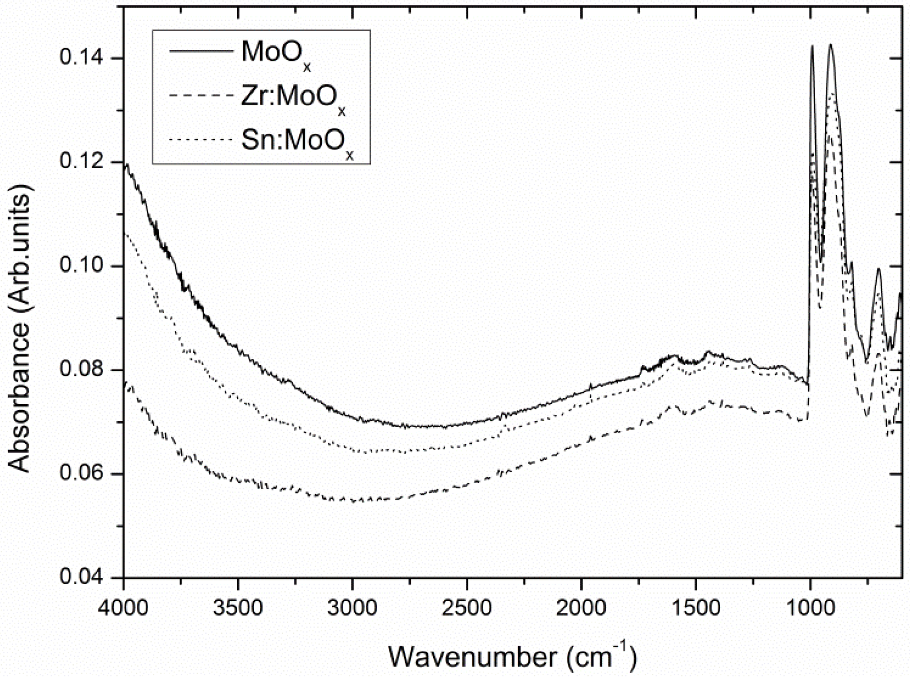
2.1. Composition and Electronic Structure

To investigate the influence of the presence of zirconium and tin inside MoOx HTLs in organic photovoltaics, Zr- and Sn-containing molybdenum oxide films were compared to unmodified MoOx films via complementary analysis techniques. Thermogravimetric analysis (TGA) results obtained on dried fine powders (grain size <63 µm) show a very similar decomposition process for all three precursor systems (Figure S2). Hence, all spin coated layers received an identical thermal treatment. The chemical structure of the unmodified Sn-containing and Zr-containing molybdenum oxide layer was evaluated by grazing incidence attenuated total reflection Fourier transform infrared spectroscopy (GATR-FTIR). Figure 1 shows the infrared spectra of spin-coated layers on ITO substrates. All films received an identical thermal treatment up to 300 °C. The small absorbance signals at 1445 cm−1, 1593 cm−1, and 1733 cm−1 indicate a minor residual organic fraction originating from the acetylacetonate salts used in the precursor system. However, the most distinct signals in all spectra can be appointed to characteristic Mo-O vibrations: 995 cm−1 (O-Mo stretch), 902 cm−1, and the shoulder at 822 cm−1 (both corresponding to a Mo-O-Mo stretch) can be identified. The shape of the bands strongly resembles the o-MoO3 spectrum reported by Seguin et al. [40]. The signal at 696 cm−1 is deviating from the reported values. This comes as no surprise, as the infrared spectra of MoO3 are known to be dependent on the morphology of the crystallites [40] and the so-called transverse optic and longitudinal optic (TO-LO) splittings [41]. This result suggests that the processed MoOx layers are very similar to stoichiometric MoO3, although the MoOx notation will be conserved throughout the article. Nonetheless, all spectra show strong similarities, suggesting that the additives have a negligible influence on the molybdenum oxide composition and chemical structure.
Based on cross-section SEM (Figure S3), the MoOx layer thickness is estimated to be approximately 35 nm, and is assumed to be similar for the modified layers. The surface composition of all layers has been investigated in more detail by means of X-ray photoelectron spectroscopy (XPS). It is remarkable that an indium signal can be observed in the survey scans. This can point to incomplete surface coverage (pores) which exposes the ITO surface underneath the (approx. 35 nm) MoOx films. Alternatively, indium diffusion through the MoOx layer during the heat treatment (up to 300 °C) is considered, albeit rather unlikely at the given experimental conditions [42,43]. The origin of the indium signal was critically addressed by growing a thicker MoOx film on top of the ITO substrate (eight deposition cycles instead of one, including eight temperature treatment cycles, Figure S4). As no indium signals were found at the surface of the thicker layer (which would be the case if diffusion occurred), the occurrence of pores is adopted as the reason for the observation of indium in the 35-nm thin MoOx HTLs. A certain degree of porosity was expected for deposition from combustion precursors, due to outgassing of the organic components during the formation of the oxide. Considering the roughness of the surface (vide infra), it was not possible to quantify the incidence of the pores by means of angular resolved XPS. In the case of the Sn-containing precursor, the presence of chlorine could possibly induce HCl formation, which etches the ITO electrode underneath the MoOx layer. HCl evolution could indeed be detected in TG-MS (thermogravimetric analysis - mass spectroscopy, Figure S4), but the quantity of evolved gas is very small, and no Cl are detected in the resulting layers, which excludes a doping effect influencing the n-type character of MoOx (Figure S5). Moreover, the presence of indium could also be detected in the Zr-modified and unmodified layers, deposited from precursors which do not consist of any chlorine species. Therefore, it can be stated that incomplete surface coverage is the main explanation for the observed presence of indium.
Furthermore, the presence of the added Sn and Zr species could be confirmed, as their corresponding signals could be identified in the XPS survey scans (Figure S5). For the Sn-containing MoOx layer, an increased tin/indium ratio compared to the expected typical 1/10 ratio for the bare underlying ITO substrate was observed, confirming the Sn presence in the MoOx HTL.
In literature, the formation of an oxide with mixed molybdenum oxidation states (Mo(V) and Mo(VI)) is identified as an important performance parameter that influences the OPV device results [18,26]. It affects the electronic structure of molybdenum oxide, and thereby the hole extraction efficiency, charge recombination at Mo(V) gap states, the series resistance [44], and the shunt resistance (in OPV) [26]. However, this work (Figure 2a) demonstrates a strong resemblance between the unmodified and Zr- or Sn-incorporated MoOx layers. In all cases, the molybdenum 3d5/2 core level is situated at the expected position for Mo(VI), being 232.7 eV, indicating the formation of mainly MoO3. Especially in the sub-stoichiometric MoO3-x region (towards lower binding energies, in which Mo occurs in the (V) or even (IV) oxidation state), the similarity between the Zr-containing, Sn-containing, and unmodified MoOx layer is remarkable (Figure 2b). Therefore, an eventual difference in device performance cannot be attributed to changes in the molybdenum oxidation state. The weak MoO3+x contribution—which can be recognized at the high binding energy side of the molybdenum 3d5/2 core level—points to the presence of a small fraction of Mo vacancies in unit cells which are in close proximity to the probed Mo atoms (thus resulting in a higher effective coordination with oxygen around the probed Mo atoms). This can be expected, as the formation of a perfect stoichiometric oxide material is unlikely at the low processing temperatures (300 °C). An alternative explanation could be charging in some regions due to the rather insulating properties of the investigated material (thus reflecting the volume fraction with perfect crystal structure). Hence, the molybdenum oxide layers will be continuously referred to as MoOx, as no perfect Mo/O = 1/3 ratio is achieved. Moreover, according to Figure 2a, the presence of Mo2C can be ruled out for all of our samples, thus excluding this phase as a potential reason for an enhanced conductivity (Mo2C has a reported electrical resistivity of 71 µΩ·cm [45]).
To investigate possible modifications in the electronic structure induced by Zr and Sn additives, measurements of the valence band structure exploiting x-ray photoelectron spectroscopy (XPS, Figure 2c) and ultraviolet photoelectron spectroscopy (UPS, Figure 2d) were conducted. From these figures, the position of the valence band maximum with respect to the Fermi energy (the latter corresponding to zero binding energy) can be extracted, resulting in values of 3.15 eV (XPS) and 3.05 eV (UPS), both agreeing fairly well with literature results reported for undoped MoO3 [46]. Consequently, by considering the band gap of MoO3, a n-type character for all samples can be extracted, as the Fermi level is pinned close to the conduction band minimum, independent of whether or not additives are present.
Moreover, the XPS measurement (Figure 2c) indicates a similar valence band maximum for the 35 nm-thick and the 220 nm-thick layers, providing supplementary proof that no indium diffusion takes place. Although slight changes in band structure can be noted if the UPS measurements (Figure 2d) for the different layers are carefully compared, the most plausible cause is surface contamination, as the UPS sampling depth is only 1 nm, and the samples were prepared ex-situ. As such, it can be confirmed that Sn and Zr will act as additives, rather than as dopants. Changes in the performance of OPV or OLED devices with Zr- or Sn-containing MoOx HTLs (discussed further) can therefore not be assigned to a change of the MoOx valence band minimum or the formation of intermediate levels in the band gap.

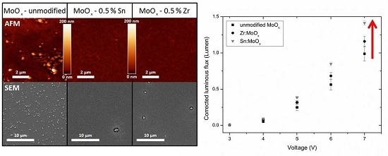
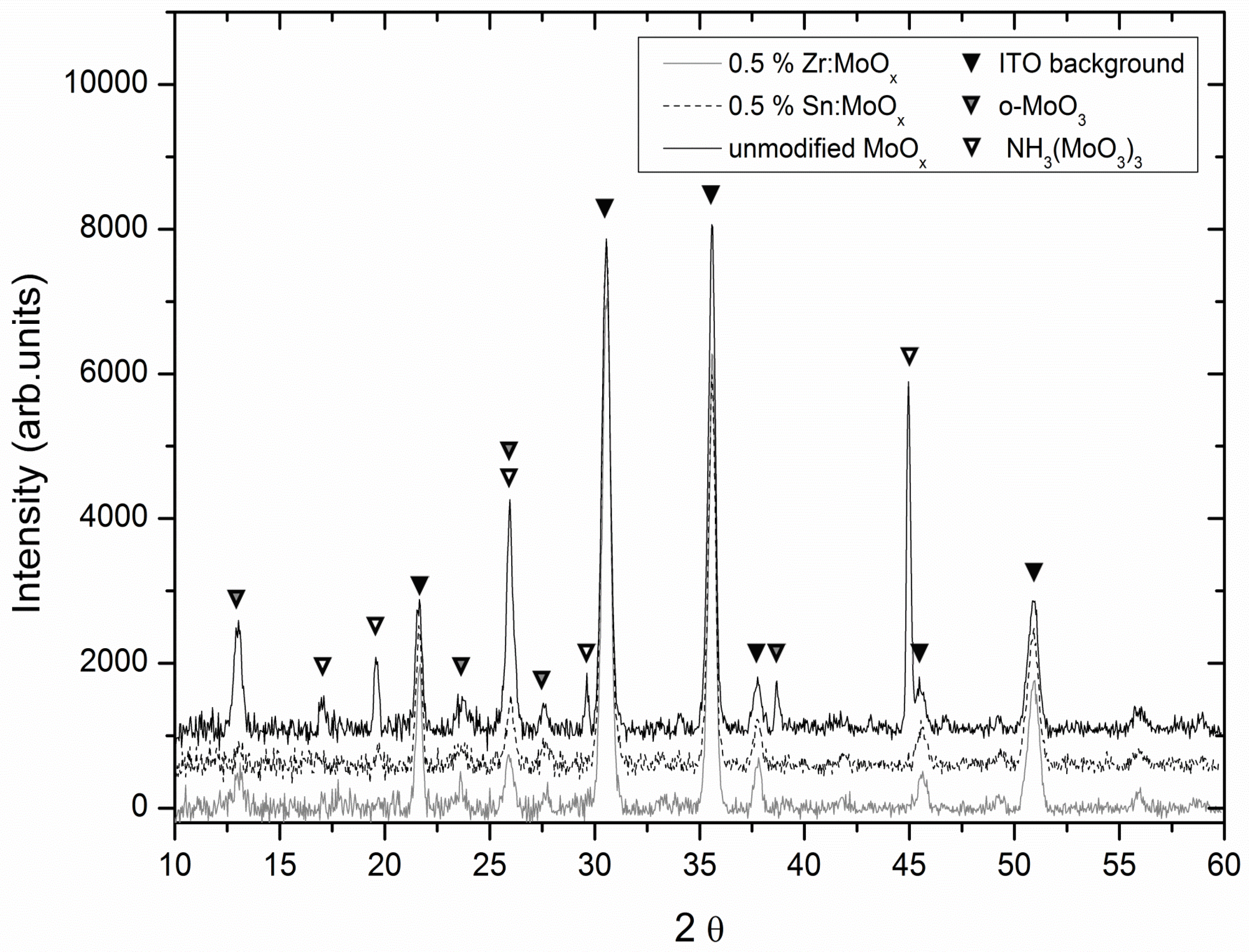
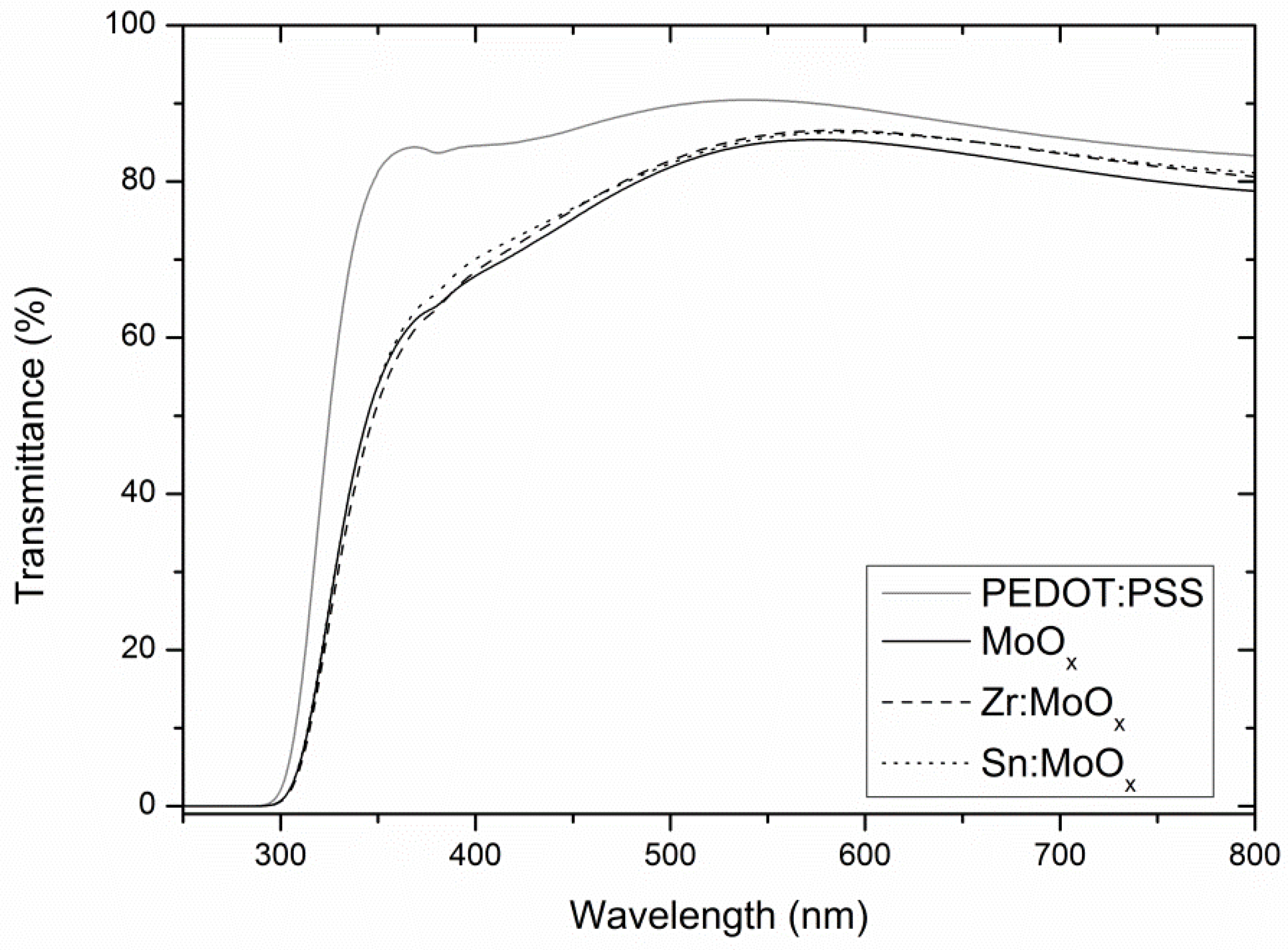
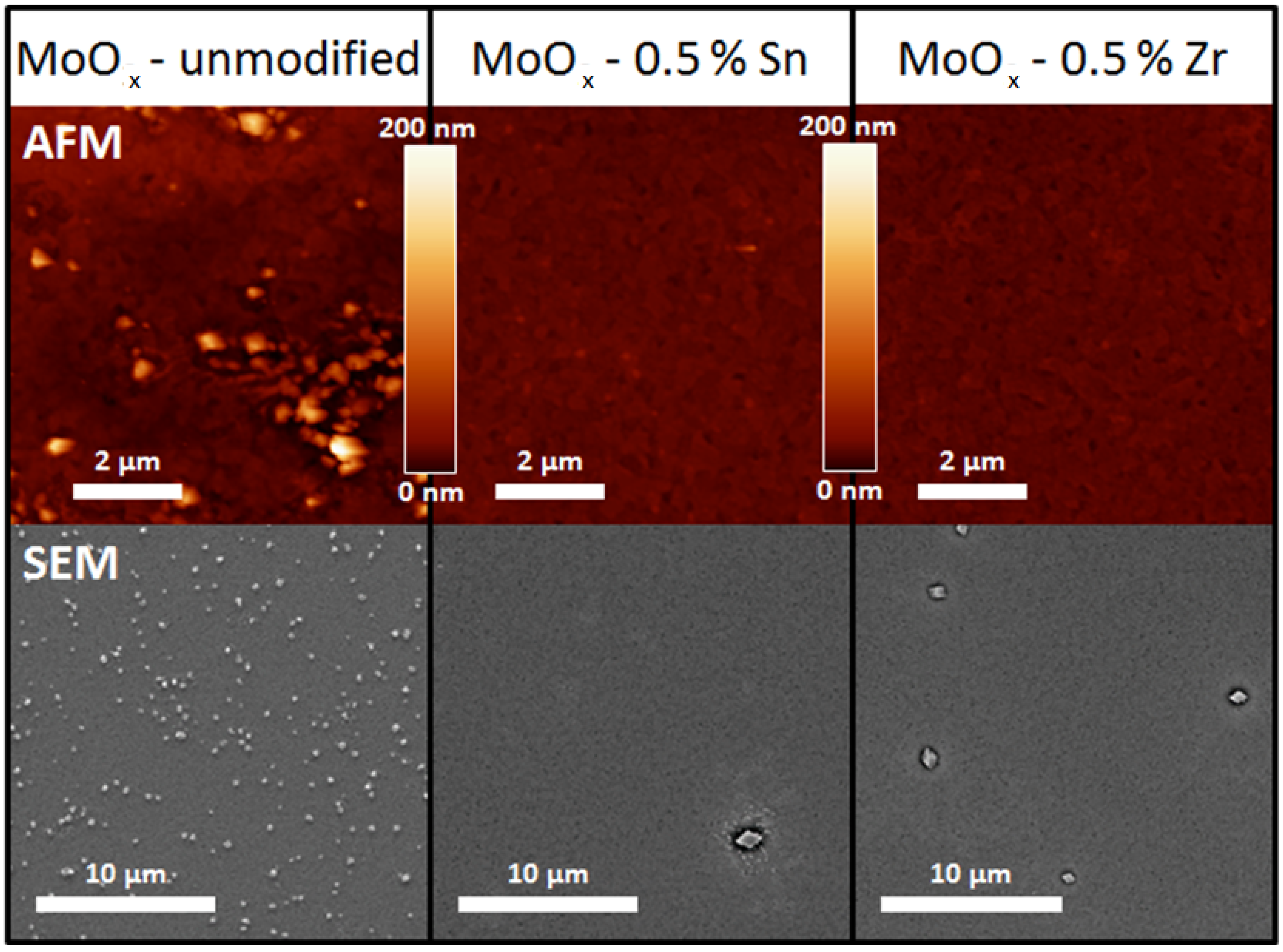
2.2. Morphology and Crystallinity

The morphology of the unmodified, Zr-containing, and Sn-containing layers was analyzed via atomic force microscopy (AFM) and scanning electron microscopy (SEM). In Table 1, the root mean square (RMS) roughness—measured by AFM—for the different MoOx-based layers is presented, together with the results for a PEDOT:PSS reference layer which is used in the OLED and OPV control devices (vide infra). The results were obtained on different identically-processed samples (nsamples). From Table 1, it becomes clear that the introduction of additives has a significant influence on the layers’ roughness. Whereas the unmodified MoOx layer exhibits an extremely high mean RMS roughness of approx. 19 nm (discussed further), the roughness reduces drastically upon the addition of zirconium and tin into the combustion precursor, down to below 3 nm. However, in this case, the presence of additives does not dramatically affect the outgassing during the precursor decomposition pathway (as illustrated by TGA, Figure S2). Both zirconium and tin are introduced in a very limited amount (0.5%) using similar acetylacetonate compounds, and no catalytic decomposition effect can be observed in the TGA profiles. In addition, it can be observed that the high doping flexibility inherent to the acetylacetonate chemistry (described in the introduction) comes with the cost of higher annealing temperatures compared to alternative routes [27,29]. Since the roughness of the additive-containing layers is comparable to the blank ITO RMS roughness (1.8 nm) and the PEDOT:PSS reference layer, these HTL layers show a lot of promise for subsequent deposition of the photoactive layer on top of it. In contrast, the unmodified MoOx layer exhibits an unfavorable topography, which is expected to negatively influence the performance due to structural (and interfacial) irregularities in the processed devices. Indeed, an RMS value of 18.8 nm corresponds to huge peak-to-peak values. The roughness of the unmodified layer even exceeds values reported for HTLs produced from nanoparticle suspensions [47].
The morphological changes are more clearly visualized by AFM and SEM. The most representative results are shown in Figure 3, and a complete presentation of the SEM images is provided in Figure S6. Detailed analysis of the images reveals the cause of the increased roughness for the unmodified MoOx samples compared to the Sn- or Zr-modified oxide layers. On the surface, a varying amount of small grains is visible. The surface density of these grains is much higher for the unmodified MoOx layer. On the Zr- and Sn-containing layers, however, the presence of the grains diminishes notably. Combining these observations with the AFM results in Table 1, it is evident that the presence of these grains gives rise to the increased RMS roughness. Thus, the addition of zirconium and tin additives to the molybdenum combustion precursor influences the morphology of the resulting layers in a beneficial way by reducing the occurrence of grains on the surface. Moreover, a zoomed in image of a crystallite-containing region is presented in Figure S7. Aside from the presence of crystallites, the image demonstrates that parts of the surface remain uncovered, accounting for the indium peaks observed in XPS.
X-ray diffraction (XRD) measurements were performed to investigate the nature of the grains, and the resulting diffractograms are shown in Figure 4. All analyzed films were deposited on ITO substrates, which were also measured separately to identify the background (Figure S8). The unmodified MoOx film clearly shows more intense peaks, corresponding to the orthorhombic MoO3 phase and the NH3(MoO3)3 phase [48]. The presence of the latter could be the result of a hampered outgassing of the NH3 from the thicker stack (four subsequent layers were deposited to improve diffractogram quality). This hindered outgassing can be postulated, as the diffractogram of a single layer treated at the same conditions (Figure S5) does not show this secondary phase (or it is below the detection limit). The presence of NH3 is specific for the employed synthesis route, as the combustion precursor contains a considerable amount of ammonium nitrate [31]. The peaks which belong to the underlying ITO remain similar for all samples, and the diffractograms were collected with the same acquisition time and parameters. It can be concluded that more crystalline material is present in the unmodified MoO3 film, since the molybdenum phase-specific peaks are much more intense. This can potentially be linked to the strong presence of small o-MoO3 crystallites on the MoOx surface. Hence, the amount of crystallites on the surface influences the RMS roughness, and most likely the performance of the functional devices in which they are included as HTL. In other words, the presence of both zirconium and tin influences the nucleation and growth kinetics of the surface grains, consequently reducing the roughness.
In addition, higher additive percentages were investigated to check whether the crystallization suppression effect would still hold. As demonstrated in Figure S9, a layer resulting from a 10% Zr-containing precursor barely exhibits any signs of o-MoO3 presence, although processing conditions were identical to the MoOx layers presented in the above diffractogram (also four subsequent depositions). However, a higher additive content had an unfavorable effect on the device performance, which led to the hypothesis that the addition of 0.5% is sufficient to reduce the layer roughness without introducing large amounts of ZrO2 into the HTL, probably causing a suboptimal band overlap given the high band gap of this oxide [49].
Finally, the transparency of the layers was evaluated by UV-Vis spectroscopy. As XPS results proved that the additives do not have a significant effect on the bandgap of the HTLs, only roughness-related effects (e.g., light scattering) can justify differences in the spectra. Moreover, phase segregation resulting in ZrO2 and SnO2 is not expected to affect the transmission, as both materials exhibit a large band gap and high transparency in the visible spectrum [15,50]. From Figure 5, it becomes clear that the solution-processed molybdenum oxide layers underperform compared to 35 nm PEDOT:PSS reference layers (HTL in traditional organic electronic devices) for this particular device stack. The spin coating of a PEDOT:PSS layer with comparable thickness was achieved via an optimization as a function of spin speed, whereupon the thickness was determined via profilometry (Figure S10). Differences between the unmodified and Zr- or Sn-containing molybdenum oxide layers are miniscule: a maximum effect can be noticed in the high wavelength range of the UV-Vis scan.
At 800 nm, the Zr- and Sn-containing layers have an average transparency of 80.6% ± 1.7% and 81.1% ± 0.9%, respectively, compared to an average transparency of 78.8% ± 2.3% for the unmodified layer. However, these differences are situated within the estimated standard deviation (calculated at 800 nm), so no significant change can be reported. The fact that no significant difference could be observed means that the eventual (Mie–Lorentz) light scattering by the MoOx surface grains affects the general optical properties to a very limited extent. The conversion to Tauc plots is not reported, as the band gaps were previously determined via XPS and UPS. The transparency of PEDOT:PSS at 800 nm is 83.0% ± 0.1%, and its performance with respect to the processed MoOx layers increased towards decreasing wavelengths, which can partially explain its superior performance in the processed OPV and OLED devices (vide infra).
So far, the study showed that the addition of Zr and Sn heteroatoms to the molybdenum oxide layer does not result in the formation of an alternative crystallographic phase, and the molybdenum valencies remain unaffected, excluding the formation of performance-enhancing defects or a better alignment in the electronic band structure. On the other hand, the smoother morphology of the Zr- and Sn-containing layers might have an effect on the OPV and OLED parameters when employed as the HTL prior to active layer deposition. The potential changes in device output are not related to variations in transparency, as illustrated above, which is an important parameter to exclude from the OLED and OPV output analysis in the following section.

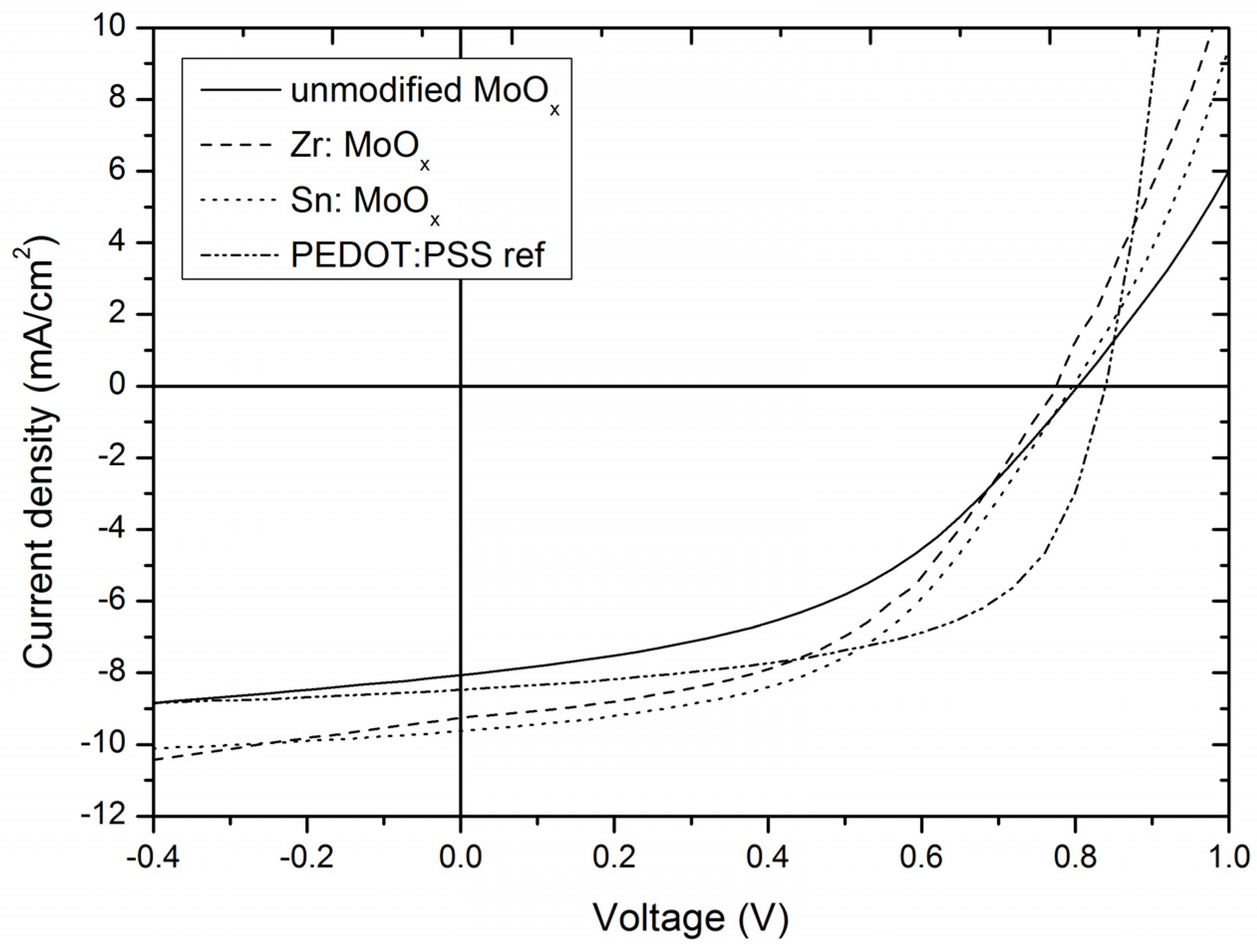
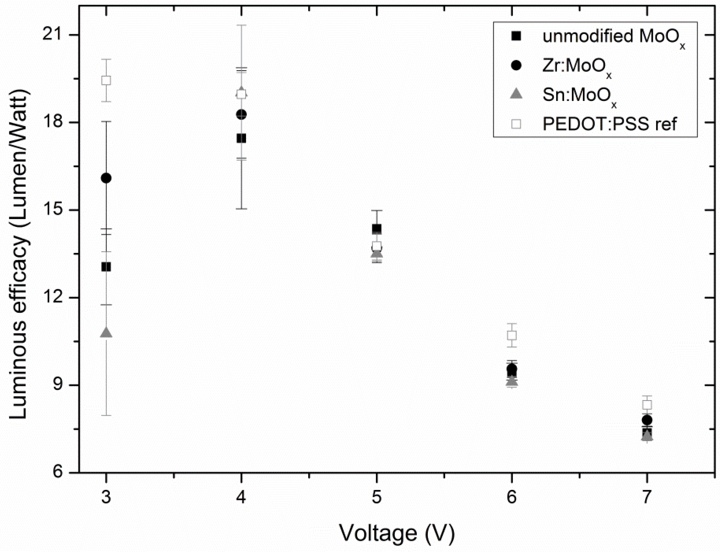
2.3. Device Output Characteristics

The performance of OPVs containing the unmodified MoOx layer were compared to devices with Zr- and Sn-containing HTLs. From the results presented in Table 2 and Figure 6, it can be concluded that the introduction of both zirconium and especially tin leads to an increased average power conversion efficiency (PCE). As 28 device tests were performed to assess the PCE average and standard deviation of the unmodified MoOx-containing devices, the Sn-modified layers can especially be considered as significant improvements (P = 0.96, y0 = 3.62, η = 3.10, according to Student t distribution with s = 0.28 and 27 degrees of freedom). The gain in efficiency can mainly be attributed to the unmistakable increase in the short-circuit current density for the devices containing the modified HTLs. It can be hypothesized that the reason for this ameliorated current density is the observed change in morphology: as the molybdenum oxide HTL is first in the deposition sequence, its unfavorable topography is likely to affect the overlying layers (including the active layer). In case of the Sn and Zr modified layers, the active layer can be deposited on a smoother surface, preventing void formation. Moreover, Novikov [51] calculated that increased roughness of the inorganic–organic interface results in an inhomogeneous distribution of the electric field, reducing the efficiency and stability of the resulting device. Eventually, the presence of the crystallites on the unmodified MoOx surface can lead to a sub-optimal contact between the HTL and the photoactive layer, decreasing the output characteristics (and more specifically Jsc). A similar effect was observed by Qin et al., as they reported a decrease in efficiency and short-circuit current density due to the suboptimal roughness of the ZnO electron transporting layer in an OPV with inverted architecture [52]. In this study, a decrease in output characteristics was observed from the moment the RMS roughness of the interface layer exceeded 7 nm, which is also the case for the unmodified MoOx HTL. This can be rationalized by the decreasing contact area (void formation) between the interface and the active material, impeding the charge transport to the electrodes. Further evidence for the correlation between the device performance and the MoOx interface problem could be observed in the dark J–V curves (Figure S11). The higher leakage current for the unmodified MoOx compared to the additive-containing layers is remarkable. The lower shunt resistance (Rsh) in the unmodified MoOx-containing layers is plausibly caused by the many crystallites observed on the MoOx surface. Furthermore, the leakage current and Rsh follow the same trend as the extracted RMS roughness values (Table 1). The PCE difference between the Zr- and Sn-modified MoOx-containing devices could not be explained based on the performed dark J–V measurements.
Finally, a reference cell using a PEDOT:PSS interface layer is presented in Figure 6 and Figure S11. Although the modified MoOx layers obtain similar short circuit current densities, the fill factor is still superior, resulting in average PCE values of 4.11% (12 device average). The superior fill factor can be rationalized considering the higher Rsh and lower Rs, as shown in Figure S11. Moreover, the PEDOT:PSS-containing device exhibits a lower leakage current. Further optimization regarding the morphology, HTL thickness, and the MoOx stoichiometry are still necessary to bridge this gap [53], although the reported device efficiencies incorporating solution-processed MoOx are state-of-the-art [20,26]. In spite of the lower initial PCE of the (modified) MoOx-containing devices compared to PEDOT:PSS, a prolonged stability and long-term performance can be expected based on multiple studies [54,55]. Moreover, the main target of this paper is to link the interface engineering of the MoOx layers to their resulting performance and to stress the transferability of these findings to other oxide interface layers, such as the ZnO electron transporting layers mentioned above.
If the decrease in current density for unmodified MoOx layers is ascribed to a morphology-related problem induced by the high abundancy of small crystallites on the surface, the same trend of decreasing performance should also be present in other functional devices in which MoOx fulfills a similar function. Therefore, OLEDs were processed via deposition of (modified) MoOx layers on ITO substrates, from which the rest of the stack was build up. Figure 7 shows the average luminous flux for the best batch of processed OLEDs. Although batches with inferior absolute luminous flux results were produced (Figure S12), the following trends could always be observed: devices which include the Sn-modified HTL always perform slightly better than the Zr-containing variation and significantly better compared to the unmodified MoOx. The differences in luminous flux are very obvious at higher voltages (6–7 V). This increased performance cannot be ascribed to a change in light absorption by the HTL, as Figure 5 showed a resembling transparency for all the investigated HTLs. Moreover, Figure 8 shows the differences in luminous efficacy for all processed OLED samples, demonstrating no obvious trend among modified and unmodified layers (with considerable variance at low voltages, depicted by the error bars), obtaining maximum efficacies at 4 V. At higher voltages (6–7 V), the luminous efficacies of all different HTLs seem to converge into a singular value. The fact that the best flux results could be achieved with the Sn-containing layers and no corresponding clear increase in efficacy could be observed (in fact, the efficacies at high voltages are more or less equal, whereas the luminous flux is clearly better for additive containing samples) implies that more current is running through the devices containing the modified HTL. The current densities for the investigated (modified) MoOx HTL-containing OLEDs are demonstrated in Figure S12, confirming the aforementioned explanation. This further strengthens the conclusion drawn from the OPV results (increase in Jsc due to interface improvements), and confirms the improved hole transport through the modified MoOx layers due to the hypothesized ameliorated interface contact. Similar to the OPV test, PEDOT:PSS also proves to still be a better-performing interface layer, as its corrected luminous flux is higher compared to all the MoOx layers. However, the incorporation of Zr and especially Sn results again in a remarkable improvement. The emission spectra of all processed OLEDs are similar, and a maximum intensity could be observed around a wavelength of 550 nm (see Figure S14).

3. Materials and Methods

3.1. Precursor Synthesis

Precursor synthesis was based on previously reported procedures involving the preparation of a combustion precursor [31]. Molybdenyl(VI)acetylacetonate, (MoO2(acac)2, 99% Alfa Aesar, Karlsruhe, Germany) and ammonium nitrate (extra pure >98.5%, Merck, Darmstadt, Germany) were dissolved in methanol (>99.9% Acros Organics, Geel, Belgium) in a 1:2 molar ratio to obtain a 0.2 M molybdenum concentration. This stock solution was diluted to 0.1 M with methanol in the case of the pure MoOx precursor. From now on, we will refer to the unmodified MoOx precursor in case no other metal salts are added. The introduction of zirconium and tin was achieved by dissolving 0.01 M of zirconium(IV)acetylacetonate (98%, Fluka Chemika, Buchs, Switzerland) and tin(IV)bisacetylacetonate dichloride (98%, Sigma-Aldrich, Steinheim, Germany), respectively, in methanol. Subsequently, the appropriate amount of zirconium- or tin-containing precursor was added to the 0.2 M molybdenum precursor to obtain a final ratio of 0.5% (expressed as [Zr]/[Mo] or [Sn]/[Mo] in both multi-metal precursors, so as a molar percentage), and pure methanol was added to reach a 0.1 M molybdenum concentration, similar to the unmodified MoOx precursor.

3.2. Film Deposition

MoOx films and their Zr- and Sn-containing variants were obtained by spin coating (3000 rpm, 30 s, 1000 rpm·s−1) the freshly prepared precursor on ITO-coated glass substrates (Kintech, 100 nm, 20 Ohm·sq−1). The underlying ITO layer was soft-cleaned prior to deposition (sonication in water/acetone/2-propanol for 10 min each, followed by a 30 min UV-O3 treatment at 60 °C). The deposited layers were thermally treated in ambient conditions on a hotplate for 2 min at 80 °C and 200 °C to dry and decompose the precursor, whereupon a final annealing step at 300 °C (2 h in 1000 mL/min dry air) was applied using rapid thermal processing (RTP, Annealsys, AS-one) to remove residual organics. For all analysis techniques and devices, only a single MoOx layer was deposited via this procedure, except for the samples characterized by X-ray diffraction (XRD) and in case of the indium diffusion investigation via XPS. In these cases, four layers and eight layers (approx. 220 nm thickness) were spin-coated, respectively, and heated until 200 °C, after which the final temperature step of 300 °C in the RTP was performed. This resulted in a thicker layer to improve the quality (signal–noise ratio) of the diffractograms. An XRD pattern of single-layered MoOx was added to the supporting information (Figure S1) for comparison. Films resulting from the unmodified MoOx precursor will be referred to as unmodified MoOx layers in the following, whereas films containing the Sn and Zr heteroatoms are addressed as modified or Zr- and Sn-containing MoOx layers.

3.3. Film Characterization

The spin coated and decomposed MoOx HTLs were characterized by performing grazing incidence attenuated total reflection Fourier transform infrared (GATR-FTIR) measurements on a Bruker Vertex 70 spectrometer, by means of a 65° single reflection Ge-ATR unit in the sample compartment (4000–600 cm−1, 36 scans, spectral resolution 4 cm−1, torque 56 ounce·inch−1). X-ray photoelectron spectroscopy measurements were performed on a Physical Electronics (PHI) 5600 LS photoelectron spectrometer. Core-level spectra were acquired using monochromatic Al Kα X-rays (1486.6 eV), with a beam spot size of about 1 mm2. The binding energy scale was calibrated using an independent Au reference sample, fixing the Au 4f7/2 core level position to 84.00 eV. The morphology of the deposited layers was studied via atomic force microscopy (AFM, Bruker, multi-mode 8 microscope, JVLR-piezo) with a Bruker Sb-doped Si Tap525A tip with a spring constant k of 200 N/m in tapping mode to extract the root mean square (RMS) roughness. Average RMS roughness results of multiple measurements (32 in total, collected on 12 different samples; 4 out of 32 were considered as outliers) are reported, using the WSxM software package [56]. Scanning electron microscopy (SEM) images were obtained using an FEI Quanta 200 FEG-SEM equipped with secondary- and back-scattered electron detectors. X-ray diffraction measurements were recorded by a Brüker D8 diffractometer with Cu-Kα radiation (room temperature, 0.04° steps, 3 s per step, LynxEye detector, 2θ range: 10–60°). The transparency of the different layers was evaluated by UV-Vis spectroscopy (Cary UV-Vis-NIR spectrometer, Agilent Technologies, scan mode, 10 nm/s scan rate) in which the coated ITO substrates could be fixed in a dedicated sample holder. Only the air background was subtracted, resulting in transparency scans including the ITO and glass substrate light absorption.

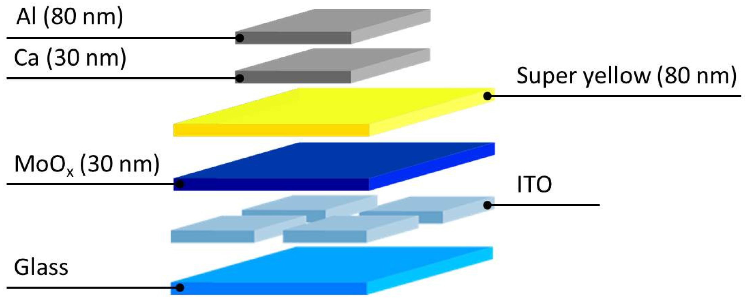
3.4. Device Processing

Organic light emitting diodes (OLEDs) were processed by coating patterned ITO substrates (Kintech, 100 nm, 20 Ohm·sq−1) with the molybdenum precursor, as described in the film deposition section. The PPV-polymer Super Yellow (PDY-132 from Merck) was dissolved in chlorobenzene with a mass concentration of 5 mg/mL and stirred overnight at a temperature of 50 °C in an inert atmosphere glove box system (O2/H2O ppm <0.1). The solution was cooled down to room temperature and spin-coated on top of the MoOx layer to obtain an emissive layer of 80 nm. Subsequently, the top electrodes—calcium (30 nm) and aluminum (80 nm)—were thermally evaporated at a base pressure of 10−7 mbar. The complete device stack is presented in Figure 9.
The produced OLEDs were measured using a Keithley 2401 source meter to obtain the current and voltage characteristics and by using an absolute calibrated integrating sphere spectrometer from Avantes to acquire the luminous flux. The luminous efficacy was then calculated out of the obtained data, dividing the luminous flux by the power.
Bulk heterojunction (BHJ) organic solar cells were fabricated utilizing a similar device architecture as for the OLEDs, apart from the exchange of the emissive layer by a photoactive layer, comprised of a PCDTBT:PC70BM (poly[[9-(1-octylnonyl)-9H-carbazole-2,7-diyl]-2,5-thiophenediyl-2,1,3-benzothiadiazole-4,7-diyl-2,5-thiophenediyl]:[6,6]-phenyl-C70-butyric acid methyl ester) donor–acceptor copolymer blend. This implies an ITO layer thickness of 100 nm, and a 30 nm Ca/80 nm Al layer as the top electrode (Figure S15). The (modified) molybdenum oxide layer-coated substrate was transferred to an inert atmosphere (glovebox) for spin-coating of the active layer using a solution containing 4 mg/mL PCDTBT (poly[[9-(1-octylnonyl)-9H-carbazole-2,7-diyl]-2,5-thiophenediyl-2,1,3-benzothiadiazole-4,7-diyl-2,5-thiophenediyl]; Solarischem) and 16 mg/mL PC70BM ([6,6]-phenyl-C70-butyric acid methyl ester; Solenne), dissolved overnight in ortho-dichlorobenzene (Sigma Aldrich). As such, a layer thickness of 60–80 nm was obtained. The OPV output characteristics were determined using a Newport class A (model 91195A) solar simulator, calibrated with a silicon solar cell, producing an AM 1.5 G spectrum.

4. Conclusions

Zirconium- and tin-containing MoOx layers were deposited via combustion solution processing, and both their composition and morphology were evaluated. As the unmodified, Zr-containing, and Sn-containing HTLs only differ in morphology due to a varying surface concentration of crystalline grains, the improved performance of OLEDs and OPVs incorporating the additive containing layers can be ascribed to the observed morphological differences. Therefore, the Sn and Zr species are referred to as additives instead of dopants. No proof of incorporation into the MoOx phase and related changes in the electronic band structure could be observed. The reported morphological interface optimization has a plausible transferability to other interface layers used in photovoltaic devices. The hole transport is expected to improve in devices processed with additive containing HTLs because of the enhanced contact between the smooth, modified MoOx layer and the active material. This effect is observed both in the short-circuit current density and the luminous flux for OPVs and OLEDs, respectively. Thus, the study illustrates the major importance of the morphology of interface layers which is a relevant factor to consider for all research on the optimization of organic electronics optimization.

Supplementary Materials

The following are available online at https://www.mdpi.com/1996-1944/10/2/123/s1. The supporting information includes 15 figures, labeled from S1 to S15, presented in a 10 page document.

Acknowledgments

The work was supported by the FWO, The research Foundation of Flanders [project G041913N]. The author would also like to acknowledge Ilaria Cardinaletti and Jeroen Drijkoningen for the AFM support and Huguette Penxten for the assistance concerning the UV-Vis measurements.

Author Contributions

Wouter Marchal: first author of the article. Inge Verboven: important contribution regarding the processing and characterization of OLEDS. Jurgen Kesters: Imprortant contribution regarding the processing and characterization of OPVs and corrected the manuscript. Boaz Moeremans: performed XPS measurements and was editing and optimizing the figures in the publication. Christopher De Dobbelaere: performed FTIR-GATR and AFM measurements which are discussed in the article and corrected the manuscript. Gilles Bonneux: performed SEM measurements which are discussed in the article and corrected the manuscript. Ken Elen: performed XRD measurements which are discussed in the article. Bert Conings: contributed by optimizing the UPS set-up and investigated MoO3 containing perovskite solar cells (not included in this publication). Wouter Maes: took part in the discussion involving the OPVs and corrected the manuscript. Hans-Gerd Boyen: made an important contribution to the XPS and UPS section of the manuscript. Wim Deferme: took part in the discussion involving the OLEDs and corrected the manuscript. Marlies Van Bael: performed multiple revisions of the manuscript and enabled the research by guiding the first author (as a promotor). An Hardy: performed multiple revisions of the manuscript, suggested and co-designed the experiments (as a promotor), provided funding for the work.

Conflicts of Interest

The authors declare no conflict of interest.

References

  1. Youn, H.; Park, H.J.; Guo, L.J. Organic photovoltaic cells: From performance improvement to manufacturing processes. Small 2015, 11, 2228–2246. [Google Scholar] [CrossRef] [PubMed]
  2. Fujita, S. Wide-bandgap semiconductor materials: For their full bloom. Jpn. J. Appl. Phys. 2015, 54, 030101. [Google Scholar] [CrossRef]
  3. Alivov, Y.I.; Kalinina, E.V.; Cherenkov, A.E.; Look, D.C.; Ataev, B.M.; Omaev, A.K.; Chukichev, M.V.; Bagnall, D.M. Fabrication and characterization of n-ZnO/p-AlGaN heterojunction light-emitting diodes on 6h-sic substrates. Appl. Phys. Lett. 2003, 83, 4719. [Google Scholar] [CrossRef]
  4. Thejokalyani, N.; Dhoble, S.J. Novel approaches for energy efficient solid state lighting by RGB organic light emitting diodes—A review. Renew. Sustain. Energy Rev. 2014, 32, 448–467. [Google Scholar] [CrossRef]
  5. Zhan, X.; Zhu, D. Conjugated polymers for high-efficiency organic photovoltaics. Polym. Chem. 2010, 1, 409–419. [Google Scholar] [CrossRef]
  6. Suzuki, Y.; Zhang, Q.; Adachi, C. A solution-processable host material of 1,3-bis{3-[3-(9-carbazolyl)phenyl]-9-carbazolyl}benzene and its application in organic light-emitting diodes employing thermally activated delayed fluorescence. J. Mater. Chem. C 2015, 3, 1700–1706. [Google Scholar] [CrossRef]
  7. Yu, J.; Zheng, Y.; Huang, J. Towards high performance organic photovoltaic cells: A review of recent development in organic photovoltaics. Polymers 2014, 6, 2473–2509. [Google Scholar] [CrossRef]
  8. Ray, B.; Alam, M.A. Random vs regularized opv: Limits of performance gain of organic bulk heterojunction solar cells by morphology engineering. Sol. Energy Mater. Sol. Cells 2012, 99, 204–212. [Google Scholar] [CrossRef]
  9. Gilissen, K.; Stryckers, J.; Verstappen, P.; Drijkoningen, J.; Heintges, G.H.L.; Lutsen, L.; Manca, J.; Maes, W.; Deferme, W. Ultrasonic spray coating as deposition technique for the light-emitting layer in polymer leds. Org. Electron. 2015, 20, 31–35. [Google Scholar] [CrossRef]
  10. Eggenhuisen, T.M.; Galagan, Y.; Coenen, E.W.C.; Voorthuijzen, W.P.; Slaats, M.W.L.; Kommeren, S.A.; Shanmuganam, S.; Coenen, M.J.J.; Andriessen, R.; Groen, W.A. Digital fabrication of organic solar cells by inkjet printing using non-halogenated solvents. Sol. Energy Mater. Sol. Cells 2015, 134, 364–372. [Google Scholar] [CrossRef]
  11. Meyer, J.; Hamwi, S.; Kroger, M.; Kowalsky, W.; Riedl, T.; Kahn, A. Transition metal oxides for organic electronics: Energetics, device physics and applications. Adv. Mater. 2012, 24, 5408–5427. [Google Scholar] [CrossRef] [PubMed]
  12. Zhang, H.; Fu, Q.; Zeng, W.; Ma, D. High-efficiency fluorescent organic light-emitting diodes with MoO3 and PEDOT: PSS composition film as a hole injection layer. J. Mater. Chem. C 2014, 2, 9620–9624. [Google Scholar] [CrossRef]
  13. Salim, T.; Yin, Z.; Sun, S.; Huang, X.; Zhang, H.; Lam, Y.M. Solution-processed nanocrystalline TiO2 buffer layer used for improving the performance of organic photovoltaics. ACS Appl. Mater. Interfaces 2011, 3, 1063–1067. [Google Scholar] [CrossRef] [PubMed]
  14. Tokmoldin, N.; Griffiths, N.; Bradley, D.D.C.; Haque, S.A. A hybrid inorganic-organic semiconductor light-emitting diode using ZrO2 as an electron-injection layer. Adv. Mater. 2009, 21, 3475–3478. [Google Scholar] [CrossRef]
  15. Wang, Z.; Nayak, P.K.; Caraveo-Frescas, J.A.; Alshareef, H.N. Recent developments in p-type oxide semiconductor materials and devices. Adv. Mater. 2016, 28, 3831–3892. [Google Scholar] [CrossRef] [PubMed]
  16. Murase, S.; Yang, Y. Solution processed MoO3 interfacial layer for organic photovoltaics prepared by a facile synthesis method. Adv. Mater. 2012, 24, 2459–2462. [Google Scholar] [CrossRef] [PubMed]
  17. Jiang, K.; Zakutayev, A.; Stowers, J.; Anderson, M.D.; Tate, J.; McIntyre, D.H.; Johnson, D.C.; Keszler, D.A. Low-temperature, solution processing of TiO2 thin films and fabrication of multilayer dielectric optical elements. Solid State Sci. 2009, 11, 1692–1699. [Google Scholar] [CrossRef]
  18. Hammond, S.R.; Meyer, J.; Widjonarko, N.E.; Ndione, P.F.; Sigdel, A.K.; Garcia, A.; Miedaner, A.; Lloyd, M.T.; Kahn, A.; Ginley, D.S.; et al. Low-temperature, solution-processed molybdenum oxide hole-collection layer for organic photovoltaics. J. Mater. Chem. 2012, 22, 3249–3254. [Google Scholar] [CrossRef]
  19. Jasieniak, J.J.; Seifter, J.; Jo, J.; Mates, T.; Heeger, A.J. A solution-processed MoOx anode interlayer for use within organic photovoltaic devices. Adv. Funct. Mater. 2012, 22, 2594–2605. [Google Scholar] [CrossRef]
  20. Liu, J.; Wu, X.; Chen, S.; Shi, X.; Wang, J.; Huang, S.; Guo, X.; He, G. Low-temperature MoO3 film from a facile synthetic route for an efficient anode interfacial layer in organic optoelectronic devices. J. Mater. Chem. C 2014, 2, 158–163. [Google Scholar] [CrossRef]
  21. Zilberberg, K.; Trost, S.; Meyer, J.; Kahn, A.; Behrendt, A.; Lützenkirchen-Hecht, D.; Frahm, R.; Riedl, T. Inverted organic solar cells with sol-gel processed high work-function vanadium oxide hole-extraction layers. Adv. Funct. Mater. 2011, 21, 4776–4783. [Google Scholar] [CrossRef]
  22. Choi, H.; Kim, B.; Ko, M.J.; Lee, D.K.; Kim, H.S.H.; Kim, K. Solution processed WO3 layer for the replacement of PEDOT:PSS layer in organic photovoltaic cells. Org. Electron. 2012, 13, 959–968. [Google Scholar] [CrossRef]
  23. Vasilopoulou, M.; Soultati, A.; Georgiadou, D.G.; Stergiopoulos, T.; Palilis, L.C.; Kennou, S.; Stathopoulos, N.A.; Davazoglou, D.; Argitis, P. Hydrogenated under-stoichiometric tungsten oxide anode interlayers for efficient and stable organic photovoltaics. J. Mater. Chem. A 2014, 2, 1738–1749. [Google Scholar] [CrossRef]
  24. Girotto, C.; Voroshazi, E.; Cheyns, D.; Heremans, P.; Rand, B.P. Solution-processed MoO3 thin films as a hole-injection layer for organic solar cells. ACS Appl. Mater. Interfaces 2011, 3, 3244–3247. [Google Scholar] [CrossRef] [PubMed]
  25. Ma, J.W.; Liang, Z.; Jin, C.; Jiang, X.Y.; Zhang, Z.L. Enhanced power efficiency for white oled with MoO3 as hole injection layer and optimized charge balance. Solid State Commun. 2009, 149, 214–217. [Google Scholar] [CrossRef]
  26. Griffin, J.; Watters, D.C.; Yi, H.; Iraqi, A.; Lidzey, D.; Buckley, A.R. The influence of mooxanode stoicheometry on the performance of bulk heterojunction polymer solar cells. Adv. Energy Mater. 2013, 3, 903–908. [Google Scholar] [CrossRef]
  27. Choy, W.C.; Zhang, D. Solution-processed metal oxides as efficient carrier transport layers for organic photovoltaics. Small 2016, 12, 416–431. [Google Scholar] [CrossRef] [PubMed]
  28. Liu, F.; Shao, S.; Guo, X.; Zhao, Y.; Xie, Z. Efficient polymer photovoltaic cells using solution-processed MoO3 as anode buffer layer. Sol. Energy Mater. Sol. Cells 2010, 94, 842–845. [Google Scholar] [CrossRef]
  29. Xie, F.; Choy, W.C.; Wang, C.; Li, X.; Zhang, S.; Hou, J. Low-temperature solution-processed hydrogen molybdenum and vanadium bronzes for an efficient hole-transport layer in organic electronics. Adv. Mater. 2013, 25, 2051–2055. [Google Scholar] [CrossRef] [PubMed]
  30. Tan, Z.a.; Qian, D.; Zhang, W.; Li, L.; Ding, Y.; Xu, Q.; Wang, F.; Li, Y. Efficient and stable polymer solar cells with solution-processed molybdenum oxide interfacial layer. J. Mater. Chem. A 2013, 1, 657–664. [Google Scholar] [CrossRef]
  31. Marchal, W.; De Dobbelaere, C.; Kesters, J.; Bonneux, G.; Vandenbergh, J.; Damm, H.; Junkers, T.; Maes, W.; D’Haen, J.; Van Bael, M.K.; et al. Combustion deposition of MoO3 films: From fundamentals to opv applications. RSC Adv. 2015, 5, 91349–91362. [Google Scholar] [CrossRef]
  32. Li, X.; Choy, W.C.H.; Xie, F.; Zhang, S.; Hou, J. Room-temperature solution-processed molybdenum oxide as a hole transport layer with ag nanoparticles for highly efficient inverted organic solar cells. J. Mater. Chem. A 2013, 1, 6614–6621. [Google Scholar] [CrossRef] [Green Version]
  33. Gershon, T. Metal oxide applications in organic-based photovoltaics. Mater. Sci. Technol. 2011, 27, 1357–1371. [Google Scholar]
  34. Boukhachem, A.; Kamoun, O.; Mrabet, C.; Mannai, C.; Zouaghi, N.; Yumak, A.; Boubaker, K.; Amlouk, M. Structural, optical, vibrational and photoluminescence studies of Sn-doped MoO3 sprayed thin films. Mater. Res. Bull. 2015, 72, 252–263. [Google Scholar] [CrossRef]
  35. Kim, P.L.; Yusoff, A.R.M.; Kim, H.M.; Lee, H.J.; Seo, G.J.; Jang, J. Inverted organic photovoltaic device with a new electron transport layer. Nanoscale Res. Lett. 2014, 9, 1–9. [Google Scholar] [CrossRef] [PubMed]
  36. Chen, H.-Y.; Su, H.-C.; Chen, C.-H.; Liu, K.-L.; Tsai, C.-M.; Yen, S.-J.; Yew, T.-R. Indium-doped molybdenum oxide as a new p-type transparent conductive oxide. J. Mater. Chem. 2011, 21, 5745–5752. [Google Scholar] [CrossRef]
  37. Li, X.; Xie, F.; Zhang, S.; Hou, J.; Choy, W.C.H. Over 1.1 ev workfunction tuning of cesium intercalated metal oxides for functioning as both electron and hole transport layers in organic optoelectronic devices. Adv. Funct. Mater. 2014, 24, 7348–7356. [Google Scholar] [CrossRef]
  38. Li, X.; Xie, F.; Zhang, S.; Hou, J.; Choy, W.C.H. MoOx and V2Ox as hole and electron transport layers through functionalized intercalation in normal and inverted organic optoelectronic devices. Light Sci. Appl. 2015, 4, e273. [Google Scholar] [CrossRef] [Green Version]
  39. Moon, B.S.; Lee, S.-H.; Huh, Y.H.; Park, B. Hole-selective and impedance characteristics of an aqueous solution-processable MoO3 layer for solution-processable organic semiconducting devices. J. Korean. Phys. Soc. 2015, 66, 635–645. [Google Scholar] [CrossRef]
  40. Seguin, L.; Figlarz, M.; Cavagnat, R.; Lassègues, J.-C. Infrared and raman spectra of MoO3 molybdenum trioxides and MoO3.XH2O molybdenum trioxide hydrates. Spectrochim. Acta A 1995, 51, 1323–1344. [Google Scholar] [CrossRef]
  41. Eda, K. Longitudinal-transverse splitting effects in ir absorption spectra of MoO3. J. Solid State Chem. 1991, 95, 64–73. [Google Scholar] [CrossRef]
  42. Wang, Q.; Sun, J.; Wang, Q.; Zhang, D.-A.; Xing, L.; Xue, X. Electrochemical performance of α-MoO3–In2O3 core–shell nanorods as anode materials for lithium-ion batteries. J. Mater. Chem. A 2015, 3, 5083–5091. [Google Scholar] [CrossRef]
  43. Chang, J.H.; Liu, S.Y.; Wu, I.W.; Chen, T.C.; Liu, C.W.; Wu, C.I. Stability improvement of organic light emitting diodes by the insertion of hole injection materials on the indium tin oxide substrate. J. Appl. Phys. 2014, 115, 1–5. [Google Scholar] [CrossRef]
  44. Dasgupta, B.; Goh, W.P.; Ooi, Z.E.; Wong, L.M.; Jiang, C.Y.; Ren, Y.; Tok, E.S.; Pan, J.; Zhang, J.; Chiam, S.Y. Enhanced extraction rates through gap states of molybdenum oxide anode buffer. J. Phys. Chem. C 2013, 117, 9206–9211. [Google Scholar] [CrossRef]
  45. Pierson, H.O. Handbook of Refractory Carbides and Nitrides; Noyes Publications: Albuquerque, NM, USA, 1996. [Google Scholar]
  46. Bernède, J.C.; Houari, S.; Nguyen, D.; Jouan, P.Y.; Khelil, A.; Mokrani, A.; Cattin, L.; Predeep, P. Xps study of the band alignment at ito/oxide (n-type MoO3 or p-type NiO) interface. Phys. Status Solidi A 2012, 209, 1291–1297. [Google Scholar] [CrossRef] [Green Version]
  47. Bottois, C.; Tarasov, K.; Poncelet, O.; Pecquet, R.; Lemaitre, N. Tungstite nanoparticles prepared by microwave-assisted synthesis and their application as a hole transporting layer in organic solar cells. RSC Adv. 2015, 5, 23271–23277. [Google Scholar] [CrossRef]
  48. Garin, J.L.; Blanc, J.M. Synthesis and chrystal chemistry of NH3(MoO3)3. J. Solid State Chem. 1985, 58, 98–102. [Google Scholar] [CrossRef]
  49. Robertson, J.; Xiong, K.; Clark, S.J. Band gaps and defect levels in functional oxides. Thin Solid Films 2006, 496, 1–7. [Google Scholar] [CrossRef]
  50. Zhao, S.; Ma, F.; Xu, K.W.; Liang, H.F. Optical properties and structural characterization of bias sputtered ZrO2 films. J. Alloys Compd. 2008, 453, 453–457. [Google Scholar] [CrossRef]
  51. Novikov, S.V. Rough electrode surface: Effect on charge carrier injection and transport in organic devices. Macromol. Symp. 2004, 212, 191–200. [Google Scholar] [CrossRef]
  52. Qin, W.; Ding, G.; Xu, X.; Yang, L.; Yin, S. Annealing effect of ZnO on the performance of inverted organic photovoltaic devices. J. Mater. Sci. Technol. 2014, 30, 197–202. [Google Scholar] [CrossRef]
  53. Wang, G.; Jiu, T.; Li, P.; Li, J.; Sun, C.; Lu, F.; Fang, J. Preparation and characterization of MoO3 hole-injection layer for organic solar cell fabrication and optimization. Sol. Energy Mater. Sol. Cells 2014, 120, 603–609. [Google Scholar] [CrossRef]
  54. Hu, X.; Chen, L.; Chen, Y. Universal and versatile MoO3-based hole transport layers for efficient and stable polymer solar cells. J. Phys. Chem. C 2014, 118, 9930–9938. [Google Scholar] [CrossRef]
  55. Shao, S.; Liu, J.; Bergqvist, J.; Shi, S.; Veit, C.; Würfel, U.; Xie, Z.; Zhang, F. In situ formation of MoO3 in PEDOT:PSS matrix: A facile way to produce a smooth and less hygroscopic hole transport layer for highly stable polymer bulk heterojunction solar cells. Adv. Energy Mater. 2013, 3, 349–355. [Google Scholar] [CrossRef]
  56. Horcas, I.; Fernandez, R.; Gomez-Rodriguez, J.M.; Colchero, J.; Gomez-Herrero, J.; Baro, A.M. Wsxm: A software for scanning probe microscopy and a tool for nanotechnology. Rev. Sci. Instrum. 2007, 78, 013705. [Google Scholar] [CrossRef] [PubMed]
Figure 1. Grazing incidence attenuated total reflection Fourier transform infrared spectroscopy (GATR-FTIR) spectra of unmodified and modified MoOx layers show no apparent differences regarding the composition of the molybdenum oxide phase.
Materials 10 00123 g001
Figure 2. (Top left: 2a) X-ray photoelectron spectroscopy (XPS) measurements of unmodified, Zr-containing and Sn-containing molybdenum oxide layers. The MoOx region label indicates a region in which Mo(V) and Mo(IV) can occur simultaneously as impurities in the MoO3 matrix; (Bottom left: 2b) XPS fits of the relevant present Mo species, demonstrating the occurrence of the MoO3-x sub-oxide, MoO3 being the dominant species and charging or molybdenum vacancies; XPS (top right: 2c) and UPS (bottom right: 2d) determination of the valence band edge of unmodified and Zr- and Sn-containing MoOx. Figure 2b only contains a single XPS plot, as both the unmodified and additive-containing XPS measurements overlapped perfectly.
Materials 10 00123 g002
Figure 3. Atomic force microscopy (AFM, top row) and SEM (bottom row) images with the same magnification of unmodified and modified molybdenum oxide hole transporting layer (HTL) showing a different grain density on the surface.
Materials 10 00123 g003
Figure 4. XRD diffractograms of the unmodified and additive-containing MoOx layers, suggesting the increased presence of crystalline grains on the unmodified MoOx surface. ITO: indium tin oxide.
Materials 10 00123 g004
Figure 5. Zr-containing and Sn-containing MoOx layers show a minor non-significant transparency increase compared to the unmodified alternative. All layers were spin coated on borosilicate + ITO substrates, and an average curve of 3 different samples is presented.
Materials 10 00123 g005
Figure 6. Average J–V curves illustrating the increase in Jsc for the devices incorporating Sn- and Zr-containing layers compared devices with an unmodified MoO3 HTL.
Materials 10 00123 g006
Figure 7. Average luminous flux of organic light emitting diodes (OLEDs) containing various interface layers, showing the highest fluxes for the Sn-containing HTLs. Results showing the same trends with smaller overall absolute values for the luminous flux were added to the supporting information (Figure S11). Error bars are calculated standard deviations.
Materials 10 00123 g007
Figure 8. All devices show a maximum luminous efficacy at a potential of 4 V. No clear trend regarding the efficacy of unmodified vs. modified HTL-containing samples can be discovered, as the standard deviations at 4 V are quite large, and all efficacies converge at higher potentials. Error bars are calculated standard deviations.
Materials 10 00123 g008
Figure 9. Schematic representation of the applied OLED stack. Molybdenum oxide layers with a varying composition are incorporated between the active super yellow layer and the ITO anode.
Materials 10 00123 g009
Table 1. Root mean square (RMS) roughness of unmodified, Zr-containing and Sn-containing layers (32 measurements in total). For every case, the mean value, standard deviation (S) and the number of analyzed samples is presented. More data were collected on the unmodified MoOx layers to give a representative value of this rough layer (16 out of 32). Four measurements were conducted on a PEDOT:PSS reference layer.
RMS RoughnessMean (nm)S (nm)nsamples
MoOx18.85.66
Zr:MoOx2.20.33
Sn:MoOx2.70.43
PEDOT:PSS ref.1.40.11
Table 2. Overview of output characteristics for organic photovoltaics (OPVs) containing one of the studied HTLs, illustrating the enhanced efficiencies of the modified layers due to an increase in the short-circuit current density. Average values for the open circuit potential (Voc), short circuit current density (Jsc) and fill factor (FF) are shown. In addition, the output of the PEDOT:PSS control devices was added. PCE: power conversion efficiency.
HTLVoc (V)Jsc (mA/cm2)FFAverage PCE (%)
MoOx layer0.82 ± 0.048.13 ± 0.510.47 ± 0.033.10 ± 0.28
Zr additive0.77 ± 0.029.03 ± 0.280.47 ± 0.013.30 ± 0.21
Sn additive0.79 ± 0.029.32 ± 0.560.49 ± 0.013.62 ± 0.20
PEDOT:PSS0.84 ± 0.018.71 ± 0.100.56 ± 0.014.11 ± 0.05

