1. Introduction
A thin-film transistor is one of the most important parts of an active matrix liquid crystal display (AMLCD) and an active matrix organic light emitting diode (AMOLED) [
1,
2,
3]. In recent years, printing technology for TFTs has attracted a considerable amount of attention because there is no need for a vacuum process and it could enable direct patterning, eco-friendly, and low-cost processes [
4,
5,
6]. Silver (Ag) ink has been investigated as an alternative approach to low-cost, high-conductivity, printable conductors compared with other inks such as poly anilines [
7], PEDOT [
8], and Au ink [
4]. Many studies regarding all-inkjet-printed OTFTs have been reported [
9,
10,
11,
12,
13,
14]. However, TFTs applied to the panel industry must have both a high mobility and an on/off current ratio, of which OTFTs are not capable [
9,
15,
16]. Recently, amorphous indium–gallium–zinc–oxide (a-IGZO) TFTs with copper (Cu) [
17], titanium (Ti) [
18], and silver (Ag) [
19,
20] electrodes by vacuum deposition have been widely developed with excellent properties, and various novel device technologies have been reported using IGZO or novel channel materials for flexible transparent electronic applications [
3,
21,
22]. If the vacuum processes of electrodes could be replaced by printing technologies, production costs could be saved.
However, poor interfacial contact and/or organic diffusion between semiconductors and silver electrodes would adversely affect the device performance [
4,
9]. Yoshihiro et al. reported the direct printing of silver electrodes on a-IGZO, but did not get good TFT characteristics due to the presence of carbon and hydrogen. Ethan et al. found that silver-based inks form poor electrical contact to IGZO due to deleterious interfacial chemical interactions, which results in a poor and unstable electrical operation [
23].
In this study, we aimed to fabricate a-IGZO TFTs with desirable device performance by directly printing Ag source/drain (S/D) electrodes on a 400 °C pre-annealed semiconductor layer. Carbon was still detected at the interface between the a-IGZO and the Ag electrodes, but relatively better contact between the electrodes and the semiconductor layer was obtained due to the diffusion of silver into an a-IGZO semiconductor layer, which contributed to desirable device performance.
2. Experimental
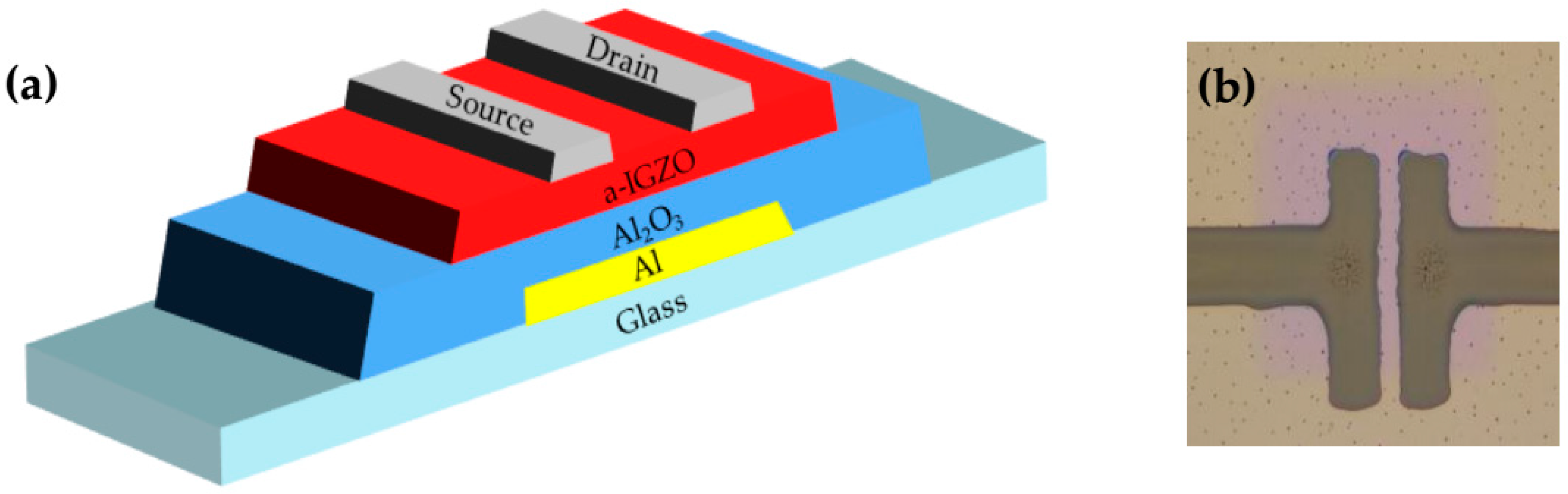
The cross-sectional of a-IGZO TFT with inkjet-printed silver S/D electrodes is illustrated in
Figure 1a. The fabrication processes are given as follows: firstly, a 300-nm-thick Al gate was deposited on cleaned glass by DC sputtering and patterned by wet etching. Subsequently, the film was anodized in the electrolyte consisting of an ammonium tartrate solution and ethylene glycol. As a result, a 200-nm-thick Al
2O
3 insulator gate was formed in an electrolyte consisting of a 3.68 wt % ammonium tartrate solution and ethylene glycol on the Al gate. After that, a 25-nm-thick a-IGZO film patterned via shadow mask was deposited on the insulating layer by RF magnetron sputtering, and the obtained device was annealed at 400 °C for 1 h under atmospheric conditions. At last, a printing process was employed to form the silver source and drain electrodes, which is shown in
Figure 1b.
The silver ink (30%–35% in volume) for the electrodes consists of silver nanoparticles (30–50 nm) and alcohol-based solvent (DGP 40TE-20C, Advanced Nano Products, Bugang-myeon, Sejong-si, Korea). The silver S/D electrode was printed onto the a-IGZO layers through an inkjet printer with a 10 pL print head driven by piezoelectricity (Fujifilm Dimatix, DMP2800, Santa Clara, CA, USA). Ag ink was printed using an optimized wave form and cartridge temperature of 30 °C. The droplets were deposited with a dot spacing of 35 μm and resulted in a smaller channel width/length of 551.29 µm/31.09 µm. After printing, UV curing equipment was used to dry the Ag ink with the condition of 100% intensity for 180 s in air.
The dimensions of the printed electrodes were measured by a Nikon Eclipse E600 POL with a DXM1200F digital camera (Nikon, DeWitt, IA, USA). TFT properties were studied using a semiconductor parameter analyzer (Agilent 4155C, Santa Clara, CA, USA) under ambient condition. TEM with an energy dispersive X-ray spectrometer (EDS, Bruker, Adlershof, Berlin, Germany) was used to analyze the distribution of elements, and carbon was detected by EELS (Electron Energy Loss Spectroscopy, Gatan Enfinium ER Model 977, Pleasanton, CA, USA).
3. Results and Discussion
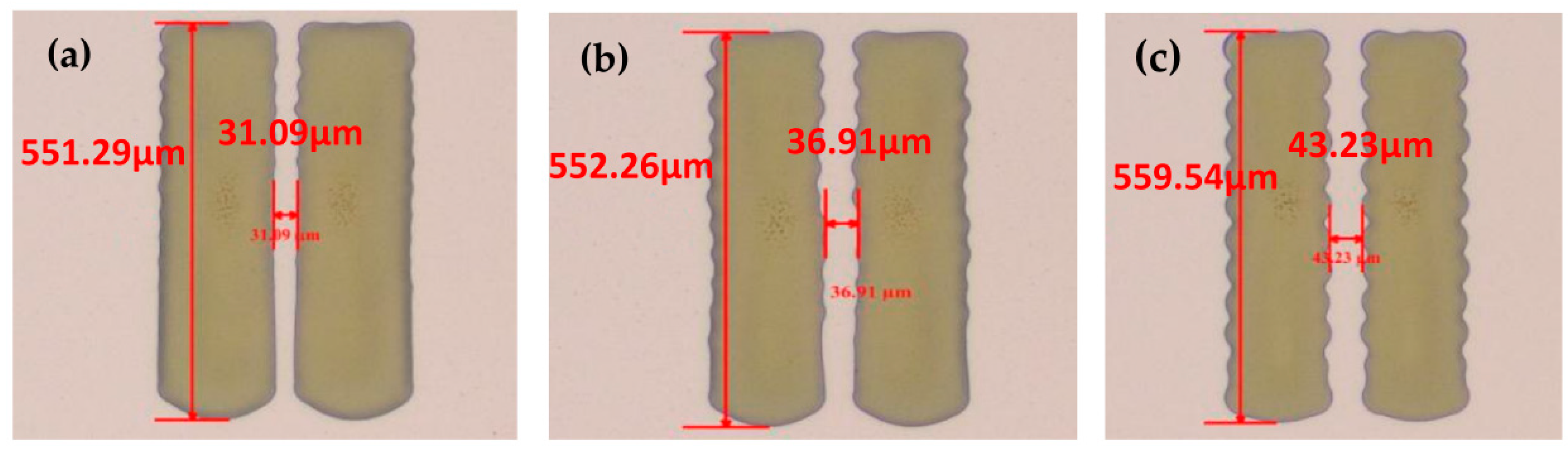
The silver S/D electrodes with different dot spacing were inkjet-printed on the a-IGZO layer by controlling the droplet spacing. As we can see from
Figure 2, the length of the channel increased with the increase in dot spacing. The wavy edge became distinct as the drop space increased. In order to avoid the influence of the edges and obtain a smaller channel length, 35 µm dot spacing was set.
At first, a-IGZO TFTs with printed S/D electrodes were manufactured at room temperature.
Figure 3a,b show output characteristic curves (I
DS–V
DS) and transfer characteristic curves (I
DS–V
GS), respectively. In our work, the gate voltage (V
GS) was changed from 0 to 20 V in steps of 5 V. The transfer curves were tested with a V
DS of 10.1 V and a V
GS from 20 to −20 V. A low source/drain current was indicated in the I
DS–V
DS and I
DS–V
GS curves. We suggested the existence of poor interfacial contact and/or serious diffusion between the active layer and the silver electrodes because of the organic solvent. It is quite important to reduce the carbon concentration in the solvent, as reported in [
24]. Therefore, we decided to increase the printing substrate temperature. With the increase in substrate temperature up to 50 °C, no obvious improvement on the TFT properties was observed (see in
Figure S1), but the TFT exhibits excellent output characteristics in the linear regime from
Figure 3a at an equipment limited substrate temperature of 60 °C, and shows better transfer characteristics than the TFTs printed at lower temperature. It enables a mobility of 0.29 cm
2·V
−1·s
−1 and an on/off current ratio over 10
5, which is a major improvement for a-IGZO TFTs with printed silver electrodes that was reported so far (see
Figures S2 and S3). This result clearly indicates good contact between the IGZO and the Ag.
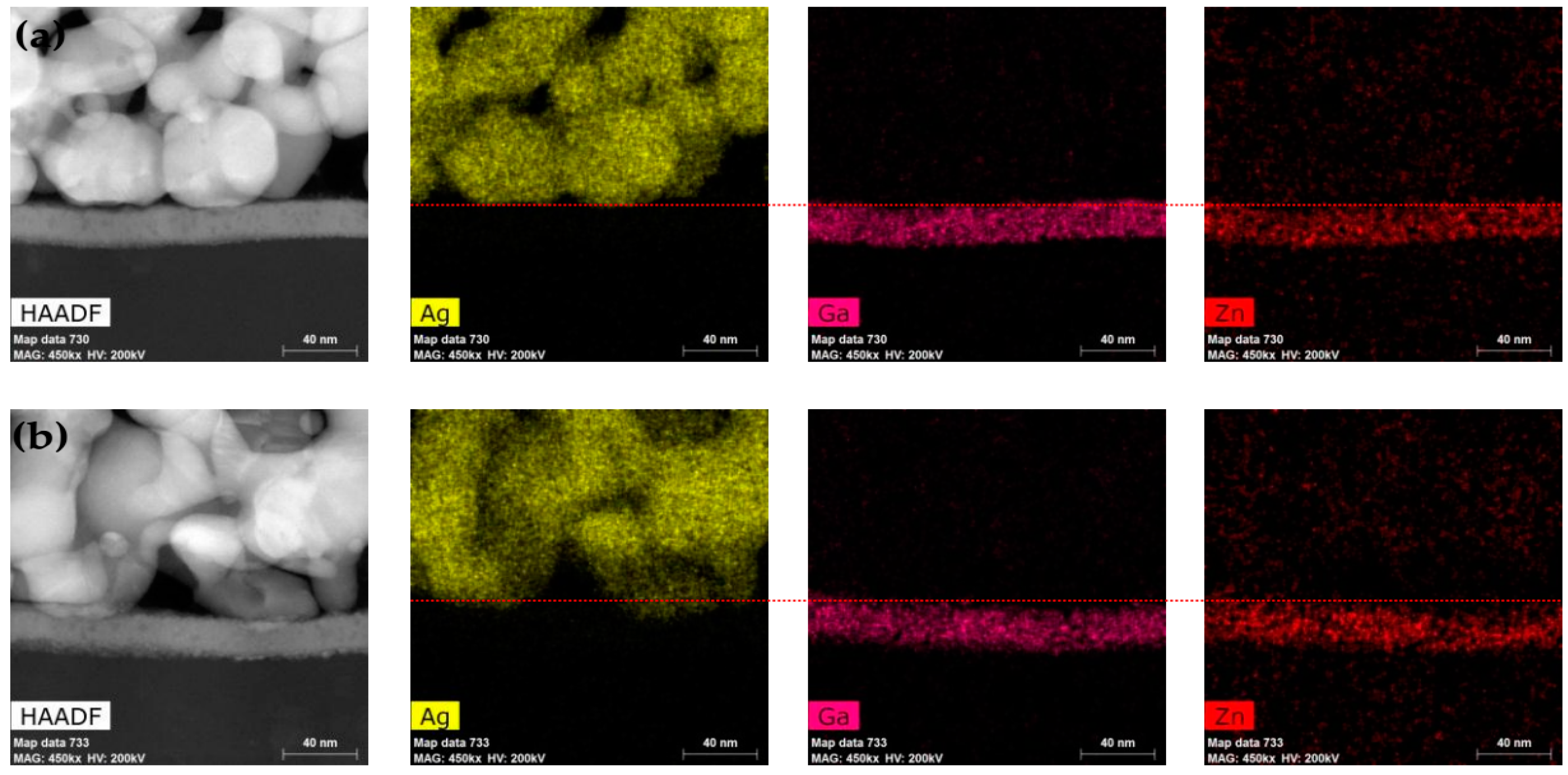
To figure out the mechanism that leads to different TFT characteristics, TEM (transmission electron microscope) with an energy dispersive X-ray spectrometer (EDS) was used to observe the interface and detect the distribution of elements after the sample was prepared by a FIB (focused ion beam, FEI Helios 450S dual beam FIB, Milpitas, CA, USA). A clear morphology of Ag particles when printing at room temperature can be observed in
Figure 4a. Nanoparticles start melting at a low temperature due to its high surface energy and nanoscale [
25]. Therefore, the cross-sectional images in
Figure 4 demonstrate the Ag particles merged together at a substrate temperature of 60 °C. As we know, Ag nanoparticles are dispersed by a dispersant, which means the particles are surrounded with organics [
26,
27]. From
Figure 4b, we can see clearly that Ag particles diffused into a-IGZO layers, which contributes to a good contact that finally results in better TFT characteristics.
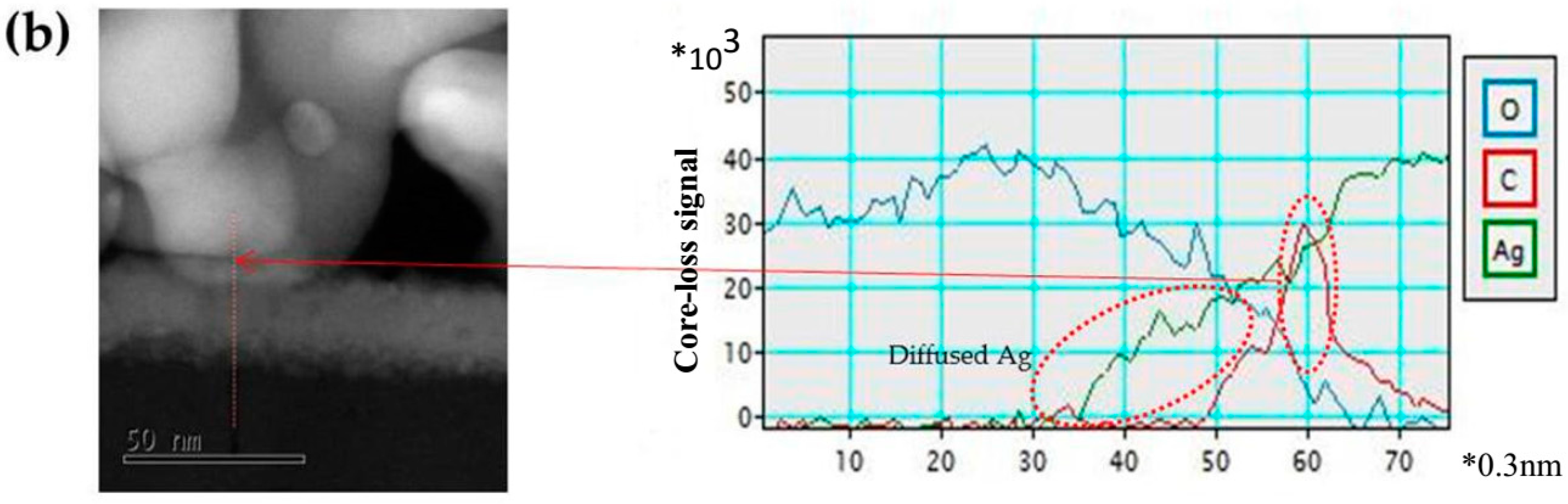
As shown in
Figure 5a, a considerable amount of carbon was detected at the interface between Ag and a-IGZO, which reveals the existence of an organic layer that blocks the transportation of electrons. However, for the Ag electrodes printed on a-IGZO with a temperature of 60 °C, no carbon was observed at the interface (
Figure 5b)—carbon was only detected on the surface of the Ag particles. Therefore, we can safely conclude that a thin organic layer at the interface isolates the Ag electrodes from a-IGZO, which leads to poor TFT characteristics when printing at lower temperatures. With the increase of the substrate temperature up to 60 °C, Ag nanoparticles melt, and it is beneficial for Ag to diffuse into a-IGZO. Although a few Ag nanoparticles could diffuse into a-IGZO, desirable TFT characteristics were achieved.
4. Conclusions
In summary, we achieved desirable TFT characteristics with inkjet-printed Ag S/D electrodes on an a-IGZO layer by increasing the substrate temperature. According to the FIB-TEM results, carbon was detected at the interface between Ag and the a-IGZO, and there was poor contact when the Ag electrodes were printed on the a-IGZO layer at room temperature. As the substrate temperature increased, however, Ag nanoparticles adjacent to the interface merged together and diffused into a-IGZO, resulting in a better contact at the interface. As a result, the device exhibits a mobility of 0.29 cm2·V−1·s−1 and an on/off current ratio of over 105. This study proves the possibility of directly inkjet printing silver electrodes on a-IGZO layer to fabricate TFTs with desirable device performance.
Supplementary Materials
The following are available online at
www.mdpi.com/1996-1944/10/1/51/s1. Figure S1: Output characteristic curves (I
DS–V
DS) and transfer characteristic curve (I
DS–V
GS) of manufactured a-IGZO TFTs at different printing substrate temperatures. (a) 40 °C; (b) 50 °C; (c) 40 °C; (d) 50 °C. VGS is varied from 20 to −20 V with VDS = 10.1 V, Figure S2: Transfer characteristic curve (I
DS–V
GS) of devices Yoshihiro et al. had reported, Figure S3: Transfer characteristic curve (I
DS–V
GS) of devices Ethan et al. had reported.
Acknowledgments
This work was supported by the National Key Research and Development Program of China (No. 2016YFB0401504 and 2016YFF0203603), the National Key Basic Research and Development Program of China (973 program, Grant No. 2015CB655004) founded by MOST, the Guangdong Natural Science Foundation (No. 2016A030313459), the Science and Technology Project of Guangdong Province (No. 2014B090915004, 2014A040401014, 2016A040403037, 2016B090907001, and 2016B090906002), the Fundamental Research Funds for the Central Universities (No. 2015ZP024 and 2015ZZ063), the State Key Laboratory of Luminescence and Applications (SKLA-2016-11), and the Open Funds of Key Laboratory of Advanced Display and System Applications, Shanghai University, China (P201605).
Author Contributions
Honglong Ning, Rihui Yao, Ruiqiang Tao and Jianqiu Chen conceived and designed the experiments; Jianqiu Chen, Wei Cai and Shiben Hu performed the experiments; Zhennan Zhu, Yicong Zhou, Caigui Yang, analyzed the data; Junbiao Peng, Honglong Ning, and Rihui Yao provided valuable discussions and suggestions; Honglong Ning, Jianqiu Chen and Zhiqiang Fang wrote the paper.
Conflicts of Interest
The authors declare no conflict of interest.
References
- Park, J.S.; Maeng, W.; Kim, H.; Park, J. Review of recent developments in amorphous oxide semiconductor thin-film transistor devices. Thin Solid Films 2012, 520, 1679–1693. [Google Scholar] [CrossRef]
- Choi, C.H.; Lin, L.Y.; Cheng, C.C.; Chang, C.H. Printed Oxide Thin Film Transistors: A Mini Review. ECS J. Solid State Sci. Technol. 2015, 4, P3044–P3051. [Google Scholar]
- Franklin, A.D. DEVICE TECHNOLOGY. Nanomaterials in transistors: From high-performance to thin-film applications. Science 2015, 349, aab2750. [Google Scholar] [CrossRef] [PubMed]
- Wu, Y.; Li, Y.; Ong, B.S. A Simple and Efficient Approach to a Printable Silver Conductor for Printed Electronics. J. Am. Chem. Soc. 2007, 129, 1862–1863. [Google Scholar] [CrossRef] [PubMed]
- Ning, H.; Tao, R.; Fang, Z.; Cai, W.; Chen, J.; Zhou, Y.; Zhu, Z.; Zheng, Z.; Yao, R.; Xu, M.; et al. Direct patterning of silver electrodes with 2.4 μm channel length by piezoelectric inkjet printing. J. Colloid Interface Sci. 2017, 487, 68–72. [Google Scholar] [CrossRef] [PubMed]
- Zhang, Z.; Zhang, X.; Xin, Z.; Deng, M.; Wen, Y.; Song, Y. Controlled Inkjetting of a Conductive Pattern of Silver Nanoparticles Based on the Coffee-Ring Effect. Adv. Mater. 2013, 25, 6714–6718. [Google Scholar] [CrossRef] [PubMed]
- Gelinck, G.H.; Geuns, T.C.T.; De Leeuw, D.M. High-performance all-polymer integrated circuits. Appl. Phys. Lett. 2000, 77, 1487–1489. [Google Scholar] [CrossRef]
- Lu, G.; Usta, H.; Risko, C.; Wang, L.; Facchetti, A.; Ratner, M.A.; Marks, T.J. Synthesis, characterization, and transistor response of semiconducting silole polymers with substantial hole mobility and air stability. Experiment and theory. J. Am. Chem. Soc. 2008, 130, 7670–7685. [Google Scholar] [CrossRef] [PubMed]
- Castro, H.F.; Sowade, E.; Rocha, J.G.; Alpuim, P.; Lanceros-Méndez, S.; Baumann, R.R. All-Inkjet-Printed Bottom-Gate Thin-Film Transistors Using UV Curable Dielectric for Well-Defined Source-Drain Electrodes. J. Electron. Mater. 2014, 43, 2631–2636. [Google Scholar] [CrossRef]
- Kim, D.; Jeong, S.; Lee, S.; Park, B.K.; Moon, J. Organic thin film transistor using silver electrodes by the ink-jet printing technology. Thin Solid Films 2007, 515, 7692–7696. [Google Scholar] [CrossRef]
- Fukuda, K.; Sekine, T.; Kumaki, D.; Tokito, S. Profile Control of Inkjet Printed Silver Electrodes and Their Application to Organic Transistors. ACS Appl. Mater. Interfaces 2013, 5, 3916–3920. [Google Scholar] [CrossRef] [PubMed]
- Kawase, T.; Shimoda, T.; Newsome, C.; Sirringhaus, H.; Friend, R.H. Inkjet printing of polymer thin film transistors. Thin Solid Films 2003, 438–439, 279–287. [Google Scholar] [CrossRef]
- Noguchi, Y.; Sekitani, T.; Yokota, T.; Someya, T. Direct inkjet printing of silver electrodes on organic semiconductors for thin-film transistors with top contact geometry. Appl. Phys. Lett. 2008, 93, 43303. [Google Scholar] [CrossRef]
- Kim, D.; Jeong, S.; Moon, J.; Han, S.; Chung, J. Organic thin film transistors with ink-jet printed metal nanoparticle electrodes of a reduced channel length by laser ablation. Appl. Phys. Lett. 2007, 91, 71114. [Google Scholar] [CrossRef]
- Zhou, L.; Han, S.T.; Zhuang, J.; Yan, Y.; Zhou, Y.; Sun, Q.J.; Xu, Z.X.; Roy, V.A.L. Mobility Enhancement of P3HT-Based OTFTs upon Blending with Au Nanorods. Part. Part. Syst. Charact. 2015, 32, 1051–1057. [Google Scholar] [CrossRef]
- Sun, B.; Hong, W.; Aziz, H.; Li, Y.; Hong, W. A pyridine-flanked diketopyrrolopyrrole (DPP)-based donor-acceptor polymer showing high mobility in ambipolar and n-channel organic thin film transistors. Polym. Chem. UK 2014, 6, 938–945. [Google Scholar] [CrossRef]
- Hu, S.; Fang, Z.; Ning, H.; Tao, R.; Liu, X.; Zeng, Y.; Yao, R.; Huang, F.; Li, Z.; Xu, M.; et al. Effect of Post Treatment For Cu-Cr Source/Drain Electrodes on a-IGZO TFTs. Materials 2016, 9, 623. [Google Scholar] [CrossRef]
- Choi, K.; Kim, H. Correlation between Ti source/drain contact and performance of InGaZnO-based thin film transistors. Appl. Phys. Lett. 2013, 102, 52103. [Google Scholar] [CrossRef]
- Ueoka, Y.; Ishikawa, Y.; Bermundo, J.P.; Yamazaki, H.; Urakawa, S.; Osada, Y.; Horita, M.; Uraoka, Y. Effect of contact material on amorphous InGaZnO thin-film transistor characteristics. Jpn. J. Appl. Phys. 2014, 53, 3C–4C. [Google Scholar] [CrossRef]
- Wu, Q.; Xu, L.; Xu, J.; Xie, H.; Dong, C. Amorphous InGaZnO thin film transistors with sputtered silver source/drain and gate electrodes. Mater. Sci. Semicond. Process. 2016, 48, 23–26. [Google Scholar] [CrossRef]
- Pudasaini, P.R.; Noh, J.H.; Wong, A.T.; Ovchinnikova, O.S.; Haglund, A.V.; Dai, S.; Ward, T.Z.; Mandrus, D.; Rack, P.D. Ionic Liquid Activation of Amorphous Metal-Oxide Semiconductors for Flexible Transparent Electronic Devices. Adv. Funct. Mater. 2016, 26, 2820–2825. [Google Scholar] [CrossRef]
- Pudasaini, P.R.; Noh, J.H.; Wong, A.; Haglund, A.V.; Dai, S.; Ward, T.Z.; Mandrus, D.; Rack, P.D. Ionic Liquid versus SiO2 Gated a-IGZO Thin Film Transistors: A Direct Comparison. J. Solid State Sci. Technol. 2015, 4, Q105–Q109. [Google Scholar] [CrossRef]
- Secor, E.B.; Smith, J.; Marks, T.J.; Hersam, M.C. High-Performance Inkjet-Printed Indium-Gallium-Zinc-Oxide Transistors Enabled by Embedded, Chemically Stable Graphene Electrodes. ACS Appl. Mater. Interfaces 2016, 8, 17428–17434. [Google Scholar] [CrossRef] [PubMed]
- Ueoka, Y.; Nishibayashi, T.; Ishikawa, Y.; Yamazaki, H.; Osada, Y. Analysis of printed silver electrode on amorphous indium gallium zinc oxide. Jpn. J. Appl. Phys. 2014, 53, 04EB03. [Google Scholar] [CrossRef]
- Moon, K.; Dong, H.; Maric, R.; Pothukuchi, S.; Hunt, A.; Li, Y.; Wong, C.P. Thermal behavior of silver nanoparticles for low-temperature interconnect applications. J. Electron. Mater. 2005, 34, 168–175. [Google Scholar] [CrossRef]
- Sondi, I.; Goia, D.V.; Matijević, E. Preparation of highly concentrated stable dispersions of uniform silver nanoparticles. J. Colloid Interface Sci. 2003, 260, 75–81. [Google Scholar] [CrossRef]
- Wang, H.; Qiao, X.; Chen, J.; Wang, X.; Ding, S. Mechanisms of PVP in the preparation of silver nanoparticles. Mater. Chem. Phys. 2005, 94, 449–453. [Google Scholar] [CrossRef]
© 2017 by the authors. Licensee MDPI, Basel, Switzerland. This article is an open access article distributed under the terms and conditions of the Creative Commons Attribution (CC-BY) license ( http://creativecommons.org/licenses/by/4.0/).


 ,
, 

