Article

A New Switching Impulse Generator Based on Transformer Boosting and Insulated Gate Bipolar Transistor Trigger Control

1
State Key Laboratory of Electrical Insulation and Power Equipment, Xi’an Jiaotong University, Xi’an 710049, China
2
Department of Electrical, Electronics and Automation Engineering and Applied Physics, Polytechnic University of Madrid, Ronda de Valencia 3, Madrid 28012, Spain
*
Author to whom correspondence should be addressed.
Energies 2016, 9(8), 644; https://doi.org/10.3390/en9080644
Submission received: 2 June 2016 / Revised: 5 August 2016 / Accepted: 8 August 2016 / Published: 16 August 2016

Abstract

:
To make the switching impulse (SI) generator more compact, portable and feasible in field tests, a new approach based on transformer boosting was developed. To address problems such as triggering synchronization and electromagnetic interference involved with the traditional spark gap, an insulated gate bipolar transistor (IGBT) module with drive circuit was employed as the impulse trigger. An optimization design for the component parameters of the primary winding side of the transformer was realized by numerical calculation and error correction. Experiment showed that the waveform parameters of SI and oscillating switching impulse (OSI) voltages generated by the new generator were consistent with the numerical calculation and the error correction. The generator was finally built on a removable high voltage transformer with small size. Thus the volume of the generator is significantly reduced. Experiments showed that the waveform parameters of SI and OSI voltages generated by the new generator were basically consistent with the numerical calculation and the error correction.

Graphical Abstract

1. Introduction

On account of the frequent failures of high voltage power equipment [1,2,3], more attention has been increasingly focused on the impulse withstand voltage test in the field [4], which has become a more stringent and effective method of evaluating the insulation status of power equipment [5,6,7,8]. The traditional impulse generator is built on a Marx circuit, which has been widely applied in high voltage testing and insulation assess for many years. However, the Marx generator is labor intensive and time consuming in replacing the output waveform, and its multiple spark airgap switches are sometimes triggered out of synchrony, especially when the preset voltage is not very high. In addition, electromagnetic interference [9] that arises from the spark discharge makes partial discharge detection difficult. In this study, we tried to use an impulse transformer to magnify the input impulse voltage. The entire equivalent circuit model was analytically analyzed to accurately control the generator output by adjusting only the circuit connected to the primary winding side, and on this basis, a parameter optimization method was proposed.
In addition, instead of the spark gap of the Marx generator, an insulated gate bipolar transistor (IGBT) was used as a trigger switch owing to its good performance in turning on and cutting off the current with a rapid response time and low noise at the instant of triggering. In this study, the generating circuit of the switching impulse (SI) voltage was initially designed, and its circuit parameters were solved by analytical calculation. Subsequently, the influence of the circuit component parameters on the waveform parameters was analyzed, and an optimized method to select the component parameters was proposed. Finally, aperiodic SI voltage and oscillating switching impulse (OSI) voltage were successfully generated by a 50 kV transformer. Moreover, some technical considerations were discussed for improving the output voltage, increasing output power capacity, as well as generating lightning impulse voltage.

2. Principle of Transformer Boosting-Based Impulse Generation

To establish a guide for designing the primary winding side circuit and determining the circuit parameters based on transformer induction, this section first proposed a fourth-order equivalent circuit to generate a SI According to the solution, waveform parameters in pace with variations of the circuit parameters were obtained by calculation. Subsequently, an optimization method was proposed to select the circuit parameters by considering the waveform error (S) and impulse magnification ratio (IMR).

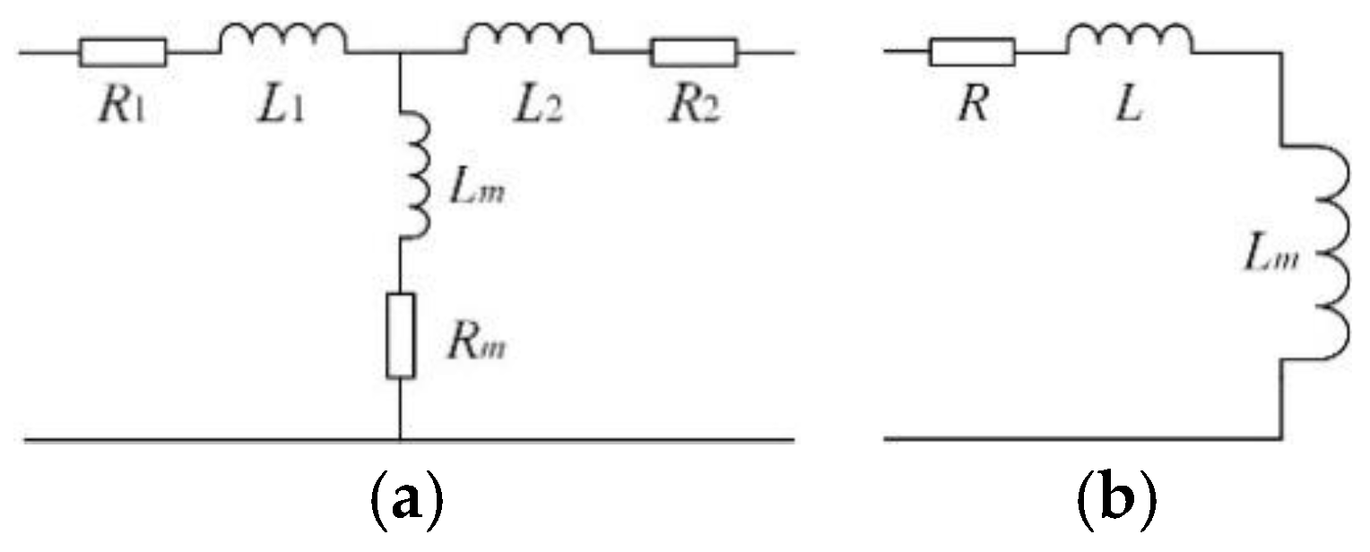
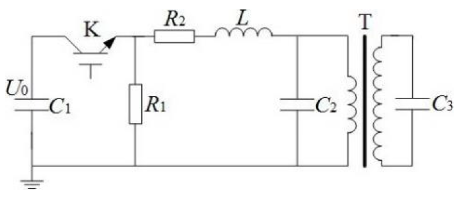
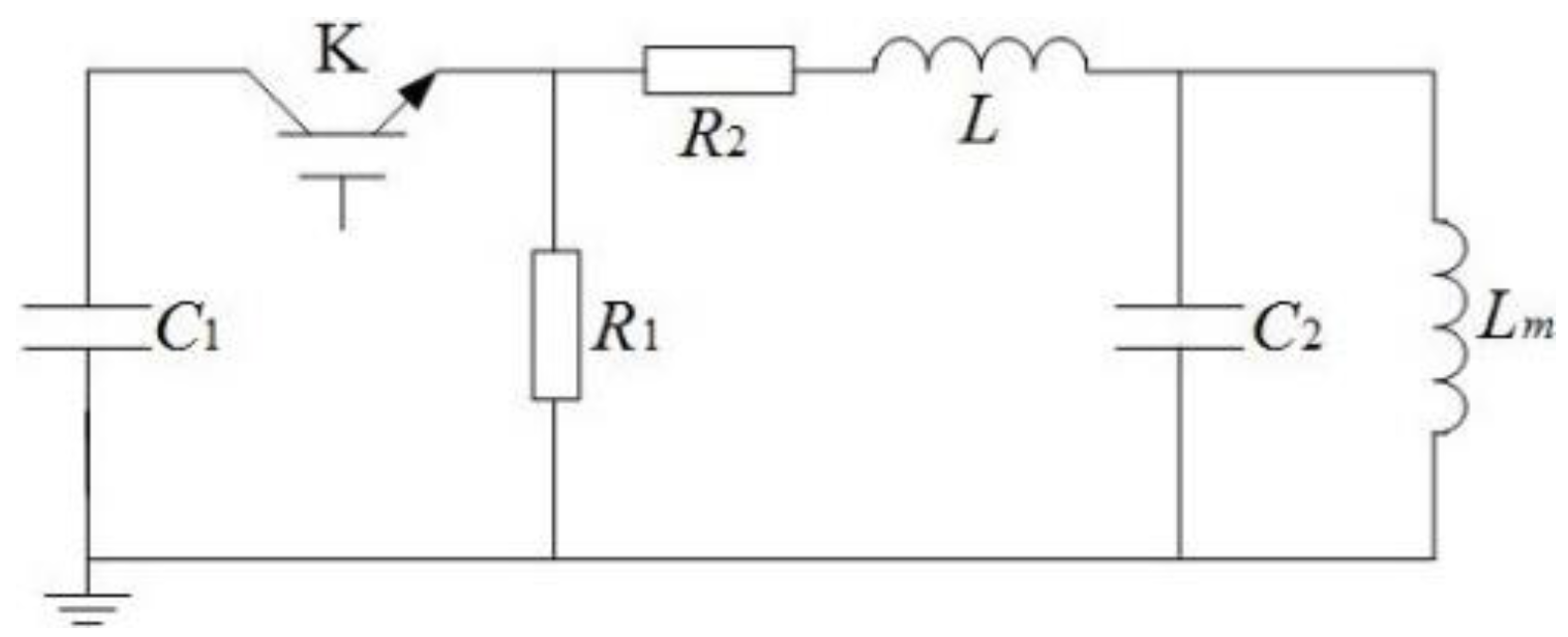
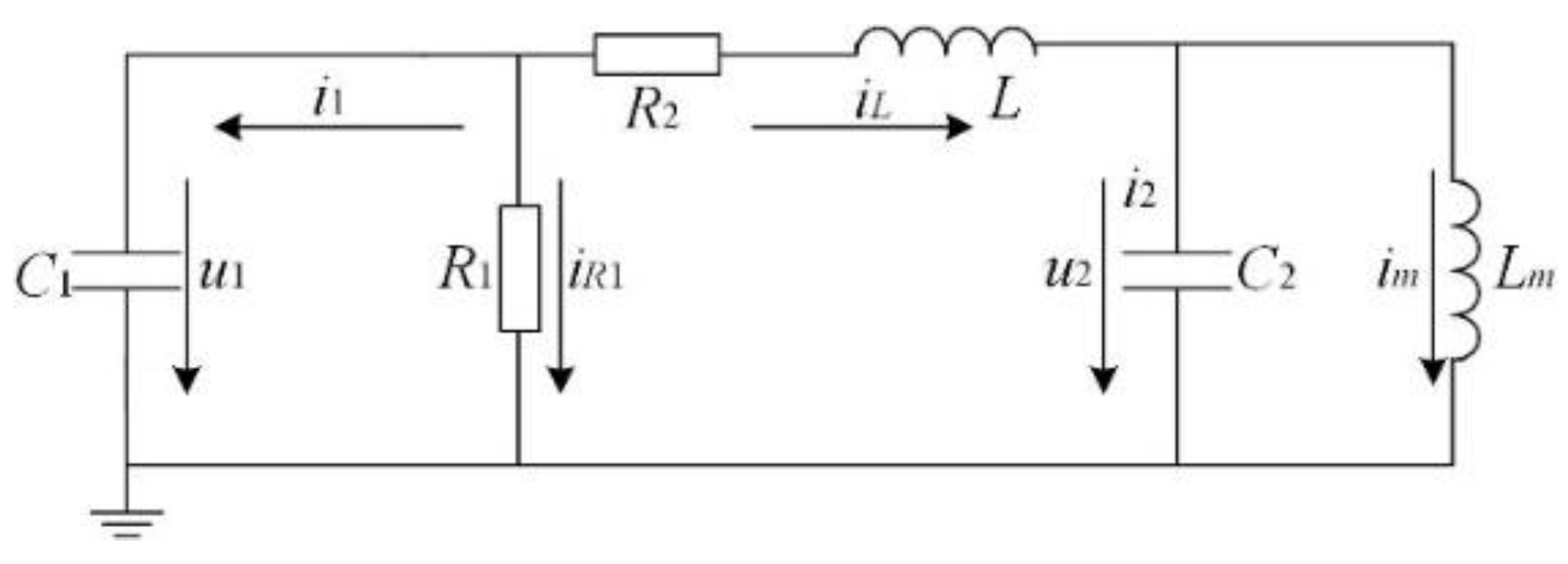
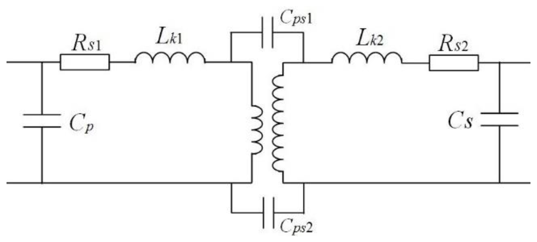
2.1. Equivalent Circuit Analysis

The basic idea for generating an impulse is to input a small impulse into the primary side of a transformer and thus to obtain an amplified impulse at the secondary (high-voltage) side. To achieve a more effective on-off trigger control, the traditional spark gap is replaced with an IGBT module.
The circuit diagram of the principle for generating SI is sketched as shown in Figure 1. Here, power electronic switch K initially stays in the off state as a trigger switch, U0 is the voltage on C1 after charging, and L is the wave-modulating inductor for generating an OSI voltage (it is not adopted to generate SI). As the trigger switch is turned on, main capacitor C1 discharges to wave-modulating capacitor C2, which is connected in parallel with the primary side of the transformer, and a high-amplitude SI voltage is induced at the secondary side.
The single-phase transformer shown in Figure 1 can be represented by an equivalent T-type circuit, as shown in Figure 2a. Considering that the winding resistance of the test transformer is relatively smaller than the reactance and that the leakage resistance is much smaller than the excitation reactance, the transformer can be represented by an equivalent Γ-type circuit (Figure 2b) [10].
The entire equivalent discharge circuit of the SI voltage is shown in Figure 3. Here, L is the total equivalent inductance of the wave-modulating and the leakage inductance, and C2 is the total equivalent capacitance of the load and the wave-modulating capacitance.

2.2. Numerical Calculation

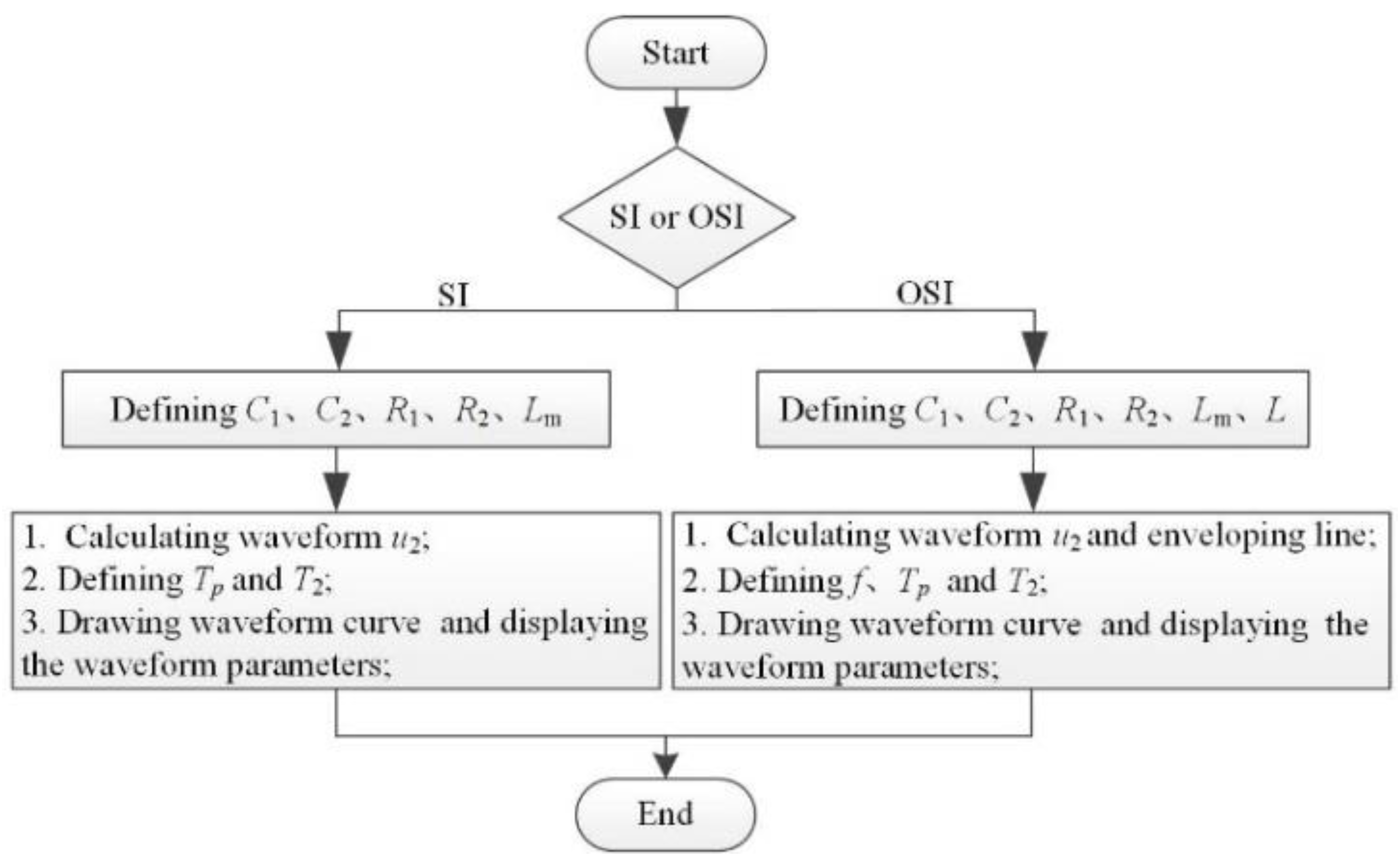
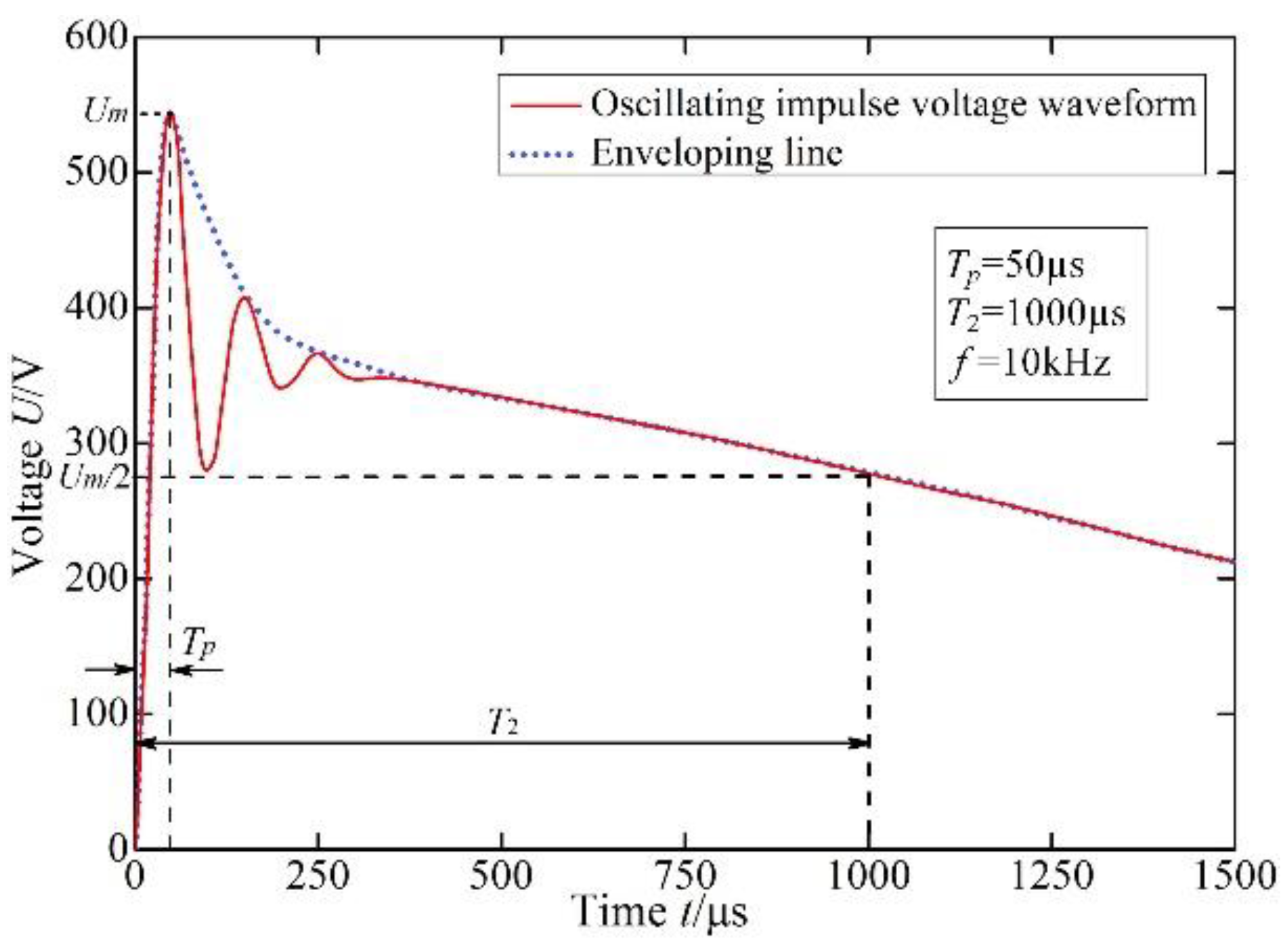
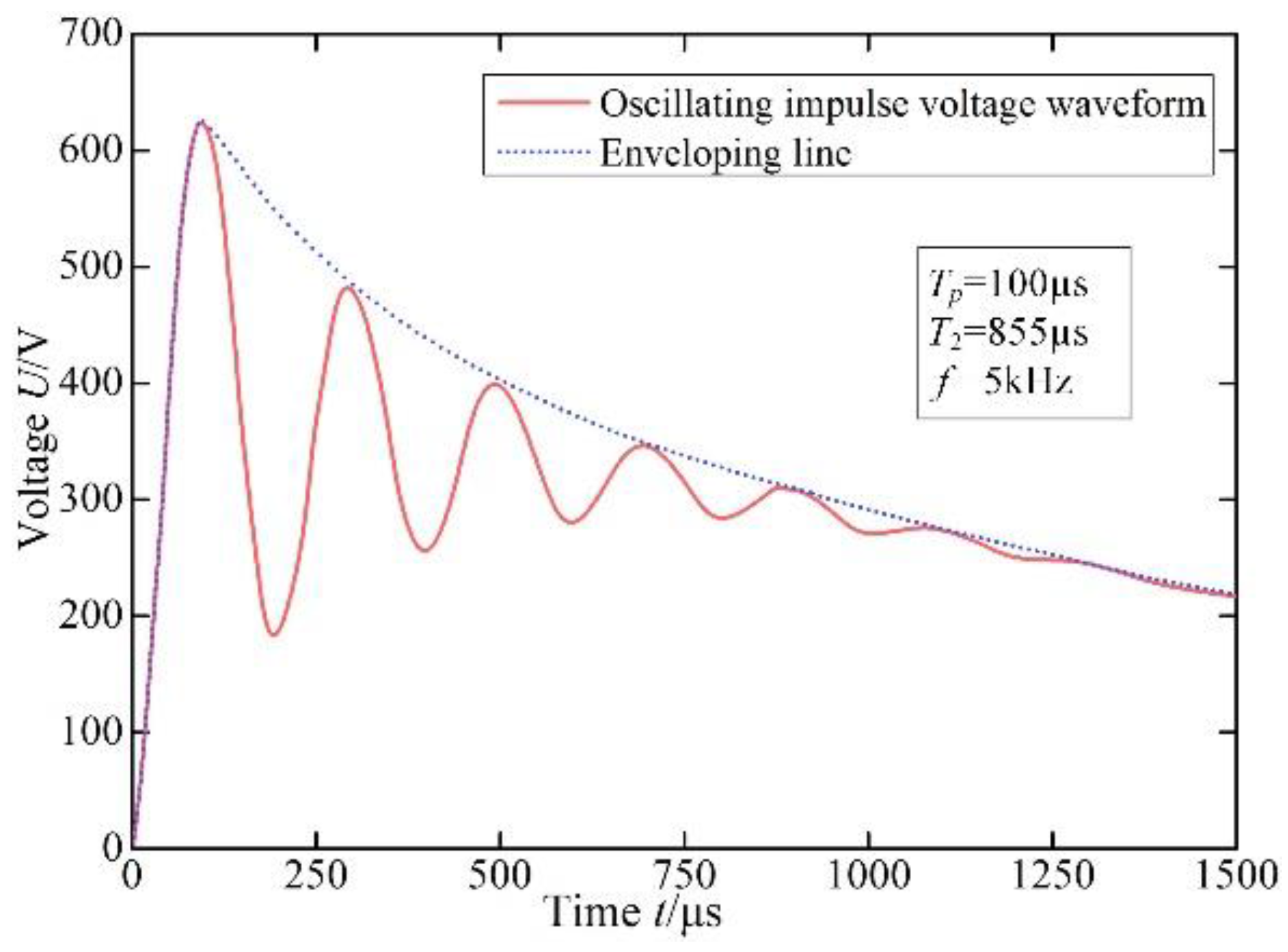
2.2.1. Oscillating Switching Impulse Voltage

According to the equivalent circuit previously mentioned, the equivalent circuit of the entire system configuration during discharge can be drawn as shown in Figure 4.
The loop equation of the equivalent circuit can be expressed by Equation (1) in a fourth-order form:
L L m C 1 C 2 d 4 i m d t 4 + ( C 1 C 2 R 2 L m + L C 2 L m R 1 ) d 3 i m d t 3 + ( L C 1 + L m C 1 + L m C 2 R 2 R 1 + L m C 2 ) d 2 i m d t 2 + ( C 1 R 2 + L R 1 + L m R 1 ) d i m d t + R 2 + R 1 R 1 i m = 0
The initial conditions for Equation (1) are described in Equation (2):
{ i m | t = 0 = 0 d i m d t | t = 0 = 0 d 2 i m d t 2 | t = 0 = 0 d 3 i m d t 3 | t = 0 = U 0 L L m C 2
Indeed, it is very difficult to obtain the explicit analytical expression for a fourth-order equation [11]. To accurately analyze the relationships between the circuit parameters and waveform parameters, the fourth-order Runge-Kutta method was applied to solve these ordinary differential equations [12,13,14]. For Equation (1), the ordinary differential equations can be solved by introducing an intermediate variable, as expressed in Equation (3):
y = F y
here:
y = ( y 1 , y 2 , y 3 , y 4 ) T , y = ( y 1 , y 2 , y 3 , y 4 ) T
and the coefficient matrix is expressed in Equations (5) and (6):
F = [ 0 1 0 0 0 0 1 0 0 0 0 1 e a d a c a b a ] ,   y 0 = ( 0 , 0 , 0 , U 0 L L m C 2 ) T
{ a = L L m C 1 C 2 b = C 1 C 2 R 2 L m + L C 2 L m R 1 c = L C 1 + L m C 1 + L m R 1 R 2 R 1 + L m C 2 d = C 1 R 2 + L R 1 + L m R 1 e = R 2 + R 1 R 1   { y 1 = i m y 1 = d i m d t = y 2 y 2 = d 2 i m d t 2 = y 3 y 3 = d 3 i m d t 3 = y 4 y 4 = b a y 4 c a y 3 d a y 2 e a y 1
The solution vector y in Equation (3) can be solved by the fourth-order Runge–Kutta equation, and curve u2 of the OSI waveform can be obtained by Equation (7):
u 2 = L m d i m d t = L m y 2

2.2.2. Switching Impulse Voltage

The analysis method for SI is similar to that for the OSI, and the only difference from the consideration of the OSI is that the wave-modulating inductance in the primary side is not needed, i.e., L = 0; hence, the circuit can be described by a group of third-order differential equations.

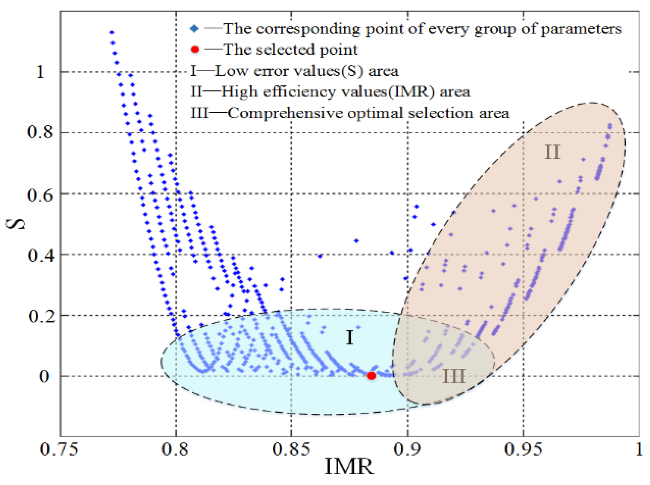
2.3. Selection and Optimization of the Circuit Parameters

Based on the analytical solution of the circuit parameters, the key parameters of the waveform can be determined with numerical computing, such as peak time Tp, half-peak time T2, enveloping line, and oscillation frequency f. Assuming that Tp and T2 of the target impulse voltage are Tp’ and T2’, respectively, the waveform error S can be calculated by Equation (8):
S = ( T p T p ) 2 T p 2 + ( T 2 T 2 ) 2 T 2 2
Apparently, the smaller S is, the closer is the calculated waveform to the target waveform. Consequently, optimal parameters of the component and their combination within a certain range and a minimum S are expected. In addition, the output efficiency of the generator should be taken into consideration. IMR is thus introduced to generally evaluate the output efficiency of this SI voltage generator, as expressed by Equation (9):
I M R = U m U 1
Here, Um is the amplitude of the output voltage, and U1 is the charging voltage on C1. In fact, the circuit parameters can hardly meet both the requirements for minimum S and maximum IMR simultaneously. Therefore, the selection of the final circuit parameters is a result of a tradeoff between the two key parameters.

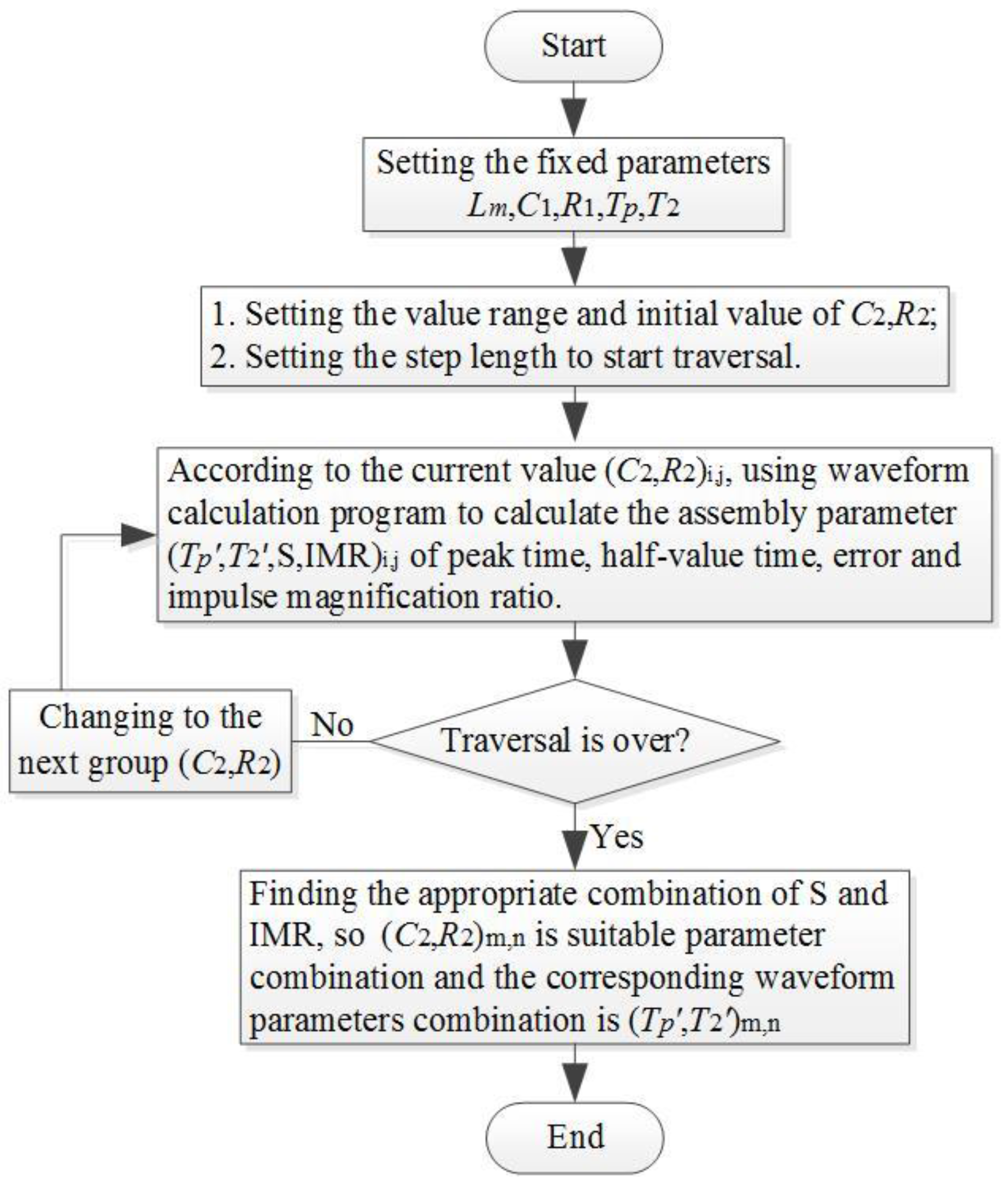
2.3.1. Solving the Circuit Parameters for the Given Target Waveform Parameters

The main program and subprogram flowcharts to calculate the circuit parameters are shown in Figure 5 and Figure 6, respectively. Here, the subprogram is used to calculate the waveform curves and parameters using the given circuit component parameters. Initially, parameters C1, Lm and R1 are set to fixed values that can hardly be adjusted in practice, and the specific parameters of the target waveform, such as Tp and T2, are provided. Then, the expected value ranges for C2, L and R2 within a group of parameters such as Tp, T2, S and IMR can be estimated several times by circular computation using the initial value and step length.
Figure 7 shows an example of the S-IMR distribution which can be used for the parameter optimization. Area I in Figure 7 is composed of parameter combinations with small errors. Area II of the parameter combinations with large IMRs and Area III of the intersection of Areas I and II provides the comprehensive optimal selection area in this distribution. In this area, the circuit parameters are given priority with an optimized combination of larger IMR and small error.

2.3.2. Impulse Waveforms Solution Using the Given Circuit Parameters

To more intuitively describe the influence of the circuit parameters on the impulse waveform, the calculation results are illustrated by discussing the SI and OSI voltages.
  • Switching impulse voltage
If the circuit parameters are given as L = 0, C1 = 10 µF, C2 = 1 µF, Lm = 0.9 H, R1 = 1155 Ω, R2 = 56 Ω and Uc1 = 400 V, the corresponding SI could satisfy the waveform parameters recommended by the IEC 60060-3 standard [4] (i.e., Tp = 250 μs and T2 = 2500 μs), as shown in Figure 6. By changing a single variable, we can observe the variations in Tp, T2 and Um with decreasing Lm and increasing C1, C2, R1 and R2, as shown in Figure 8. The corresponding parameters are listed in Table 1.
Figure 8 and Table 1 show that both Tp and T2 decrease with the decrease in Lm. Meanwhile, Tp, T2, and IMR increase with the increase in C1. The increases in Tp, T2, and IMR are not sensitive to the increase in R1. Tp and T2 obviously change along with the changes in R2 and C2. Further, a positive correlation exists between Tp and R2, C2, whereas T2 shows a positive correlation with C2 and a negative correlation with R2. Therefore, adjusting the element parameters of C2 and R2 is preferable in practice. Because Lm is an inherent parameter of the transformer and has a nonlinear characteristic with the magnetizing current, the nonlinear curve of Lm should be introduced in every step of the calculation to obtain a simulation result closer to the real output.
  • Oscillating switching impulse voltage
An OSI waveform is generated when the circuit is underdamped (i.e., R 2 < 2 [ L ( C 1 + C 2 ) / C 1 C 2 ] 1 ). If the circuit parameters are given as the combination of C1 = 3 μF, C2 = 0.22 μF, Lm = 1.3 H, R1 = 2230 Ω, R2 = 33 Ω and L = 1.2 mH, the OSI waveform has Tp of 50 μs, T2 of 1000 μs, Um of 556.0 V and f of 10 kHz, as shown in Figure 9. As L increases, the waveform oscillation becomes more serious, as shown in Figure 10. Some simulations performed by changing circuit parameters C1, C2, R1 and R2 are listed in Table 2.
The oscillation frequency of OSI is related to both parameters L, C1, C2 and R2. When R2 is very small, f is determined by the combination of L, C1 and C2, as expressed in Equation (10). Tp is actually half of the oscillation period.
f = 1 2 T p = 1 2 π C 1 + C 2 L C 1 C 2
When R2 increases to a critical damping condition (even to an overdamped condition), the waveform stops oscillating. Therefore, the OSI waveform can be converted to an SI waveform by reducing L or improving R2. In addition, T2 increases with the increase in C1, C2, R1 and R2, and slightly decreases with the increase in L.
Similar to SI, IMR can be improved by increasing C1 or decreasing C2. Therefore, changing the values of L, R2 and C2 is effective to adjust the waveform parameters of OSI.

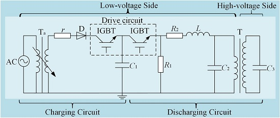
3. Loop Design of Switching Impulse Generator Based on Transformer Induction

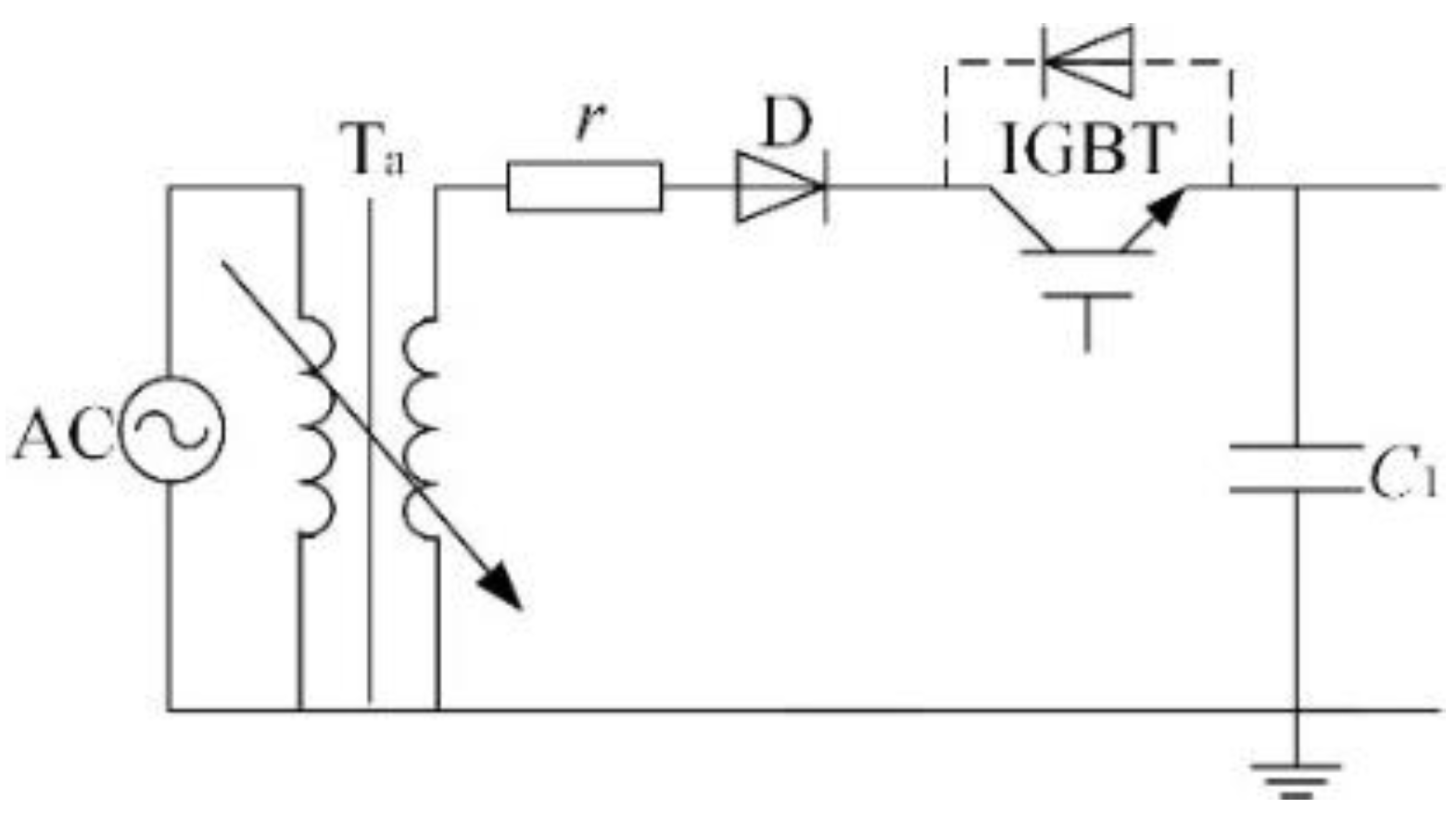
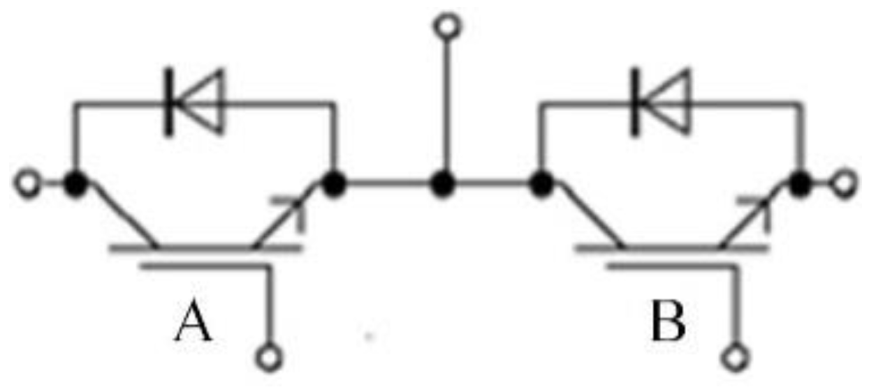
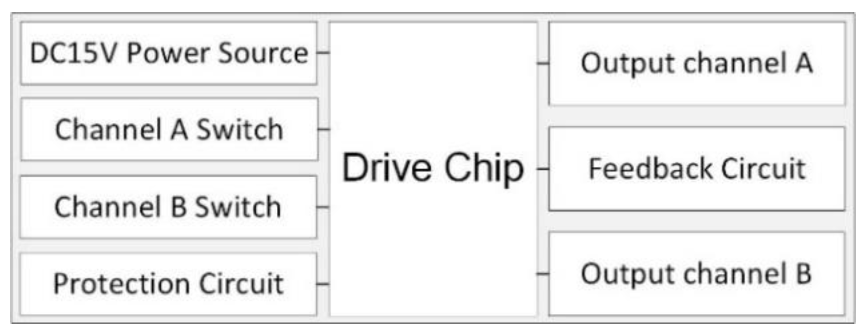
3.1. Insulated Gate Bipolar Transistor Module and Its Drive Circuit

3.1.1. Insulated Gate Bipolar Transistor Module

IGBT acts as a trigger-discharge switch. In the SI voltage generating circuit, the IGBT must withstand the voltage on the primary capacitor before discharge, and the maximum voltage must not exceed the peak voltage of the primary side. Additionally, the switching speed of the IGBT must be sufficiently fast, and its on-off time should be very much lesser than the peak time of the SI voltage. Figure 11 shows that the selected IGBT module in this study is Model FF100R12RT4 (IGBT Module, Infineon, Neubiberg, Germany), which consists of two IGBTs in series and each IGBT has an anti-parallel diode to follow the current and for protection.

3.1.2. Drive Circuit of Insulated Gate Bipolar Transistor

The main function of the IGBT drive circuit is to isolate the control and main circuits. According to the demand, the circuit should not only correctly control the on-off of the IGBT but also provide a certain protection function. In particular, it is supposed to shut off the IGBT when it suffers from overcurrent or overvoltage.
This study designs an IGBT drive circuit, and the schematic diagram is shown in Figure 12. The entire drive circuit consists of a 15 V direct current (DC) power source, channels A and B switches, output channels A and B, a feedback circuit, and a protection circuit. Here, the IGBT drive circuit is powered by the 15 V DC power source. Channels A and B respectively correspond to the left and right IGBTs shown in Figure 11. When the channel switch is closed, the corresponding IGBT tube conducts. According to the design purpose, when the channel A switch is closed and the channel B switch is opened, the left side IGBT tube in Figure 11 conducts, and the power supply begins to charge main capacitor C1. After the charging is completed, the channel A switch is disconnected. Next, the channel B switch is closed, and the right side IGBT tube conducts. Then, the main capacitor C1 starts discharging to the primary winding of the transformer. Finally, the secondary side of the transformer induces the desired SI voltage. The output feedback module is mainly used to monitor whether the driver circuit properly works. If abnormal, the driver chip is reset by the protection circuit to protect the driver chip and the IGBT module. Moreover, the driver chip, which mainly completes the control and operation function of the drive circuit, is the core of the entire drive circuit.

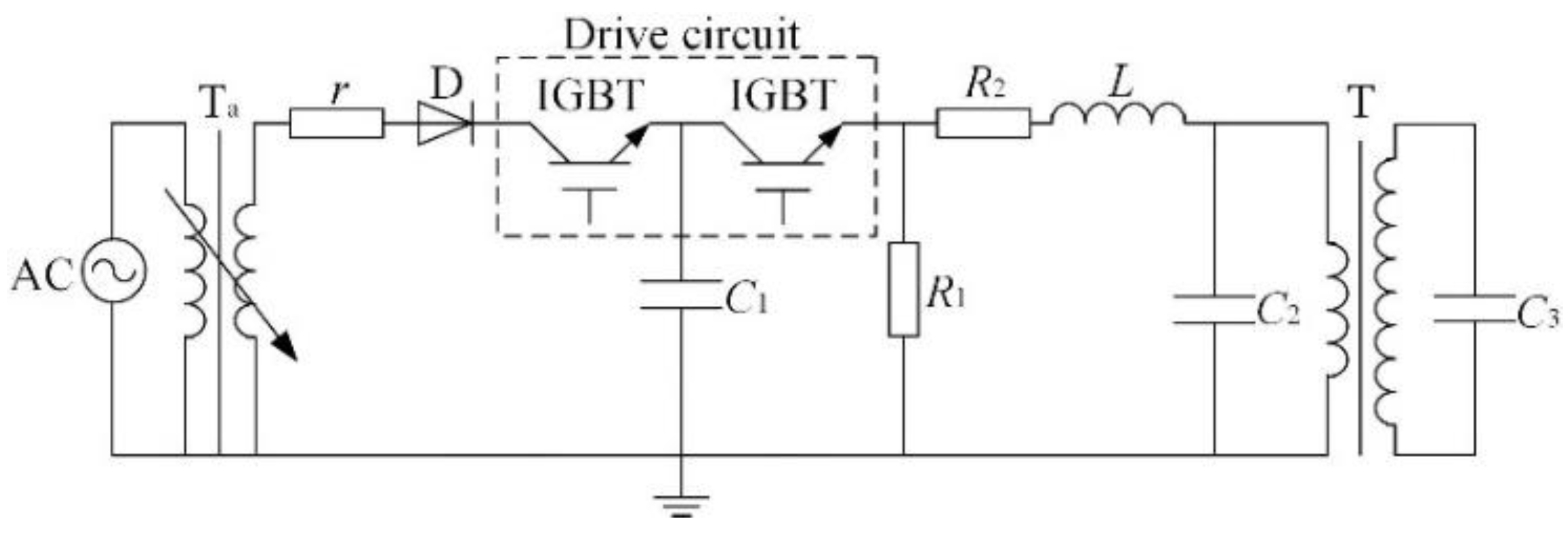
3.2. Design of the Main Circuit

3.2.1. Charging Circuit

Because the collector–emitter of the IGBT cannot withstand a negative voltage, it should be connected in series with a diode, which blocks the reverse voltage, or a rectifier. Further, the charging circuits also need a large series resistance r as a current-limiting resistor. However, it extends the charging time of the circuit. The diagram of the charging circuit is shown in Figure 13.
Changing the polarity of the output can be achieved by reversing the connections of diode D and the IGBT. After the IGBT is turned on, main capacitor C1 can be fully charged within 3–5 time constants (T = rC1). Before the discharge is triggered, the IGBT should be shut off to ensure that the discharge circuit is isolated from the power supply. The value of the withstand voltage of diode D must be greater than the maximum peak of the output from the power supply, and its through-current capability should exceed the value ωC1Um. To determine the value of r, both the maximum current limited by the IGBT parameter and the charging time determined by C1 should be taken into consideration.

3.2.2. General Circuit

Figure 14 shows the general circuit to generate the SI voltage. The two IGBT module tubes are connected in series and used as switches for the charging and discharging circuits. Secondary voltage of Ta must be matched with the primary voltage of T, i.e., the maximum output of Ta should be greater than the maximum input of T. Considering circuit efficiency, C1 should be determined by C3, which is the equivalent capacitance of T or the test sample. Converted into the primary side of T, C3 and C2 can be combined into C2'. Thus, IMR can be estimated by Equation (11):
I M R k · C 1 C 1 + C 2 · R 1 R 1 + R 2

4. Experimental Results

Based on the earlier theoretical discussion, each test was implemented according to the following procedures:
i 
Determine the target impulse waveform parameters, such as output voltage, rise time, half peak time and oscillating frequency;
ii 
Define the immutable parameters of the circuit component, such as charging capacitor and transformer;
iii 
Run S-IMR diagram for parameter optimization;
iv 
Adjust the component according to the calculated parameters;
v 
Make a comparison between the actual output and the target impulse waveform.
The voltage waveforms were recorded by a digital oscilloscope (WaveSurfer 64Xs-B, LeCroy, New York, NY, USA) and a high voltage probe (P6015, Tektronix, Beaverton, OR, USA) which is in parallel connection with C3. Further, the IMR and error sources between the actual and theoretical waveforms are analyzed in this section.

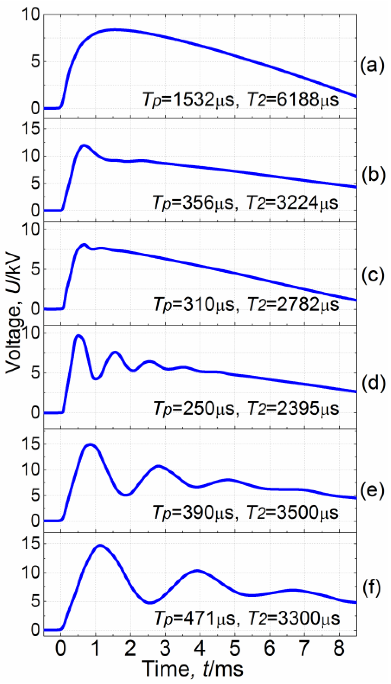
4.1. Experimental Results and Analysis

In the test, a 200 V/50 kV transformer, designated as T, is used, and Lm = 0.8455 H. The leakage inductance is 1.55 mH, which needs to be included in L during the numerical calculation. The value of the total capacitance in parallel with the secondary side of T is 500 pF. In practice, we should minimize the number of the components that need to be adjusted to promote efficiency and cost savings. In our test, all the parameters of the components in the primary side circuit were kept unchanged except for R2, C2 and L. Actually, the impulse voltage waveform can be effectively changed by adjusting R2, C2 and L.
Figure 15b–d shows the actual waveforms under different circuit parameter combinations. In the presence of leakage inductance with the order of millihenries, OSI waveform can be generated without L but with small damping resistance R2. The decrease of the damping resistance and increase of L will lead to more intense oscillation of the waveform and larger IMR. Decreasing wave-tail resistor R1 can significantly reduce T2 within a limited range, but T2 will not be endlessly increased by the increase in R1, i.e., as R1 increases, T2 will tend to saturate. If the load capacitance C3 is converted to the primary circuit by multiplying it with the transformer ratio, the value of equivalent capacitance C2’ would become very large. Therefore, an insufficient value of C1 would limit the amplitude of the output impulse and lengthen Tp. The comparison of the actual and calculated waveform parameters are listed in Table 3. It reveals that the influence of each component parameter of the voltage waveform is the same as that in the foregoing theoretical analysis.
It is worth noting that by using the IGBT, the impulse voltages are smoothly produced. The high-frequency oscillation that overlapped on the impulse waveform, which is attributed to the jitter of the traditional spark gap, does not exist in the IGBT-triggered impulses.

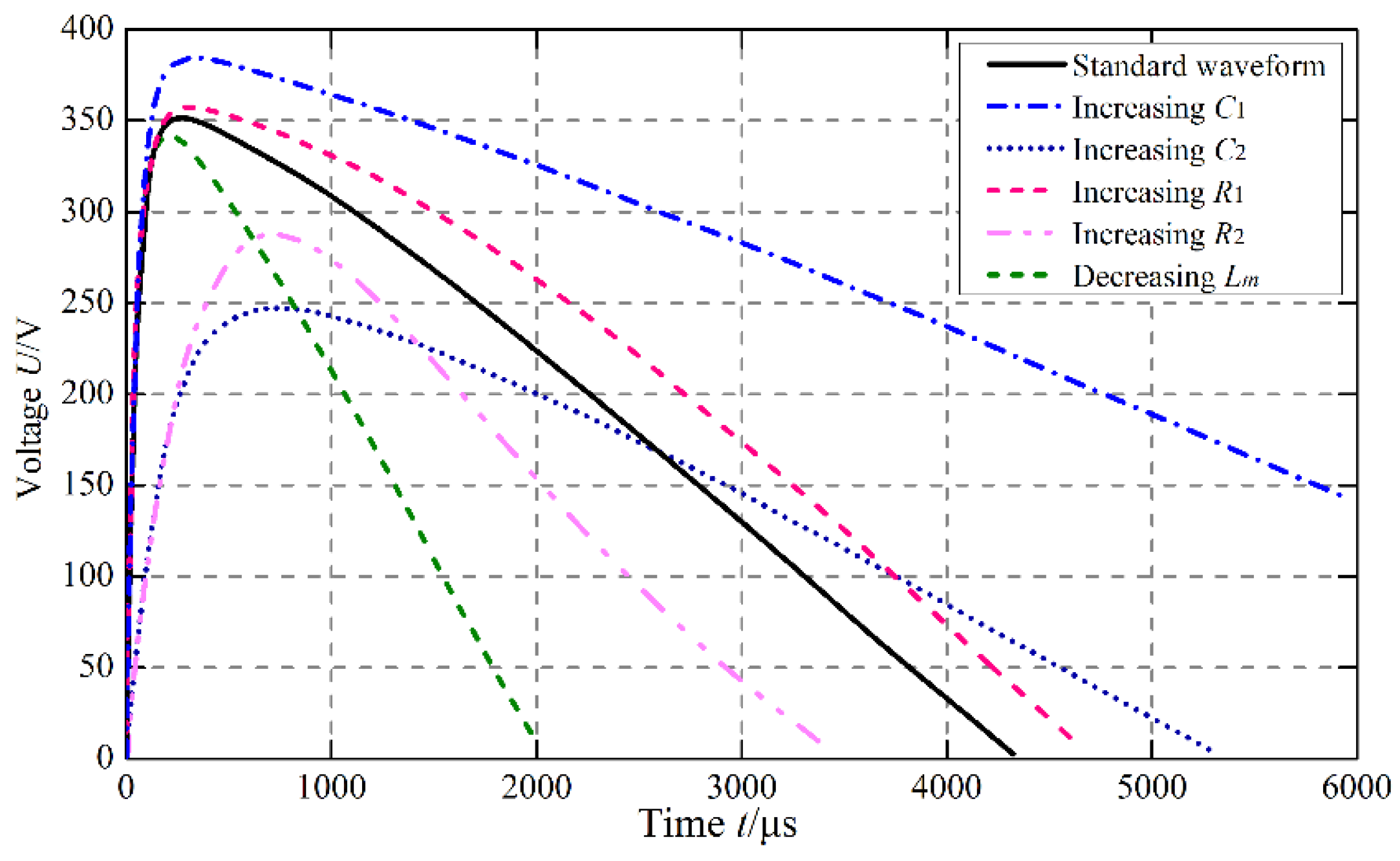
4.2. Control of Impulse Magnification Ratio

As analyzed earlier, increasing L or decreasing R2 can relatively improve IMR in a limited range. Additionally, if the variation in the time parameters of the waveforms (Tp and T2) is permitted in a certain range, C1 should be chosen to be as large as possible to enhance the circuit efficiency and IMR. In general, the time parameters and IMR are considered to be a contradictory pair during the adjustment of the waveform and output level. However, our theoretical analysis indicates that decreasing the leakage inductance (Lm) and the equivalent capacitance (part of C3) of the transformer can effectively reduce waveform parameters Tp and T2, which may provide an effective solution to the contradiction. In other words, if the leakage inductance, winding resistance, and equivalent capacitance of the transformer are sufficiently small, waveform oscillation would be easier to produce, and the oscillation frequency would be higher; thus, Tp would be smaller. Therefore, choosing a transformer with small leakage inductance, winding resistance, and equivalent capacitance is necessary.

4.3. Error Sources

Table 3 indicates that the main differences between the parameters of the actual and calculated waveforms are Tp and T2. The results of smaller Tp in most cases are caused by the underestimation of the leakage inductance of the transformer. T2 is also generally smaller than T2' when T2 is relatively small, which may be because the resistance of the magnetizing branch of the transformer is ignored in the calculation.
Generally, the theoretical and practical studies on the technology based on IGBT triggering control and transformer induction proved that generating different types of SI voltage is possible, including SI and OSI recommended by the IEC60060-3 standard [4]. Furthermore, the waveform parameters to output a SI voltage can be easily adjusted by changing the parameters of the primaryside circuit elements.

5. Discussion

5.1. Technical Requirements in Achieving a Higher Amplitude and Larger Capacity Output Voltage

As stated earlier, to achieve higher voltage and larger capacity output of the SI voltage, two methods can be considered. One is that using a voltage doubling circuit or improving the output voltage of the voltage regulator enhances the voltage of the transformer primary side. In this case, the IGBT module is required not only to withstand the working voltage with higher amplitude for a long time but also to have a bigger energy discharge capability. The other is choosing a transformer with a greater transformation ratio. Under the circumstances, the intrinsic parameters of the transformer will also increase with the increase in the transformation ratio, which causes the output waveform to accordingly change. At this time, a T-type equivalent circuit of the transformer should be considered, instead of the Γ-type equivalent circuit. Thus, more accurate numerical analysis result of the output waveform can be obtained.

5.2. Technical Requirements in Achieving Lightning and Oscillating Lightning Impulse Voltage

By the same principle utilized in this paper, lightning impulse voltage can also be realized technically. However, the following technical issues need to be considered.
(1)
Because the peak time of the lightning impulse voltage is much smaller than that of the SI voltage, a faster switch response speed of the IGBT module is correspondingly required.
(2)
The single phase transformer, which is used to generate the lightning impulse voltage, needs to withstand the impulse voltage with a much shorter rise time. Thus, the transformer must guarantee sufficient insulating strength against damage under high impulse work condition, which is a necessary technical premise to output a lightning impulse voltage without failure.
(3)
With regard to lightning impulse voltage with smaller peak time and half-peak time, a tighter match among the circuit parameters (including the transformer parameters) should be ensured to achieve steady and controllable output. Due to the increase of the transformer working frequency, the Γ-type (or T-type) equivalent circuit of the transformer, which is originally applied to generate an SI voltage, cannot be effectively used to analyze the loop of the lightning impulse voltage. Thus, considering the winding capacitances and stray capacitances of transformer [15], a high-frequency equivalent circuit must be utilized (Figure 16). However, this model will certainly increase the complexity of the equivalent circuit of the entire system and makes the numerical analysis theory, which provides guidance in building the actual circuit, more difficult.

6. Conclusions

In this present paper, a new compact and removable SI generator based on transformer boosting was developed with IGBT control. An optimization design method was proposed by considering both of the output efficiency and waveform errors. By numerical calculation and error correction, the component parameters of the primary side of the transformer, such as the magnetic inductance, leakage inductance, winding resistance and equivalent capacitance, were determined for the target SIs. To address the synchronization problem which is usually caused by multiple spark gaps, an IGBT with drive circuit was employed as the impulse trigger. It was proven that the IGBT within the range of the forward withstand voltage can well replace the traditional sphere gap switch. The generator was finally built on a removable high voltage transformer with small size. The experiment showed that the waveform parameters of SI and OSI voltages generated by the new generator were consistent with the numerical calculation and the error estimation.

Acknowledgments

The authors would like to thank the project supported by the National Natural Science Foundation of China (Grant No. 51507130), China Postdoctoral Science Foundation (Grant No. 2014M560777), Special China Postdoctoral Science Foundation (Grant No. 2016-11-141158) and Shaanxi International Cooperation and Exchanges Foundation (Grant No. 2016KW-072).

Author Contributions

Ming Ren and Ming Dong conceived and designed the experiments; Rixin Ye performed the experiments; Chongxing Zhang analyzed the data and wrote the paper; Ricardo Albarracín gave some substantive suggestions and guidance for the research.

Conflicts of Interest

All authors declare that there is no conflict of interests regarding the publication of this paper.

References

  1. Neumann, C.; Rusek, B.; Balzer, G.; Jeromin, I.; Hille, C.; Schnettler, A. End of Life Estimation and Optimisation of Maintenance of HV Switchgear and GIS Substations; A3-201; Cigre: Paris, France, 2012. [Google Scholar]
  2. Al-Suhaily, M.; Meijer, S.; Smit, J.J.; Sibbald, P.; Kanters, J. Analysis of diagnostic methods to prevent failure of critical GIS components. In Proceedings of the 2010 International Conference on High Voltage Engineering and Application (ICHVE), New Orleans, LA, USA, 11–14 October 2010; pp. 220–223.
  3. Sabot, A.; Petit, A.; Taillebois, J.P. GIS insulation co-ordination: On-site tests and dielectric diagnostic techniques. A utility point of view. IEEE Trans. Power Deliv. 1996, 11, 1309–1316. [Google Scholar] [CrossRef]
  4. High Voltage Test Techniques—Part 3: Definitions and Requirements for On-Site Tests; IEC 60060-3; International Electrotechnical Commission: Geneva, Switzerland, 2006.
  5. Ren, M.; Dong, M.; Liu, Y.; Miao, J.; Qiu, A. Partial discharges in SF6 gas filled void under standard oscillating lightning and switching impulses in uniform and non-uniform background fields. IEEE Trans. Dielectr. Electr. Insul. 2014, 21, 138–148. [Google Scholar] [CrossRef]
  6. Li, J.; Zhang, L.; Liang, J.; Yao, X. Partial discharge characteristics over SF6/epoxy interfaces under impulse voltage. IEEE Trans. Dielectr. Electr. Insul. 2013, 20, 2158–2164. [Google Scholar] [CrossRef]
  7. Okabe, S.; Tsuboi, T.; Takami, J. Basic study of possible waveforms generated in lightning impulse withstand voltage test on UHV equipment. IEEE Trans. Dielectr. Electr. Insul. 2009, 16, 1127–1133. [Google Scholar] [CrossRef]
  8. Rozga, P. Streamer propagation and breakdown in a very small point-insulating plate gap in mineral oil and ester liquids at positive lightning impulse voltage. Energies 2016, 9, 467. [Google Scholar] [CrossRef]
  9. Siew, W.; Howat, S.; Chalmers, I. Radiated interference from a high voltage impulse generator. IEEE Trans. Electromagn. Compat. 1996, 38, 600–604. [Google Scholar] [CrossRef]
  10. Yan, Z.; Cui, X.; Su, S. Electromechanics; Xi’an Jiaotong University Press: Xi’an, China, 2006. [Google Scholar]
  11. Del Vecchio, R.M.; Ahuja, R.; Frenette, R.D. Determining ideal impulse generator settings from a generator-transformer circuit model. IEEE Trans. Power Deliv. 2002, 17, 142–148. [Google Scholar] [CrossRef]
  12. Ling, Y.; Chen, M. Calculation Method Tutorial; Xi’an Jiaotong University Press: Xi’an, China, 2005. [Google Scholar]
  13. Maffezzoni, P.; Codecasa, L.; D’Amore, D. Time-domain simulation of nonlinear circuits through implicit Runge-Kutta methods. IEEE Trans. Circuits Syst. I Regul. Pap. 2007, 54, 391–400. [Google Scholar] [CrossRef]
  14. Suzuki, C. Two-stage Sand-Runge-Kutta methods powerful for non-linear equations with multiple solutions. In Proceedings of the 2009 Computation World: Future Computing, Service Computation, Cognitive, Adaptive, Content, Patterns, Athens, Greece, 15–20 November 2009; pp. 575–579.
  15. Liu, X.; Wang, Y.; Zhu, J.; Guo, Y.; Lei, G.; Liu, C. Calculation of capacitance in high-frequency transformer windings. IEEE Trans. Magn. 2016, 52. [Google Scholar] [CrossRef]
Figure 1. Circuit diagram of the principle of generating switching impulse (SI). C1: Main charging capacitor; C2: wave-modulating capacitor; K: power electronic switch (insulated gate bipolar transistor (IGBT)); R1: wave-tail resistor; R2: wave-head resistor; L: wave-modulating inductor; T: transformer; and C3: load capacitor.
Energies 09 00644 g001
Figure 2. (a) T type; and (b) Γ type equivalent circuits of the transformer. L1: Leakage inductance of the low-voltage winding; L2: leakage inductance of the high-voltage winding; L: leakage inductance; R: winding resistance; R1, R2, Rm: winding resistance of the transformer; Lm: magnetizing inductance; Lm: magnetizing inductance of the transformer.
Energies 09 00644 g002
Figure 3. SI discharge equivalent circuit with IGBT.
Energies 09 00644 g003
Figure 4. Equivalent circuit during breakover of the IGBT. u1 and u2 are the potential differences of the capacitor. i1, i2, iL, iR1 are the current flows in this circuit.
Energies 09 00644 g004
Figure 5. Program flowchart to calculate the circuit parameters.
Energies 09 00644 g005
Figure 6. Subprogram flowchart of the waveform-parameter calculation.
Energies 09 00644 g006
Figure 7. Waveform error and impulse magnification ratio (S-IMR) diagram of the parameter optimization. The selected initial values are as follows: Lm = 0.9 H, C1 = 10 µF, R1 = 1155 Ω, C2 = 0.1 µF, and R2 = 10 Ω. The value ranges of C2 and R2 are (0.1, 2) µF and (10, 80) Ω, respectively. The step lengths of these two parameters are 0.1 µF and 1 Ω, respectively. The red point in Area III in Figure 7 is selected as: S = 0, IMR = 0.88, R2 = 56 Ω and C2 = 1 µF.
Energies 09 00644 g007
Figure 8. Simulated waveforms of SI voltage.
Energies 09 00644 g008
Figure 9. Oscillating switching impulse (OSI) waveform.
Energies 09 00644 g009
Figure 10. OSI waveform after changing L.
Energies 09 00644 g010
Figure 11. Diagram of the IGBT module principle.
Energies 09 00644 g011
Figure 12. Schematic diagram of the IGBT drive circuit.
Energies 09 00644 g012
Figure 13. Diagram of the charging circuit. AC: alternating current.
Energies 09 00644 g013
Figure 14. General circuit to generate the SI voltage based on the transformer.
Energies 09 00644 g014
Figure 15. SI waveforms under different circuit parameters.
Energies 09 00644 g015
Figure 16. High-frequency equivalent circuit of transformer. Rs1: Winding resistance of the primary side; Rs2: winding resistance of the secondary side; Lk1: leakage inductance of the primary side; Lk2: leakage inductance of the secondary side; Cp: winding capacitance of the primary side; Cs: winding capacitance of the secondary side; and Cps1, Cps2: winding stray capacitance between the primary side and the secondary side.
Energies 09 00644 g016
Table 1. Waveform parameters of SI voltage and their corresponding circuit parameters.
No.C1 (μF)C2 (μF)R1 (Ω)R2 (Ω)Lm (H)Tp (μs)T2 (μs)Um (V)IMR
(1)1011155560.92502500351.60.879
(2)1011155560.22051193341.50.854
(3)5011155560.92984895384.10.960
(4)1051155560.97123344246.00.615
(5)10111,550560.92802939357.10.893
(6)10111553360.97242079286.70.717
Table 2. Waveform parameters of OSI voltage and their corresponding circuit parameters.
No.C1 (μF)C2 (μF)R1 (Ω)R2 (Ω)L (mH)Lm (H)Tp (μs)T2 (μs)f (Hz)Um (V)IMR
(1)30.222.23k331.21.350100010k555.01.388
(2)30.222.23k334.91.31008555.0k631.41.579
(3)100.222.23k331.21.35219669.6k582.11.455
(4)31.122.23k331.21.310816604.6k353.20.883
(5)30.222.23k331.20.55068410k555.01.388
(6)30.2222k331.21.350135610k558.01.395
(7)30.221M331.21.350140510k558.21.396
(8)30.221k331.21.35070110k553.51.384
(9)30.222.23k251.21.35086510k591.31.478
(10)30.222.23k1201.21.3771520-375.60.939
(11)30.222.23k1801.21.31571492-359.80.900
Table 3. Comparisons of the actual waveform parameters and the numerical results under different circuit parameters.
Subfigure No.Circuit ParametersCharging VoltagePeak TimeHalf-Peak TimeOutput Voltage AmplitudeOutput Efficiency
L (mH)C1 (μF)C2 (μF)C3 (pF)R1 (Ω)R2 (Ω)UC1 (V)Tp (μs)TP’ (μs)ep (%)T2 (μs)T2’ (μs)e2 (%)Um (kV)Um’ (kV)em (%)IMR
15a1.5510150013005616015321549−1.161886272−1.38.48.67−3.152.5
15b1.5510050030010170356359−0.8432243442−6.312.012.58−4.670.6
15c1.554.7050013025200310315−1.6278227062.88.168.4−2.940.8
15d1.554.7050010004190250251−0.40239523910.189.8410.5−6.351.8
15e2.96.80500100,0004200396401−1.235003657−4.315.015.7−4.575
15f4.026.8050010004200471470−0.2133003402−3.014.815.6−5.174
Note: Tp, T2 and Um represent the actual waveform parameters; Tp’, T2’ and Um’ represent the calculated waveform parameters; ep, e2 and em represent error between the actual and calculated waveform parameters.

