Article

Low-Temperature, Chemically Grown Titanium Oxide Thin Films with a High Hole Tunneling Rate for Si Solar Cells

1
Department of Electrical Engineering, National Chung Hsing University, Taichung 40227, Taiwan
2
Graduate Institute of Optoelectronic Engineering, National Chung Hsing University, Taichung 40227, Taiwan
3
Research Center for Sustainable Energy and Nanotechnology, National Chung Hsing University, Taichung 40227, Taiwan
4
Green Energy and Environment Research Laboratories, Industrial Technology Research Institute, Chutung 310, Taiwan
*
Author to whom correspondence should be addressed.
Energies 2016, 9(6), 402; https://doi.org/10.3390/en9060402
Submission received: 8 March 2016 / Revised: 16 May 2016 / Accepted: 19 May 2016 / Published: 25 May 2016
(This article belongs to the Special Issue Key Developments in Thin Film Solar Cells)

Abstract

:
In this paper, we propose a chemically grown titanium oxide (TiO2) on Si to form a heterojunction for photovoltaic devices. The chemically grown TiO2 does not block hole transport. Ultraviolet photoemission spectroscopy was used to study the band alignment. A substantial band offset at the TiO2/Si interface was observed. X-ray photoemission spectroscopy (XPS) revealed that the chemically grown TiO2 is oxygen-deficient and contains numerous gap states. A multiple-trap-assisted tunneling (TAT) model was used to explain the high hole injection rate. According to this model, the tunneling rate can be 105 orders of magnitude higher for holes passing through TiO2 than for flow through SiO2. With 24-nm-thick TiO2, a Si solar cell achieves a 33.2 mA/cm2 photocurrent on a planar substrate, with a 9.4% power conversion efficiency. Plan-view scanning electron microscopy images indicate that a moth-eye-like structure formed during TiO2 deposition. This structure enables light harvesting for a high photocurrent. The high photocurrent and ease of production of chemically grown TiO2 imply that it is a suitable candidate for future low-cost, high-efficiency solar cell applications.

Graphical Abstract

1. Introduction

Heterojunction solar cells have recently become leading candidates for high-efficiency cells with a considerably low production cost. Heterojunctions are widely used in optoelectronic devices such as light-emitting diodes (LEDs) [1,2,3,4], laser diodes [5,6], and photodiodes (PDs) [7,8,9] because they enable manipulating either hole or electron transport selectively by applying an appropriate band alignment. The specific band alignment can either increase carrier recombination in a LED or move photocarriers into appropriate contact in a PD. A solar cell, an energy harvesting device, is a type of PD. To achieve a high photocurrent, holes and electrons should arrive at a specific electrode properly. Therefore, several material systems have been proposed and demonstrated to achieve appropriate heterojunctions in Si solar cells. Amorphous Si is a well-known material system deposited on crystalline Si to construct a heterojunction for high-efficiency solar cells by setting front and back surface fields [10]. A very thin (5–10 nm) intrinsic amorphous Si (a-Si:H) layer and a heavily p-type-doped amorphous Si (p-a-Si:H) layer were deposited sequentially through plasma-enhanced chemical vapor deposition (PECVD). The purpose of the intrinsic a-Si:H is to passivate the Si surface with hydrogen to prevent carrier recombination. However, this is a challenging process because PECVD involves ionic radicals that might damage the Si surface rather than passivate it. Although the a-Si:H-based heterojunction with intrinsic thin-film technology has demonstrated high efficiency, an alternative material that inherently exhibits excellent surface passivation and proper band alignment is required. Therefore, in addition to a-Si:H, metal oxides such as AlOx [11,12,13], SiO2 [14,15], and TiO2 [16,17] have been used in constructing carrier selective barriers with passivation ability on crystalline Si to achieve a high photocurrent. Pudasaini et al. [11] used ultrathin aluminum oxide (approximately 1.84 nm), grown through an atomic layer deposition, on an n-type Si wafer as a passivation layer in a poly(3,4-ethylenedioxythiophene) polystyrene sulfonate/Si hybrid heterojunction solar cell system. Sheng et al. [14] used a wet method to form silicon oxide on a Si wafer as a passivation layer. A 10.48% efficiency was achieved in a hybrid solar cell. Avasthi et al. [16] used low temperature chemical vapor deposition (CVD)-grown TiO2 (3 nm) on a p-type wafer to block holes, thereby achieving a 7.02% photoelectric conversion efficiency. Among the aforementioned materials, TiO2 is the most attractive because it exhibits a smaller bandgap that ensures efficient carrier tunneling. Furthermore, TiO2 was demonstrated to be an alternative to silicon nitride as a Si surface passivation layer [18]. However, CVD is a slow and expensive process that might limit productivity in the future. Moreover, n-type Si is preferred to p-type Si in solar cells because electrons move faster than holes do. Therefore, chemically depositing TiO2 at a low temperature is proposed for attaining a high hole tunneling rate on an n-type Si substrate for heterojunction solar cells.

2. Experimental

An n-type, surface polished (100) Si wafer (1–10 Ω-cm) 525 μm in thickness was diced into tiles with areas of 2 × 2 cm2 and used as the substrate. Prior to deposition, the Si substrate was cleaned chemically in a solution with an HF:H2O ratio of 1:10 for 30 s and then rinsed in deionized water. After the substrate was cleaned, a layer of TiO2 24–48 nm in thickness was deposited through liquid phase deposition (LPD). The deposition system consisted of:
(1)
an environment that was temperature controlled at an accuracy of ±0.1 °C;
(2)
a Teflon vessel containing the deposition solution.
To form the deposition solution, (NH4)2TiF6 and H3BO3 were dissolved in deionized water at concentrations of 0.2 M and 0.6 M, respectively. To deposit TiO2, this solution was saturated with TiO2 powder. The deposition temperature was maintained at 40 °C.
The mechanism for chemically growing TiO2 consists of two equilibrium reactions. The first is ligand exchange between metal-fluoro-complex ions (Equation (1)), and the second is an F ion consuming reaction in which boric acid serves as an F scavenger (Equation (2)) [19].
[TiF6]2− + nH2O ↔ [TiF6−n(OH)n]2− + nHF
H3BO3 + 4HF ↔ HBF4 + 3H2O
H3BO3 reacts readily with F to form stable BF4 ions, thereby promoting the consumption of uncoordinated F ions. TiO2 dissolves in the solution and reacts with (NH4)2TiF6 to produce a TiO2 film on the Si and HF in the solution. The formation of HF prohibits the growth of TiO2. At this moment, the H3BO3 consumes HF, thereby sustaining the growth of TiO2. The grown TiO2 was then rinsed in deionized water and was air-dried with purified nitrogen. After TiO2 deposition, a thin layer of B-doped a-Si:H (20 nm) was deposited through PECVD (13.56 MHz). A transparent conductor, indium–tin oxide (ITO), was then deposited through sputtering in a 80-nm-thick layer. Subsequently, front and back contacts, namely Ag (100 nm) and Al (200 nm), respectively, were deposited using a thermal evaporator. The dark current density-voltage characteristics of the fabricated solar cells were measured using an Agilent B2912A semiconductor parameter analyzer, and the photovoltaic characteristics were measured using the same setup equipped with a calibrated solar simulator under an air mass (AM) 1.5 G (100 mW/cm2) condition. The external quantum efficiency (EQE) was measured using a Titan Electro-Optics QE-3000 system (Titan Electro-Optics Co., Taipei, Taiwan). Scanning electron microscopy (SEM) images were taken using a JEOL JSM-6700F (JEOL USA Inc., Peabody, MA, USA). Transmission electron microscopy (TEM) measurements were obtained using a JEOL JEM-2100F (JEOL USA Inc.). X-ray photoelectron spectroscopy (XPS) measurement was performed using a ULVAC-PHI PHI 5000 Versa Probe (Physical Electronics, Inc., Chanhassen, MN, USA).

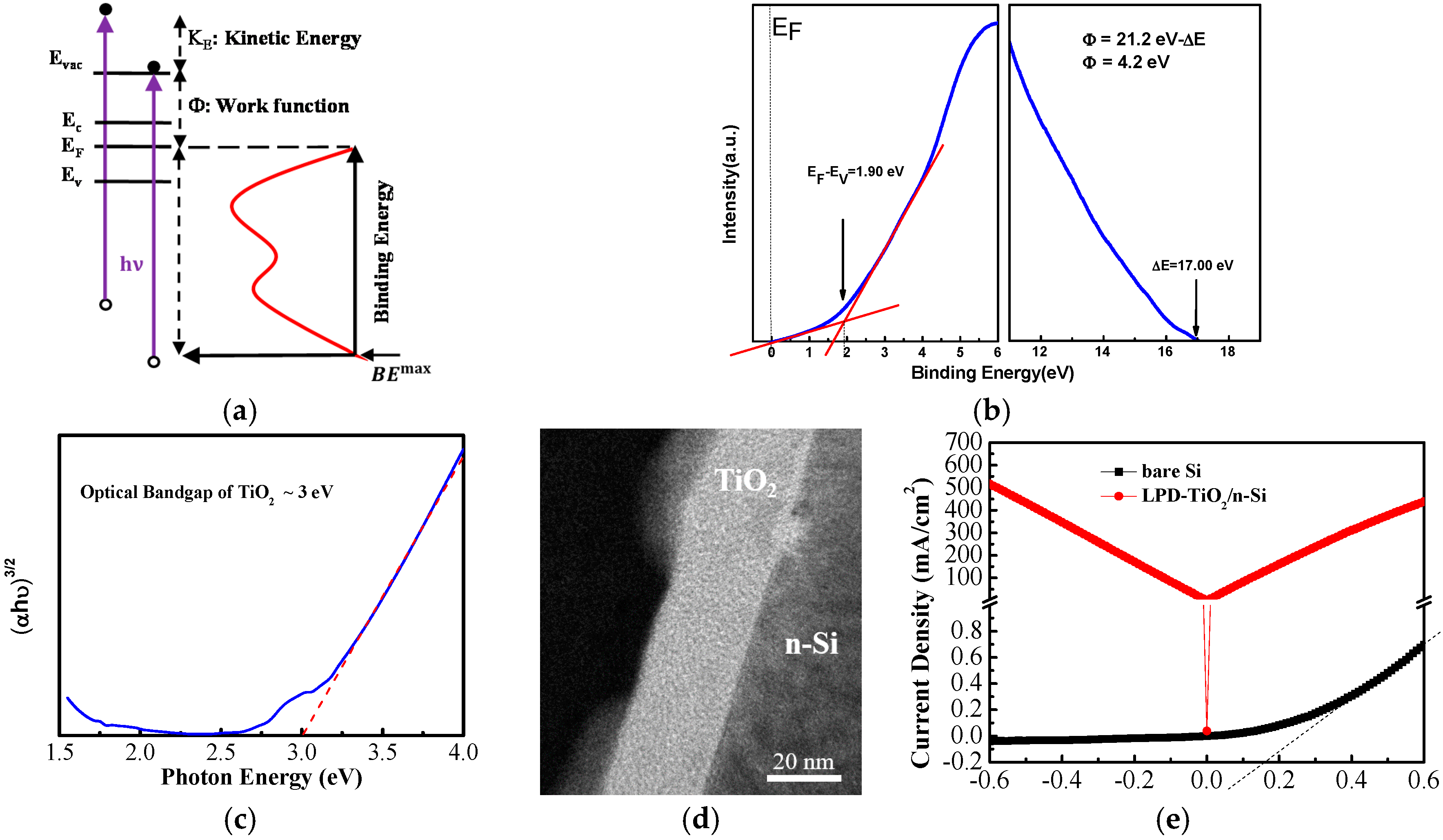
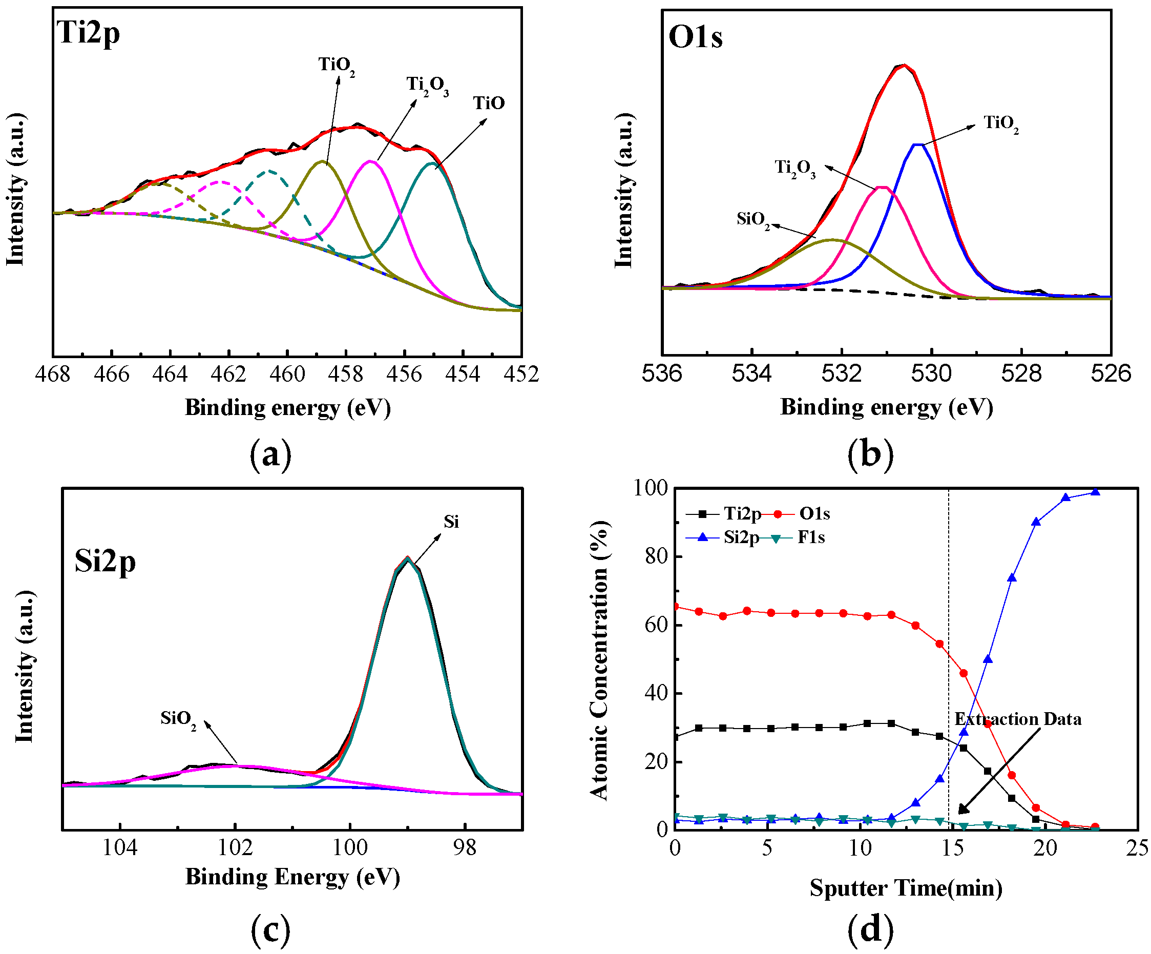
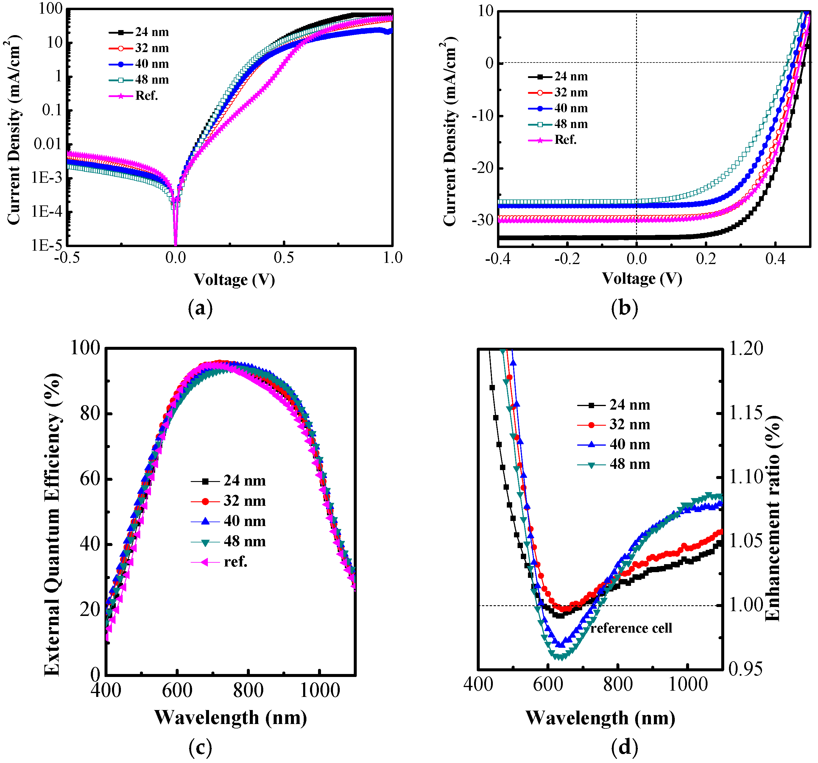
3. Results and Discussion

To determine the proper band alignment to n-type Si for carrier selection, ultraviolet (UV) photoemission spectroscopy (UPS) was performed to measure the energy levels of TiO2 [20]. The UPS was performed by emitting UV photons with an energy of 21.2 eV to the TiO2 film. The binding energy (BE) of photoelectrons was analyzed. A schematic of the mechanism is plotted in Figure 1a.
The Fermi energy (EF) of the solution-processed TiO2 is suggested to have an energy level between the conduction band edge (EC) and the valence band edge (EV) of the TiO2. Upon UV light illumination, valence electrons are excited and escape from the associated atoms with a kinetic energy (KE) measured by a detector. Therefore, the energy relationship of the system can be described by BE = hυ − KE − Φ, in which BE is the binding energy of an electron, determined as the difference between the energy of the electron in the valence band and the EF; hυ is the energy of the UV light; and Φ is the work function of the system, determined as the energy difference between the vacuum level and the EF. Therefore, a BE was obtained at each KE. The maximum BE was obtained at zero KE, as shown in Figure 1b. The work function (Ф) of the films was defined by Ф = hυ − ∆E, in which ∆E is determined as the BE at the cutoff edge of electron emission [20,21]. Extrapolation shows that the cutoff edge is 17 eV. Therefore, the work function is 4.2 eV in the LPD-grown TiO2 film. The energy difference between EF and EV can be determined at the rising point of electron emission through extrapolation, because the electrons are occupied mostly in the valence band in a semiconductor. The calculated EFEV difference is 1.9 eV. Accordingly, the EV is 6.1 eV below the vacuum level. The transmission spectrum of TiO2-grown glass was used to calculate the bandgap (Eg) of the TiO2 through the following procedure. The absorbance (A) of the TiO2 layer can be obtained using the relation A = 1 − RT, in which R is the reflectance, and T is the transmittance. With known thickness (d) and A, the absorption coefficient (α) can be deduced according to the relation A = exp(−αd). With the absorption coefficient, the optical bandgap of the TiO2 can be obtained according to a Tauc plot, as shown in Figure 1c. The optical bandgap of the TiO2 was determined to be 3 eV through this method. Accordingly, the EC is 3.1 eV from the vacuum level. In general, the EC and EV for Si are 4.05 eV and 5.17 eV, respectively. Therefore, the valence band barrier for the TiO2/Si interface is 0.93 eV.
A high-resolution TEM image of the grown TiO2 on crystalline Si is depicted in Figure 1d. The TiO2 layer is approximately 24-nm-thick. The TEM images confirm that the solution-processed TiO2 was smoothly deposited on the Si surface. To examine the ability of holes to tunnel through TiO2, an Al/TiO2/Si diode structure was used to measure the I-V characteristics, as shown in Figure 1e. The current density, as high as 100 mA/cm2, was obtained at a low voltage in the Al/TiO2/Si diode under both positive and negative biases, indicating that both electrons and holes can flow through the 24-nm-thick TiO2 efficiently without being blocked. The energy levels were measured through UPS as described. By contrast, without TiO2, Al/n-Si exhibits a Schottky diode behavior [15] with a Schottky barrier height of 0.157 eV, as shown in Figure 1e.
To identify the reason for the efficient hole tunneling, the chemical structure of TiO2 was explored through XPS. Figure 2a shows the atomic concentration depth profile for a thick TiO2 film. Clear Ti and Si intermixing at the surface is evident. To further study the interface, the BE spectra of Ti 2p, O 1s, and Si 2p signals at the interface were analyzed and are shown in Figure 2b–d, respectively. After deconvolution, the Ti 2p 2p3/2 spectra have three peaks, which are associated with TiO (454.7 eV), Ti2O3 (457 eV), and TiO2 (458.7 eV) [22], indicating that oxygen is deficient in the TiO2 film. The O1s spectra also have three peaks, which are associated with TiO2 (530.3 eV), oxygen-deficient TiO2 (531.1 eV), and SiO2 (532.2 eV) [22,23]. The oxygen deficiency implies the existence of Ti dangling bonds, which cause gap states in the LPD-TiO2 film. These gap states stimulate trap-assisted tunneling (TAT), which ensures that the photogenerated holes in Si are transported through the TiO2 to the ITO anode. The Si2p spectra have two peaks, which are associated with Si (99 eV) and Si–O (102 eV) [23,24]. The presence of Si–O bonding indicates that small amounts of SiO2 exist inside the TiO2 or at the Si surface. The incorporation of Si is an essential property of LPD-grown TiO2 film. The Si dissolves into the solution through HF etching during LPD of TiO2. The dissolved Si then forms either Ti–O–Si or Si–O bonds at the TiO2/Si interface. The coexistence of oxygen-deficient Ti and Si bonding and oxygen-bridging Ti and Si bonding may be responsible for the reduction of the measured barrier height for holes between Si and LPD-TiO2.
Figure 3a shows a schematic of band alignment in a fabricated heterojunction solar cell based on UPS measurement. According to the band alignment, the photogenerated electrons and holes are transported to the cathode and anode, respectively, by the established electrical field. The holes are probably blocked by barriers set by the TiO2. However, the experimental observations indicated that holes can flow through such barriers, as shown in Figure 1d. A mechanism of TAT through the gap states in TiO2 was proposed to be responsible for the high tunneling rate of holes. The physical theorem and calculation relevant to TAT have been discussed [25,26,27,28,29]. A multiple trap center model was used to simulate the tunneling current in the SiO2. The current density attained through multiple-TAT was calculated to be approximately 8 orders of magnitude higher than the current density achieved through direct tunneling for 4.5-nm-thick SiO2. In addition, the multiple-TAT current gradually decreases as the SiO2 thickness increases. The carrier behavior in the valence band around TiO2 based on this model is illustrated in Figure 3b.
When holes become close to TiO2, they are captured by traps (gap states) and then emitted to a-Si:H by the internal field. Therefore, the capture rate (Rci) and emission rate (Rei)) are dominant factors influencing the tunneling current. The current density can be expressed as the sum of the capture and emission rates Ri in each trap multiplied by the trap cross section Δ χ i , as shown in Equation (3).
J = q i R i Δ χ i  
Under a high internal field, the carriers must tunnel through the TiO2, and the emission rate must be higher or equal to the capture rate. Therefore, the calculation focuses on the emission rate. The emission rate can be expressed as the emission lifetime multiplied by the density of gap states, as shown in Equation (4). Furthermore, the emission lifetime can also be expressed by the relationship between the carrier distribution probability and the effective mass and energy levels, as shown in Equation (5). Finally, the tunneling current can be expressed by Equations (3) and (4) as expressed in Equation (6).
R ei τ ei 1 × N ti 1 ( m diel ) 2 × E T × E g exp [ ( E E T ) ] × N ti  
τ ei 1   1 ( m diel ) 2 × E T × E g exp [ ( E E T ) ]  
J 1 ( m diel ) 2 × E T × E g exp [ ( E E T ) ] × N ti × 1 m diel × E T  
In the preceding equations, mdiel is the effective hole mass (approximately 0.71 m0) in the dielectric, ET is the EV of TiO2, τ ei 1 is the emission lifetime, and Nti is the gap state concentration in the TiO2. On the basis of these equations, we can calculate the ratio of the tunneling current density in the TiO2 to that in the SiO2 at different gap state concentrations. In this calculation, the gap state density for SiO2 is fixed at 9 × 1017 cm3, as described in the literature [27]. This ratio is shown in Figure 3c. According to Figure 3c, at the same gap state density, the tunneling current through TiO2 is more than 100 times higher than that through SiO2. With an increase of the gap state density in the TiO2 to 1021 cm3, the tunneling current ratio becomes higher than 105. Such a high gap state density is reasonable. An oxygen-deficient signal was evident in XPS for TiO, and Ti2O3 occupied approximately two thirds of the Ti signal, whereas stoichiometric TiO2 occupied only approximately one third. Therefore, chemically grown TiO2 can withstand a high hole tunneling rate without blocking the holes.
The dark and photocurrent-voltage characteristics are illustrated in Figure 4a,b, respectively. All solar cells with a TiO2 layer ranging from 24 nm to 48 nm in thickness exhibit favorable junction behavior. The rectifier ratio calculated at 0.5 V is approximately 7500 for a device with 24-nm-thick TiO2. Other devices have similar values. The ideal factors for solar cells with 24-, 32-, 40-, and 48-nm-thick TiO2 layers are 1.63, 1.75, 1.71, and 1.45, respectively. Such moderate ideal factors indicate that carrier recombination is not high at the TiO2/Si interface. However, if the TiO2 layer is absent in the heterojunction solar cell, the reverse saturation current clearly increases. The reverse saturation current density, J0, for a reference device (without TiO2) is 7.12 × 10⁻⁷ A/cm2, and it is 3.54 × 10⁻⁷ A/cm2 for a device with 24-nm-thick TiO2. In addition, the reference device exhibits a relatively high ideal factor (>2) at a forward voltage. These findings indicate that TiO2 can properly passivate the interface between a-Si:H and Si as well as further improve the electrical contact behavior between them.
The photocurrent-voltage characteristics of heterojunction solar cells with and without TiO2, measured under an AM 1.5 G (100 mW/cm2) illumination condition by using a calibrated solar simulator, are illustrated in Figure 4b. The short-circuit current density (Jsc), open-circuit voltage (Voc), and fill factor for a heterojunction solar cell with TiO2 (24 nm) are 33.2 mA/cm2, 0.49 V, and 0.579, respectively, yielding a power conversion efficiency (PCE) of 9.42. By contrast, without a TiO2 interlayer, the values of those solar cell performance indicators are 29.9 mA/cm2, 0.47 V, and 0.586, yielding an 8.23% PCE. The enhanced performance is attributed to the properly aligned and passivated interfaces for hole tunneling between a-Si:H and Si achieved by inserting the TiO2 layer.
The Jsc is quite high for a planar solar cell containing no surface microstructure for light harvesting. As the thickness of TiO2 is increased to 48 nm, the Jsc decreases gradually to 26.3 mA/cm2. This implies that the PCE also gradually decreases, reaching 5.52% for a solar cell with 48-nm-thick TiO2. The details are listed in Table 1. This reduction is inversely proportional to the increase in the series resistance. Consequently, the reduction of the Jsc was attributed to slight current blocking by the thicker TiO2. The EQE of several fabricated solar cells is shown in Figure 4c. The solar cells with a TiO2 interlayer (24 nm and 32 nm) exhibit higher EQE than that of the solar cell without a TiO2 interlayer (reference) in both the short wavelength (400–580 nm) and near infrared (750–1100 nm) ranges. The enhanced EQE for the solar cells with a TiO2 interlayer indicates the probability of passivation at interfaces. It also indicates that the solar cells with a TiO2 interlayer may establish a higher internal electrical field than that of the reference cell inside the n-Si. Notably, the EQE of solar cells with thicker TiO2 interlayers (40 nm and 48 nm) is lower than that of the reference cell at 580–750 nm. This phenomenon is clearly explained by the enhancement ratio, which is expressed as the EQE of a solar cell with a TiO2 interlayer divided by the EQE of the reference cell. Figure 4d depicts the enhancement ratio for four samples; the EQE of solar cells with thicker TiO2 interlayers (40 nm and 48 nm) is 95% of the EQE of the reference cell. This may be attributed to slight carrier blocking by the TiO2. The calculated Jsc is listed in Table 1 and denoted by Jsc (EQE). The measured Jsc and Jsc (EQE) are highly similar for the reference sample. By contrast, the Jsc (EQE) for the solar cell with a 24-nm-thick TiO2 interlayer is lower than that of the measured Jsc. This may be due to the difference in the measurement setup between the solar simulator and the quantum efficiency spectrometer. However, the Jsc (EQE) also shows a decreasing trend as the TiO2 thickness increases, which is consistent with the proposed mechanism. The PCE based on Jsc (EQE) is also listed in Table 1.
The reduction in the barrier height and the ease of tunneling for carriers through the TiO2/Si interface can only ensure that the photocarrier is collected. They do not increase the light harvesting ability. To identify the reason for the high photocurrent (33.2 mA/cm2) obtained in the LPD-grown TiO2 heterojunction solar cell based on a polished Si substrate, the surface morphology of LPD-grown TiO2 on Si was characterized through SEM.
Figure 5a depicts plan-view SEM images of the LPD-grown TiO2 with different thicknesses. Many randomly arranged circular protrusions in a moth-eye-like structure were found over the LPD-TiO2 surface. The density of these structures increases as the TiO2 thickness increases. The diameter for each structure is approximately 100 nm. This dimension is close to the quarter wavelength of visible light in TiO2. Therefore, the interaction of incident light and LPD-grown TiO2 can be expressed by Mie scattering [30,31,32]. In the mechanism of Mie scattering, the percentage of back scattering is lower than that of Rayleigh scattering. Therefore, most of the incident light can be coupled into Si with high deflection. The deflected light can be reflected back and forth many times inside Si, increasing the absorbance of the incident light. This scattering mechanism is illustrated in Figure 5b. The reflectance of the LPD-grown TiO2 on Si at 300–800 nm is shown in Figure 5c. In the figure, thick TiO2 exhibits lower reflectance than that of thin TiO2, indicating that the incident light is more intense for the thick TiO2. However, the solar cell with the thick TiO2 exhibits a lower Jsc than that of the solar cell with the thin TiO2. Therefore, as the TiO2 thickness increases, hole transport through TiO2 to the anode becomes less easy, causing the current density to decrease. Consequently, the improved performance of the device is due to the enhanced hole transport rather than increased light trapping.

4. Conclusions

In conclusion, we demonstrated enhancements in Si-based heterojunction solar cells fabricated using a low temperature and liquid-phase-processed TiO2. LPD enables high throughput and low cost solar cell production. The LPD-TiO2 can passivate the Si surface, preventing plasma and chemical damage in subsequent processes. Through UPS investigation, the work function, EC, and EV for LPD-TiO2 were obtained. The band alignment indicates that electrons and holes could be collected properly. On the polished Si substrate, a 33.2-mA/cm2 short-circuit current was obtained. A moth-eye-like structure was observed on the LPD-grown TiO2 surface. Mie scattering in these structures ensures light harvesting and is responsible for the high photocurrent.

Acknowledgments

This work was financially supported by the Ministry of Science and Technology of Taiwan under MOST grant nos. MOST 104-2221-E-005-074.

Author Contributions

Yu-Tsu Lee and Zingway Pei conceived and designed the experiments; Fang-Ru Lin and Ting-Chun Lin performed the experiments; Yu-Tsu Lee and Zingway Pei analyzed the data; Chien-Hsun Chen contributed in a-Si:H deposition and efficiency measurement; Yu-Tsu Lee and Zingway Pei wrote the paper.

Conflicts of Interest

The authors declare no conflict of interest.

References

  1. Kang, H.; Kim, G.; Hwang, I.W.; Kim, Y.; Lee, K.C.; Park, S.H.; Lee, K. High-performance polymer tandem devices combining solar cell and light-emitting diode. Sol. Energy Mater. Sol. Cells 2012, 107, 148–153. [Google Scholar] [CrossRef]
  2. Morteani, A.C.; Dhoot, A.S.; Kim, J.S.; Silva, C.; Greenham, N.C.; Murphy, C.; Moons, E.; Cina, S.; Burroughes, J.H.; Friend, R.H. Barrier-free electron-hole capture in polymer blend heterojunction light-emitting diodes. Adv. Mater. 2003, 15, 1708–1712. [Google Scholar] [CrossRef]
  3. Chen, C.P.; Ke, M.Y.; Liu, C.C.; Chang, Y.J. Observation of 394 nm electroluminescence from low-temperature sputtered n-ZnO/SiO2 thin films on top of the p-GaN heterostructure. Appl. Phys. Lett. 2007, 91. [Google Scholar] [CrossRef]
  4. You, J.B.; Zhang, X.W.; Zhang, S.G.; Wang, J.X.; Yin, Z.G.; Tan, H.R.; Zhang, W.J.; Chu, P.K.; Cui, B.; Wowchak, A.M.; et al. Improved electroluminescence from n-ZnO/AlN/p-GaN heterojunction light-emitting diodes. Appl. Phys. Lett. 2010, 96. [Google Scholar] [CrossRef]
  5. Liang, H.K.; Yu, S.F.; Yang, H.Y. Directional and controllable edge-emitting ZnO ultraviolet random laser diodes. Appl. Phys. Lett. 2010, 96. [Google Scholar] [CrossRef]
  6. Zhu, H.; Shan, C.X.; Yao, B.; Li, B.H.; Zhang, J.Y.; Zhang, Z.Z.; Zhao, D.X.; Shen, D.Z.; Fan, X.W.; Lu, Y.M.; et al. Ultralow-threshold laser realized in zinc oxide. Adv. Mater. 2009, 21, 1613–1617. [Google Scholar] [CrossRef]
  7. Wang, D.Y.; Jiang, Y.T.; Lin, C.C.; Li, S.S.; Wang, Y.T.; Chen, C.C.; Chen, C.W. Solution-processable pyrite fes2 nanocrystals for the fabrication of heterojunction photodiodes with visible to NIR photodetection. Adv. Mater. 2012, 24, 3415–3420. [Google Scholar] [CrossRef] [PubMed]
  8. Shao, D.; Yu, M.; Lian, J.; Sawyer, S. Heterojunction photodiode fabricated from hydrogen treated ZnO nanowires grown on p-silicon substrate. Appl. Phys. Lett. 2012, 101. [Google Scholar] [CrossRef] [PubMed]
  9. Shao, D.; Yu, M.; Lian, J.; Sawyer, S. Heterojunction photodiode fabricated from multiwalled carbon nanotube/ZnO nanowire/p-silicon composite structure. Appl. Phys. Lett. 2013, 102. [Google Scholar] [CrossRef]
  10. Wolf, S.D.; Descoeudres, A.; Holman, Z.C.; Ballif, C. High-efficiency silicon heterojunction solar cells: A review. Green 2012, 2, 7–24. [Google Scholar] [CrossRef]
  11. Pudasaini, P.R.; Zepeda, F.R.; Sharma, M.; Elam, D.; Ponce, A.; Ayon, A.A. High Efficiency Hybrid Silicon Nanopillar-Polymer Solar Cells. ACS Appl. Mater. Interfaces 2013, 5, 9620–9627. [Google Scholar] [CrossRef] [PubMed]
  12. Pudasaini, P.R.; Elam, D.; Ayon, A.A. Aluminum oxide passivated radial junction sub-micrometre pillar array textured silicon solar cells. J. Phys. D Appl. Phys. 2013, 46. [Google Scholar] [CrossRef]
  13. Pudasaini, P.R.; Sharma, M.; Zepeda, F.R.; Ayon, A.A. Efficiency improvement of a nanostructured polymer solar cell employing atomic layer deposited Al2O3 as a passivation layer. Microelectron. Eng. 2014, 119, 6–10. [Google Scholar] [CrossRef]
  14. Sheng, J.; Fan, K.; Wang, D.; Han, C.; Fang, J.; Gao, P.; Ye, J. Improvement of the SiOx passivation layer for high-efficiency Si/PEDOT:PSS heterojunction solar cells. Appl. Mater. Interfaces 2014, 6, 16027–16034. [Google Scholar] [CrossRef] [PubMed]
  15. Neamen, D.A. Semiconductor Physics and Devices, 4th ed.; McGraw-Hill: New York, NY, USA, 2012. [Google Scholar]
  16. Avasthi, S.; McClain, W.E.; Man, G.; Kahn, A.; Schwartz, J.; Sturm, J.C. Hole-blocking titanium-oxide/silicon heterojunction and its application to photovoltaics. Appl. Phys. Lett. 2013, 102. [Google Scholar] [CrossRef]
  17. Salim, T.; Yin, Z.; Sun, S.; Huang, X.; Zhang, H.; Lam, Y.M. Solution-processed nanocrystalline TiO2 buffer layer used for improving the performance of organic photovoltaics. ACS Appl. Mater. Interfaces 2011, 3, 1063–1067. [Google Scholar] [CrossRef] [PubMed]
  18. Richards, B.S.; Cotter, J.E.; Honsberg, C.B. Enhancing the surface passivation of TiO2 coated silicon wafers. Appl. Phys. Lett. 2002, 80. [Google Scholar] [CrossRef]
  19. Lee, M.K.; Lee, H.C.; Hsu, C.M. High dielectric constant TiO2 film grown on polysilicon by liquid phase deposition. Mater. Sci. Semicond. Process. 2007, 10, 61–67. [Google Scholar] [CrossRef]
  20. Li, C.Y.; Wen, T.C.; Lee, T.H.; Guo, T.F.; Huang, J.C.A.; Lind, Y.C.; Hsu, Y.J. An inverted polymer photovoltaic cell with increased air stability obtained by employing novel hole/electron collecting layers. J. Mater. Chem. 2009, 19, 1643–1647. [Google Scholar] [CrossRef]
  21. Ishii, H.; Sugiyama, K.; Ito, E.; Seki, K. Energy level alignment and interfacial electronic structures at organic/metal and organic/organic interfaces. Adv. Mater. 1999, 11, 605–625. [Google Scholar] [CrossRef]
  22. Fang, Q.; Meier, M.; Yu, J.J.; Wang, Z.M.; Zhang, J.Y.; Wu, J.X.; Kenyon, A.; Hoffmann, P.; Boyd, I.W. FTIR and XPS investigation of Er-doped SiO2–TiO2 films. Mater. Sci. Eng. B 2003, 105, 209–213. [Google Scholar] [CrossRef]
  23. Anandan, C.; Bera, P. XPS studies on the interaction of CeO2 with silicon in magnetron sputtered CeO2 thin films on Si and Si3N4 substrates. Appl. Surf. Sci. 2013, 283, 297–303. [Google Scholar] [CrossRef]
  24. Zhang, W.; Zhang, S.; Liu, Y.; Chen, T. Evolution of Si suboxides into Si nanocrystals during rapid thermal annealing as revealed by XPS and Raman studies. J. Cryst. Growth 2009, 311, 1296–1301. [Google Scholar] [CrossRef]
  25. Lee, W.C.; Hu, C. Modeling CMOS tunneling currents through ultrathin gate oxide due to conduction- and valence-band electron and hole tunneling. IEEE Trans. Electron Devices 2001, 48, 1366–1373. [Google Scholar]
  26. Yu, S.; Guan, X.; Wong, H.-S.P. Conduction mechanism of TiN/HfOx/Pt resistive switching memory: A trap-assisted-tunneling model. Appl. Phys. Lett. 2011, 99. [Google Scholar] [CrossRef]
  27. Entner, R.; Gehring, A.; Kosina, H.; Grasser, T.; Selberherr, S. Impact of multi-trap assisted tunneling on gate leakage of CMOS memory devices. NSTI Nanotech 2005, 3, 45–48. [Google Scholar]
  28. Vandelli, L.; Padovani, A.; Larcher, L.; Southwick, R.G.; Knowlton, W.B.; Bersuker, G. A Physical model of the temperature dependence of the current through SiO2/HfO2 stacks. IEEE Trans. Electron Devices 2011, 58, 2878–2887. [Google Scholar] [CrossRef]
  29. Gehring, A.; Selberherr, S. Modeling of Tunneling Current and Gate Dielectric Reliability for Nonvolatile Memory Devices. IEEE Trans. Electron Devices 2004, 4, 306–319. [Google Scholar] [CrossRef]
  30. Coenen, T.; Van de Groep, J.; Polman, A. Resonant modes of single silicon nanocavities excited by electron irradiation. ACS Nano 2013, 7, 1689–1698. [Google Scholar] [CrossRef] [PubMed]
  31. Spinelli, P.; Macco, B.; Verschuuren, M.A.; Kessels, W.M.M.; Polman, A. Al2O3/TiO2 nano-pattern antireflection coating with ultralow surface recombination. Appl. Phys. Lett. 2013, 102. [Google Scholar] [CrossRef]
  32. Brongersma, M.L.; Cui, Y.; Fan, S. Light management for photovoltaics using high-index nanostructures. Nat. Mater. 2014, 13, 451–460. [Google Scholar] [CrossRef] [PubMed]
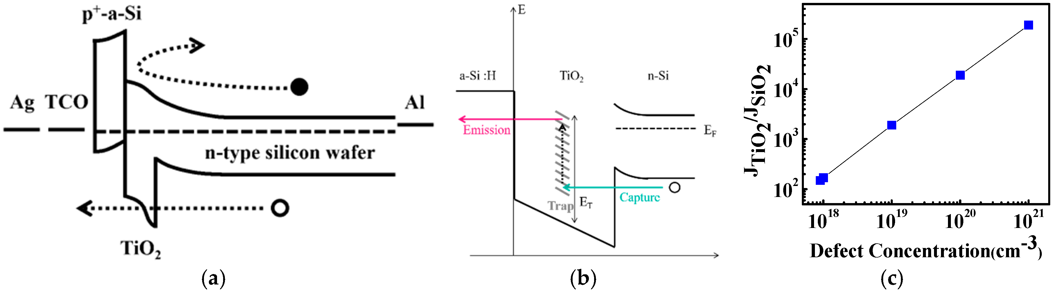
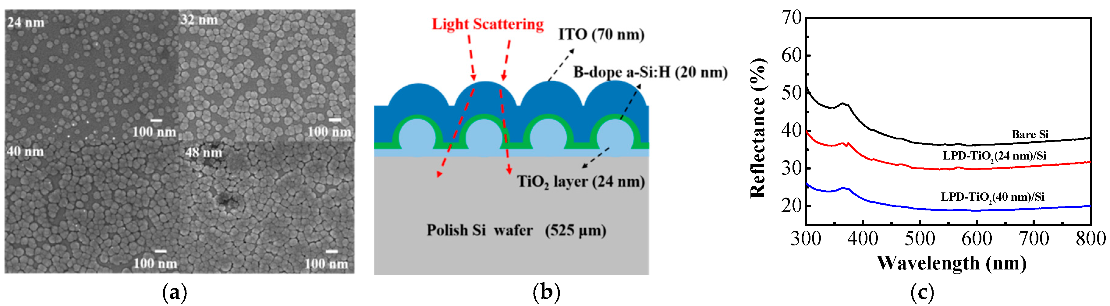
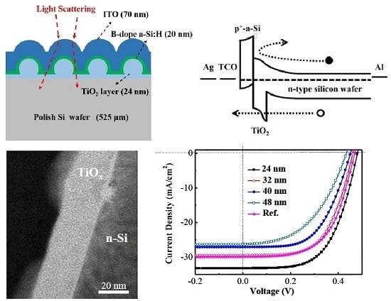
Figure 1. (a) Schematic of work function of TiO2 determined through ultraviolet (UV) photoemission spectroscopy (UPS) spectroscopy; (b) UPS spectrum of liquid phase deposition (LPD)-TiO2; (c) optical bandgap of TiO2 layer; (d) image of TiO2/Si interface taken through transmission electron microscopy (TEM); and (e) I-V characteristics of Al/LPD-TiO2/Si diode.
Energies 09 00402 g001
Figure 2. (a) Ti 2p; (b) O 1s; (c) Si 2p core level atomic structures for LPD-TiO2 obtained through X-ray photoelectron spectroscopy (XPS); and (d) depth profiles of these signals.
Energies 09 00402 g002
Figure 3. (a) Band alignment of proposed TiO2/Si heterojunction solar cell; (b) enlarged part of band diagram at EV around interface of TiO2/Si; and (c) ratio of tunneling current through TiO2 to that through SiO2 (JTiO2/JSiO2) according to gap state concentration.
Energies 09 00402 g003
Figure 4. Photocurrent-voltage characteristics for heterojunction solar cells containing TiO2 at different thicknesses: (a) dark I-V characteristics; (b) photocurrent-voltage characteristics obtained under AM 1.5G; (c) external quantum efficiency (EQE) of solar cells; and (d) ratio of EQE enhancement of solar cells with TiO2 interlayer relative to the reference cell.
Energies 09 00402 g004
Figure 5. (a) Plan-view scanning electron microscopy (SEM) images of LPD-TiO2 on Si; (b) proposed light scattering process in TiO2 solar cell. The inset of (c) shows the measured surface reflectance of planar Si and LPD-TiO2 on Si.
Energies 09 00402 g005
Table 1. Photovoltaic characteristics of TiO2/Si heterojunction solar cells.
ParameterRef. a24 nm32 nm40 nm48 nm
Voc (V)0.470.490.470.460.44
Jsc (mA/cm2)29.933.229.527.126.3
Jsc (EQE) (mA/cm2)30.531.7731.8831.4230.59
Fill Factor0.5860.5790.5830.5560.477
Efficiency (%)8.239.428.096.935.52
Efficiency EQE (%)8.409.018.737.986.42
Rs (Ω-cm2)3.833.54.445.35
Rsh (Ω-cm2)18551875172711,8755369
a p-a-Si:H/n-Si heterojunction solar cell.

