2.1. The In2Se3, Ga2Se3, and Cu System
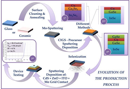
The CIGS solar cell fabrication starts with a direct current (DC) magnetron sputtering deposition in an argon atmosphere of amolybdenum back contact on a 4-mm-thick SLG substrate. Then, an In
2Se
3, Ga
2Se
3, and Cu sequence is deposited on top of the molybdenum film in the same sputtering chamber without breaking the vacuum [
6].
In particular, this process involves a radio frequency (RF) magnetron sputtering deposition of a 1000-nm-thick In
2Se
3 film at a substrate temperature of about 670 K, with 3.3 W/cm
2 power density at a deposition rate of 1 nm/s under a 0.5 Pa argon pressure (this deposition rate was measured with a quartz micro-balance, while film thickness was measured with a profilometer) [
7]. On top of the In
2Se
3 layer, a 330-nm-thick Ga
2Se
3 film is deposited by RF magnetron sputtering, at a substrate temperature of about 720 K, with a 1.8 W/cm
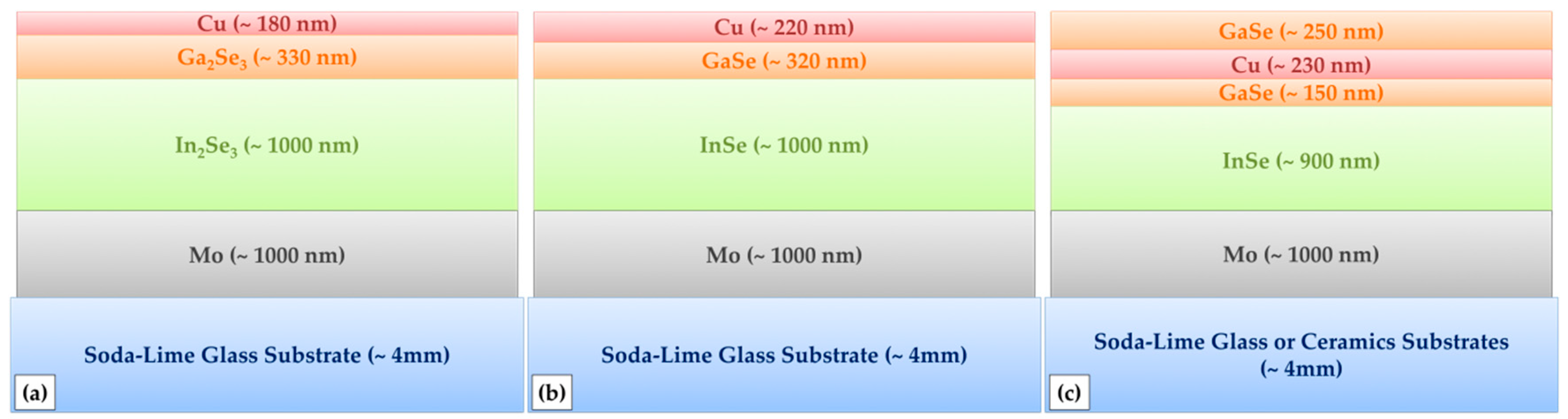
2 power density at a deposition rate of 0.4 nm/s under a 0.2 Pa argon pressure. Immediately after, a 180-nm-thick Cu film is deposited by d.c. magnetron sputtering, at a substrate temperature of about 620 K, with a 1.8 W/cm
2 power density at a deposition rate of 0.6 nm/s under a 0.2 Pa argon pressure (
Figure 1a). The difference between the deposition temperatures of these layers is due to the high reactivity and diffusivity of copper. Its diffusion increases as temperature rises. Cu reactivity is so strong that it induces surface segregation of secondary phases and partial separation of the crystalline grains, which negatively affect film uniformity. This problem can be avoided by depositing Cu on top of the Ga
2Se
3 film at low substrate temperature (≤620 K). By performing a further annealing in vacuum at a temperature of 670 K, a uniform film with enhanced single-phase crystallization is finally obtained. The compositional uniformity of the precursor material allows the selenization process, which is performed in a pure-selenium atmosphere for 10 min at a temperature of about 800 K.
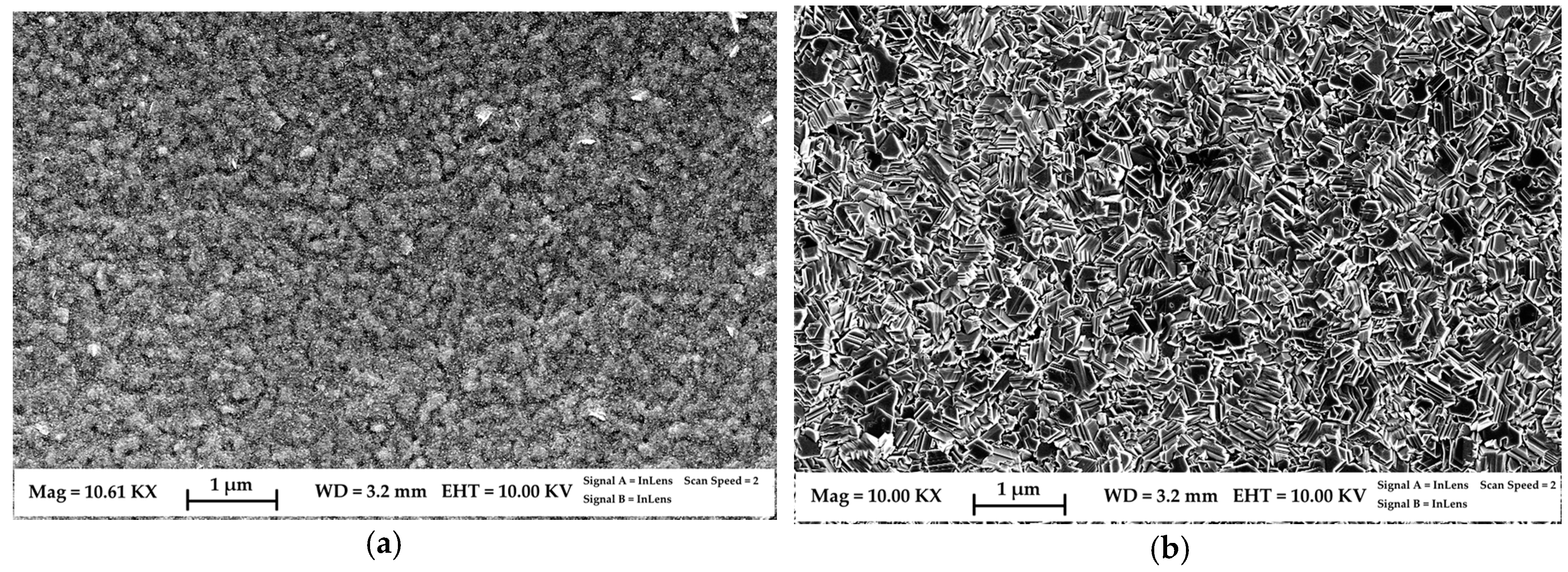
The CIGS absorber material prepared according to this method displays a uniform morphology throughout the whole substrate area, as can be seen in
Figure 2 and
Figure 3.
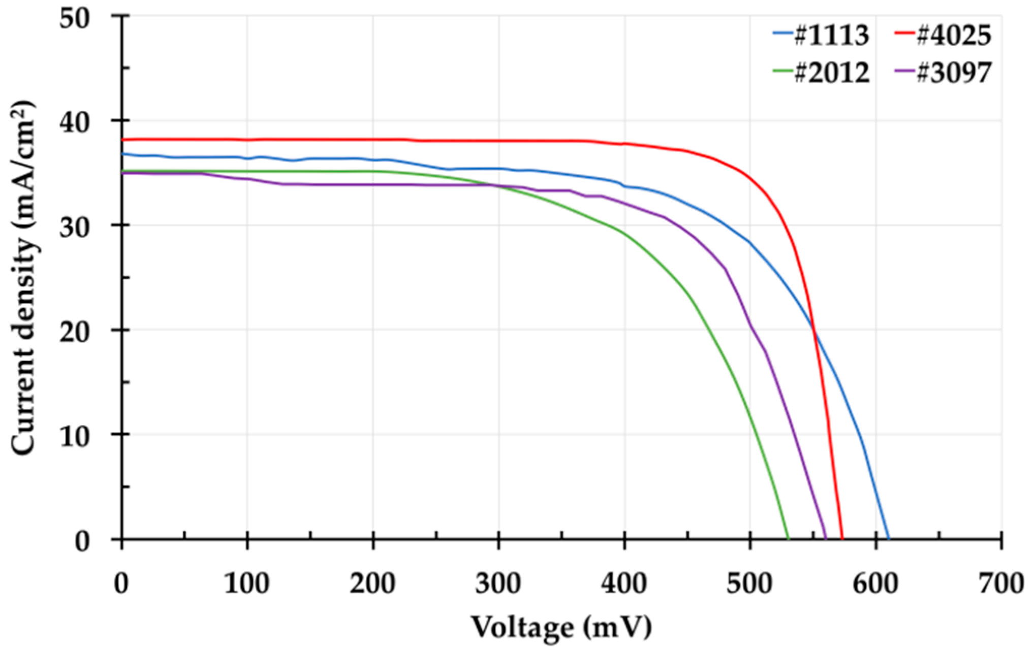
This material can be obtained with a similar morphology and composition even when a vacuum annealing is not performed before the selenization stage with the great benefit of a strong reduction in the process time. The highest photovoltaic parameters exhibited by solar cells produced with this absorber material are the following: open-circuit voltage V
OC = 530 mV, short-circuit current density J
SC = 35.16 mA/cm
2, fill-factor FF = 58%, and efficiency η = 10.81%. Measurements were performed at 298 K under 100 mW/cm
2 air mass (A.M.) 1.5 filtered light (standard conditions) (Current Density-Voltage (J-V) curve in
Figure A1, sample #2012). It is possible, in these thermodynamic conditions, that a CuInSe
2 (CIS) matrix with a more ideal crystal structure can form, preventing the lattice defects from trapping the photo-generated carriers and allowing them to be collected and transported more effectively through the junction.
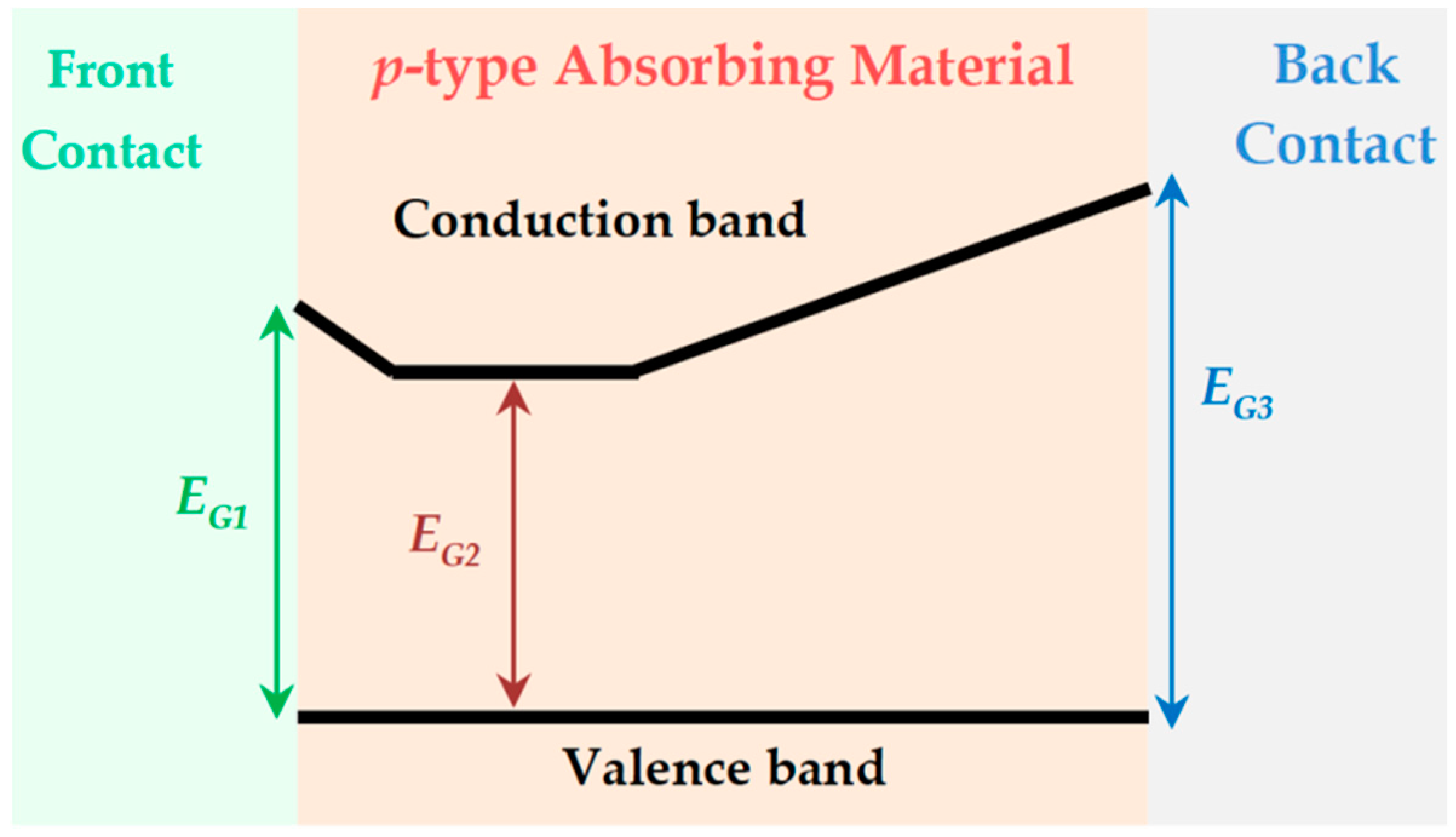
In order to obtain CIGS-based solar cells of higher efficiency, a proper distribution of a Ga concentration within the absorber material is needed. In particular, an accurately tailored double-graded Ga concentration may allow for the engineering of a specific energy gap (E
G) design (
Figure 4). If this design is followed, a back grading will provide an additional drift field for the minority electrons, and this will in turn improve carrier collection and reduce back-contact recombination [
8,
9,
10]. A second Ga grading will appear near the CIGS/CdS interface where the Ga concentration will be made higher towards the p-n junction. This superficial grading region must be kept thin enough, well below 20 nm, to let carriers overcome this barrier or pass through it by a tunnel mechanism. This makes it possible to increase the V
OC. In order to increase, as much as possible, the amount of solar photons absorbed inside the space charge region, a low E
G layer has to be produced inside the absorber. This layer, with a thickness of about 1000 nm, can increase the long wavelength absorption and thus supply a higher amount of photo-generated carriers [
11,
12].
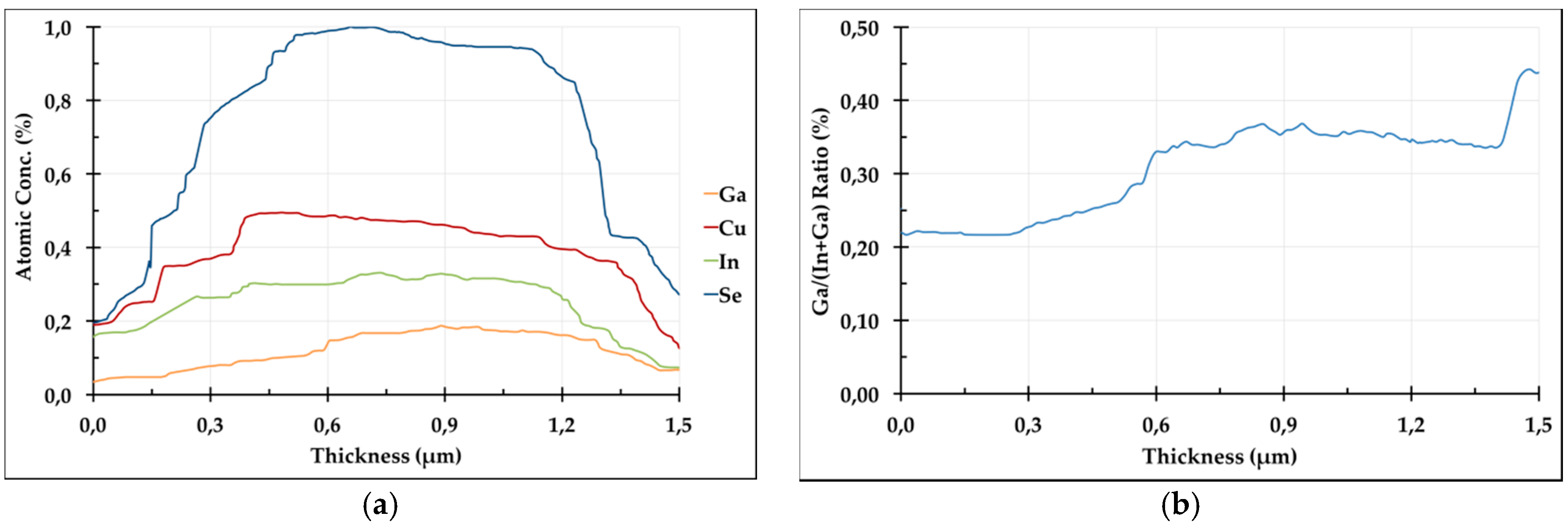
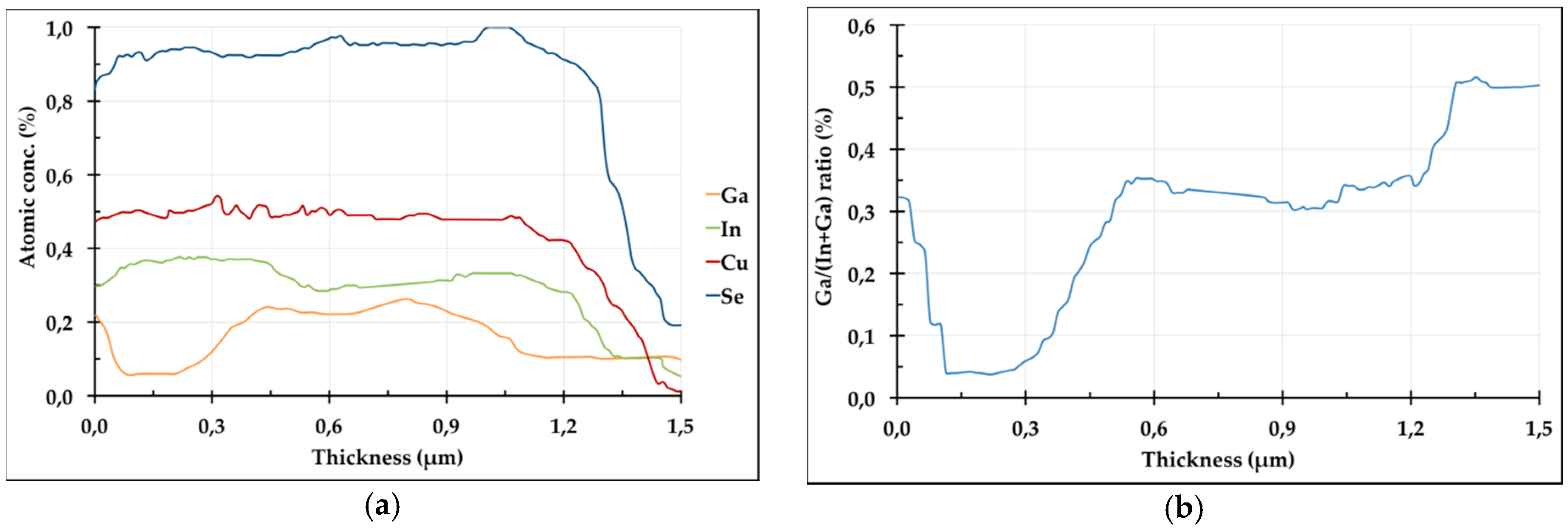
Unfortunately, the precursors prepared with the aforementioned procedure that were thought to result in a CIGS absorber layer with enhanced photovoltaic properties did not produce the desired result, as can be seen in the in-depth profile analysis obtained with secondary ion mass spectroscopy (SIMS) (
Figure 5).
Ga2Se3 is not the ideal Ga-based starting material to allow the Ga to react correctly with the other elements because it does not release enough Ga during the reaction of Cu and In with selenium. As a result, an In-rich absorber layer is obtained instead of a Ga-rich surface layer.
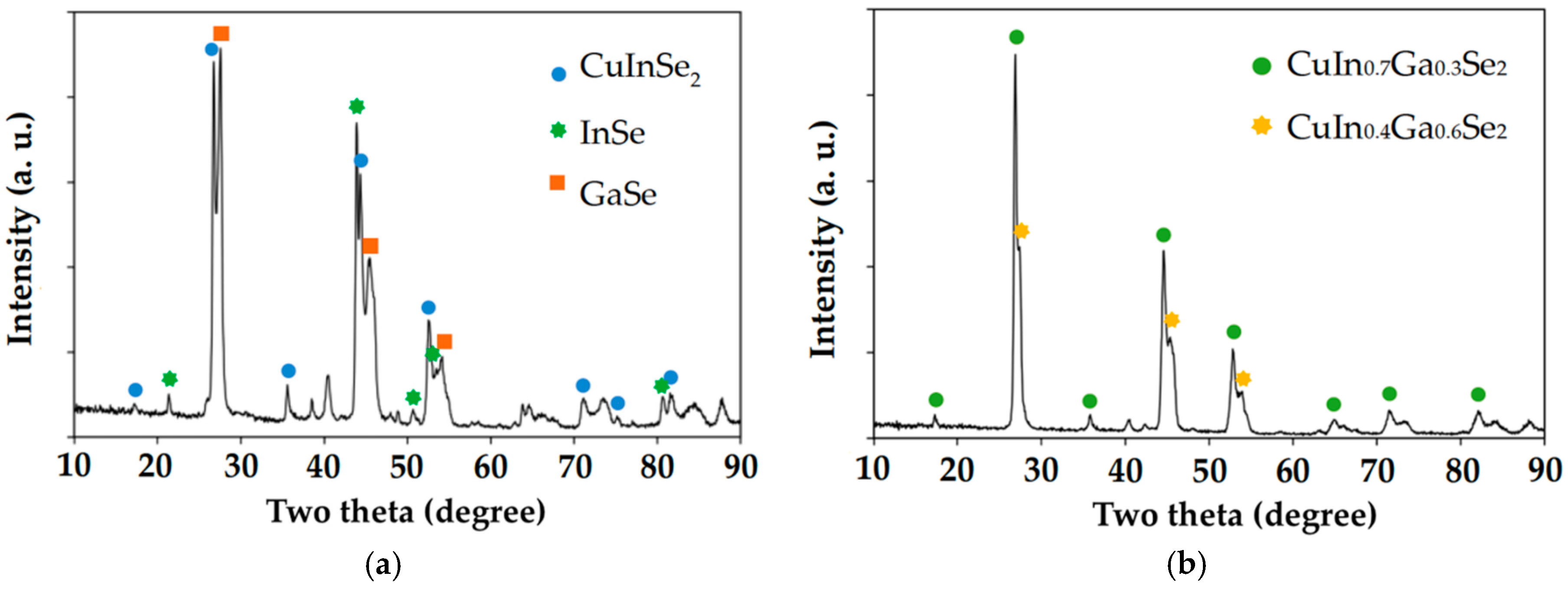
With the aim to produce solar cells of higher performance, the reactivity of the starting materials has to be adjusted to obtain an improved Ga distribution within the absorber layer. To achieve this condition, In2Se3 and Ga2Se3 precursors have to be replaced with other materials, which can interact more effectively with one another. For this purpose, In2Se3 was replaced with InSe, whereas Ga2Se3 was replaced with GaSe.
2.2. The InSe, GaSe, and Cu System
By using the process conditions already optimized for the method described above, In
2Se
3 was replaced with InSe to obtain a more effective interaction with the other constituents [
7,
13]. As InSe is more reactive than In
2Se
3, it can probably release In into the absorber material in a more uniform way. InSe allows for the formation of a better CIS matrix with the correct stoichiometry on a larger portion of the absorber, enhancing both its optical and electronic properties. The InSe film is deposited at a 670 K substrate temperature, by RF. magnetron sputtering with a 3.3 W/cm
2 power density discharge, under a 0.5 Pa argon pressure (1.2 nm/s deposition rate).
As mentioned, Ga
2Se
3 was replaced with GaSe. This material exhibits a lower melting point and decomposes at a lower temperature with respect to Ga
2Se
3. It could release Ga atoms more easily, allowing for a better interaction with the other elements, especially with copper. Furthermore, GaSe was found to have a thermal stability similar to that of Ga
2Se
3, and uniform and homogeneous polycrystalline GaSe films can be successfully obtained at deposition temperatures that are as low as 670 K. GaSe is deposited by RF magnetron sputtering, with a 1.8 W/cm
2 power density under a 0.5 Pa argon pressure (0.3 nm/s deposition rate). InSe, GaSe, and Cu were deposited in sequence as described above (
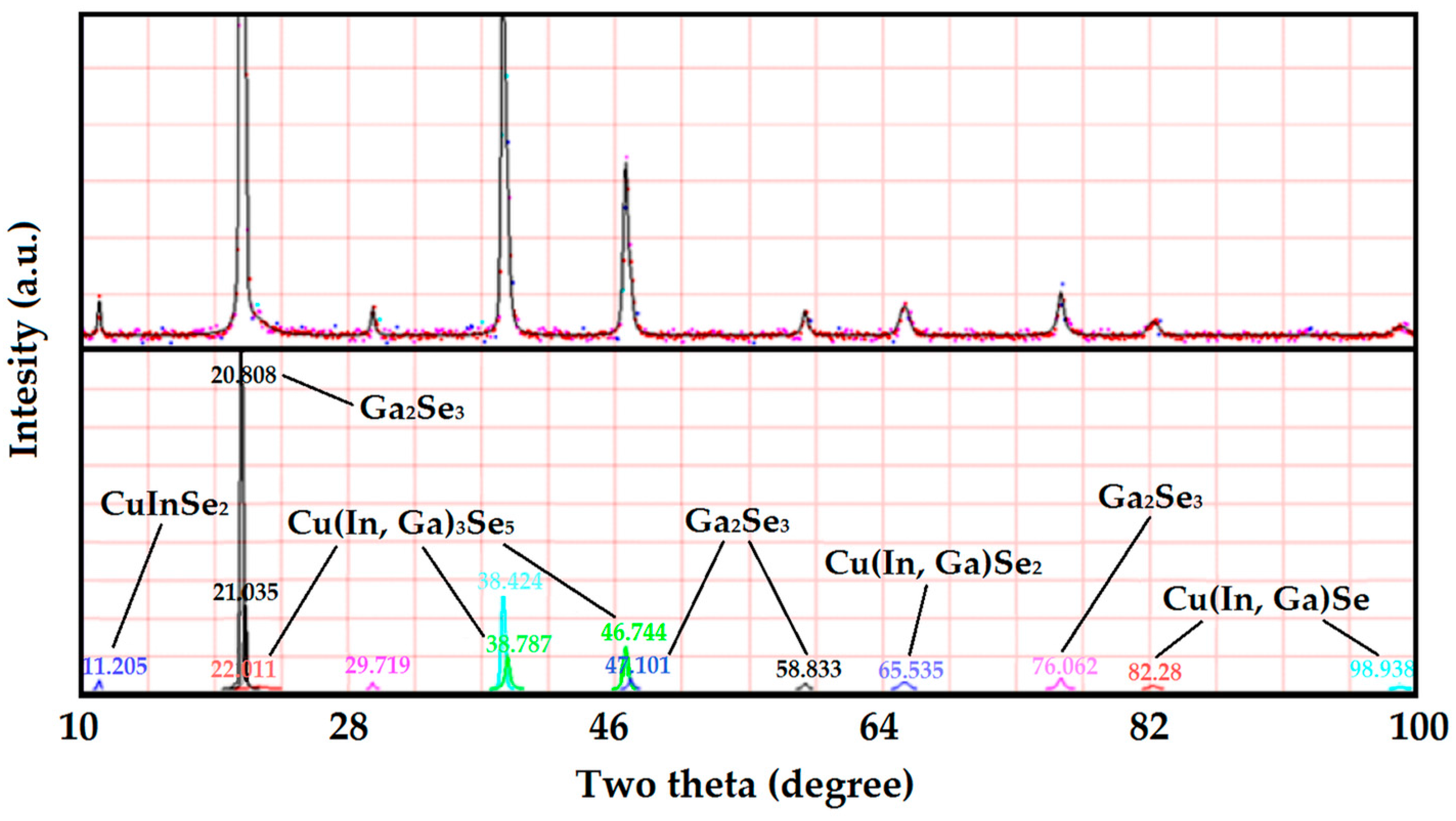
Figure 1b). In this case, Cu can be sputtered onto GaSe at the same deposition temperature (about 670 K) without causing any collateral issues inside the precursor, while improving surface uniformity. The XRD spectra of the as-deposited precursor layers and of the same film after the selenization process are showed in
Figure 6a,b respectively [
14].
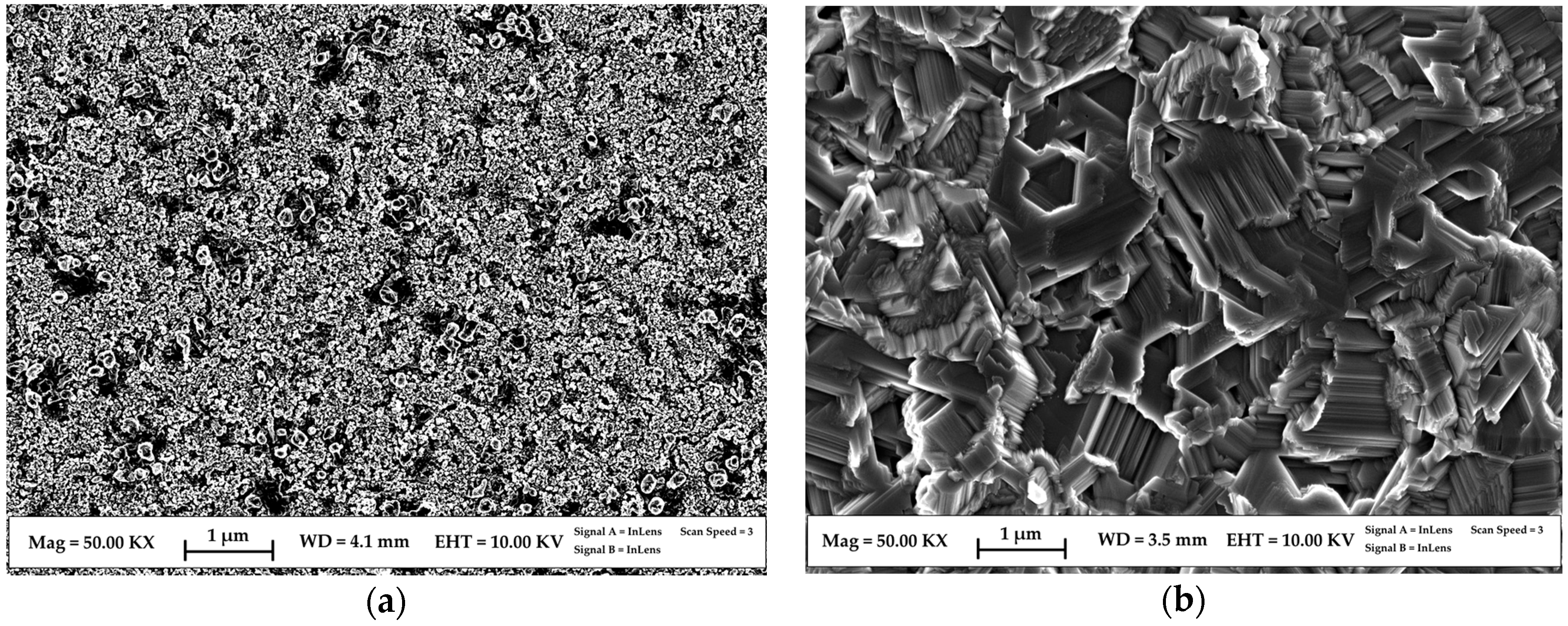
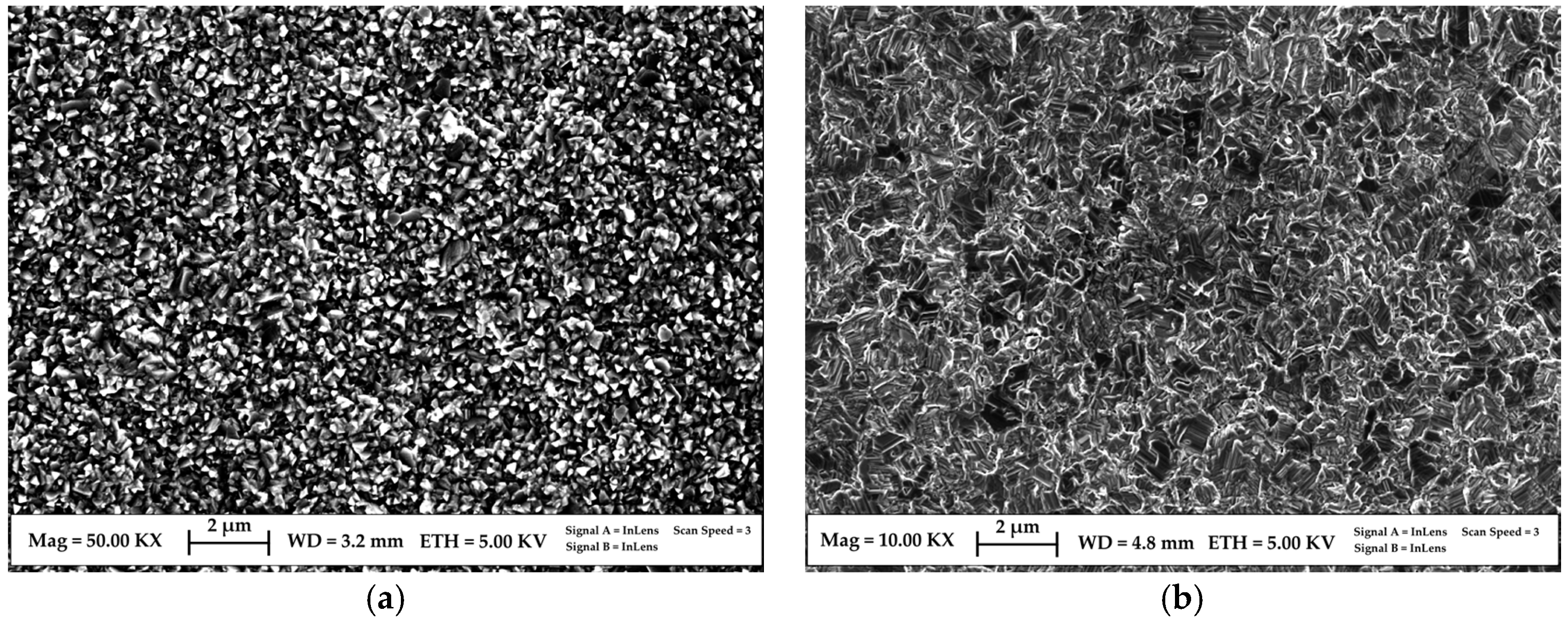
SEM images (
Figure 7) show the superficial uniformity of the precursor stack and of the absorber layer immediately after the selenization step. This CIGS film is more compact and dense when compared with the CIGS film that was prepared starting with Ga
2Se
3 and In
2Se
3, and exhibits an average grain size larger than 1 μm.
The highest photovoltaic parameters exhibited by solar cells produced with this absorber material are: V
OC = 560 mV, J
SC = 34.92 mA/cm
2, FF = 64%, and η = 12.51%. Measurements were performed at standard conditions (J-Vcurve in
Figure A1, sample #3097).
The unexpectedly low values found for VOC and FF were attributed to the fact that gallium, which is less reactive than indium, tends to diffuse towards the bottom and ends up being drained away from the film surface.
2.2.1. The InSe, GaSe, Cu, and GaSe Layers Sequence
In order to have more gallium near the surface, a change was proposed in the sequence of the layer deposition. The new sequence consists in depositing films of InSe (900 nm), GaSe (150 nm), Cu (230 nm), and GaSe (250 nm) again (
Figure 1c) on top of the initial Mo layer.
In order to eliminate the influence of individual sputter targets, whose behavior varies based on different choices of procurement, on the physical properties of the sputtered layers (stoichiometry, adhesion, thermal stability, optical and electrical behavior, etc.) the deposition parameters were changed after every target substitution. In other words, the sputtering parameters were not fixed but they were continually adjusted to obtain the desired film deposition, and this operation was carried out for all sputter targets. This was the only way to make sure the precursors films were deposited reproducibly.
The precursors are then selenized in the standard way. An analysis of the in-depth profile, performed with SIMS spectroscopy (
Figure 8), shows that this new absorber layer includes more gallium in proximity of the surface. Moving away from the surface, the Ga concentration decreases and then increases again when approaching the back contact.
The highest performing solar cells obtained with this method displayed the following parameters: V
OC = 576 mV, J
SC = 38.13 mA/cm
2, FF = 0.74 and η = 16.25%. Measurements were carried out in standard conditions (J-V characteristic in
Figure A1, sample #4025) [
15].
When the optimized stack of precursor layers (the one with an extra GaSe layer in the third method) is used, an enhanced performance of the solar cells exhibiting energy conversion efficiencies above 15%–16% is reproducibly obtained. This is probably due to the V-shaped Ga distribution, which helps to maximize both the photovoltage and the photocurrent of the solar cell. A good control of the Ga concentration is the key to engineering the profile of the energy gap of the absorbing material, which in turn plays a fundamental role in the operation of a solar cell, as explained in this article’s introduction. The detailed analysis of Ga concentration as a function of absorber layer thickness will be the subject of future studies. In particular, the optimization of the thickness of the lower Ga-concentration layer should be addressed in order to maximize the absorbing properties of the CIGS film.
2.2.2. The Ceramic Substrate
The ceramic tiles used in this work are covered with glassy enamel which has a composition similar to that of SLG. In this way, the tile surface becomes smoother, making this substrate suitable for thin film deposition. The opaque glassy enamel have typical thicknesses ranging from 300 μm up to 1000 μm. They are deposited starting from wet powders and are processed on the ceramic surface at a temperature between 1210 K and 1250 K [
16].
The structure of the precursor is composed of a 1500-nm-thick InSe film, a 200–300-nm-thick GaSe film, a 350–400-nm-thick Cu film, and, finally, a 400–500-nm-thick GaSe film as it was for the samples deposited on SLG. All the materials are deposited at a substrate temperature of 670 K, and the precursor is selenized at high temperature (790 K) in a pure-Se atmosphere. In other words, the process developed on SLG was simply transposed to the ceramic substrate, and the resulting precursor seemed to maintain a morphology of the same quality (
Figure 9).
The highest performing solar cells obtained with this method yielded the following parameters: V
OC = 610 mV, J
SC = 36.79 mA/cm
2, FF = 0.61, and η = 13.69%. Measurements were acquired at standard conditions (J-V characteristic in
Figure A1, sample #1113).
All cell parameters refer to an area of around 1 cm2 (if not expressly stated otherwise). The photovoltaic parameters were collected over 20 samples for every method. Each sample included 4 cells; therefore, we tested about 80 cells for each method to make sure that the whole fabrication process was indeed reproducible (as the standard deviation indicates). At any rate, we here reported the PV parameters of solar cells representative of each method. Generally, we have chosen to show the photovoltaic parameters of devices made with layers on which morphological, structural, and compositional investigations were carried out.
As one can see from the data in
Table 1, the photocurrent of solar cells grown on ceramic tiles is lower than the photocurrent obtained by solar cells grown on SLG. A possible explanation is that commercially available ceramic tiles are characterized by a high number of macroscopic surface defects. Voids and prominences are larger than the combined thickness of all the deposited films, which cannot fill or cover them completely. If the ceramic surface is covered by glassy enamel, with a composition similar to the SLG, the surface is much smoother, making the ceramic a suitable substrate for a thin-film deposition. The residual defectiveness requires the use of a material poorer in Cu, as compared with CIGS grown on SLG, to avoid a deleterious segregation of binary phases, such as Cu
2Se, inside the surface non-uniformities of the ceramic substrates. A Cu-poor material is obtained by increasing the In concentration. However, this has a negative influence on the Ga-concentration profile as more indium makes it flatter, inevitably leading to a loss of the benefits that come from a V-shape distribution.


