Article

Analysis and Minimization of Output Current Ripple for Discontinuous Pulse-Width Modulation Techniques in Three-Phase Inverters

1
Department of Electrical, Electronic, and Information Engineering, University of Bologna, Viale Risorgimento 2, Bologna 40136, Italy
2
Department of Engineering Sciences, Ångström Laboratory, Uppsala University, Lägerhyddsvägen 1, Box 534, Uppsala S-751 21, Sweden
*
Author to whom correspondence should be addressed.
Energies 2016, 9(5), 380; https://doi.org/10.3390/en9050380
Submission received: 5 April 2016 / Revised: 4 May 2016 / Accepted: 6 May 2016 / Published: 19 May 2016
(This article belongs to the Special Issue Power Electronics Optimal Design and Control)

Abstract

:
This paper gives the complete analysis of the output current ripple in three-phase voltage source inverters considering the different discontinuous pulse-width modulation (DPWM) strategies. In particular, peak-to-peak current ripple amplitude is analytically evaluated over the fundamental period and compared among the most used DPWMs, including positive and negative clamped (DPWM+ and DPWM−), and the four possible combinations between them, usually named as DPWM0, DPWM1, DPWM2, and DPWM3. The maximum and the average values of peak-to-peak current ripple are estimated, and a simple method to correlate the ripple envelope with the ripple rms is proposed and verified. Furthermore, all the results obtained by DPWMs are compared to the centered pulse-width modulation (CPWM, equivalent to the space vector modulation) to identify the optimal pulse-width modulation (PWM) strategy as a function of the modulation index, taking into account the different average switching frequency. In this way, the PWM technique providing for the minimum output current ripple is identified over the whole modulation range. The analytical developments and the main results are experimentally verified by current ripple measurements with a three-phase PWM inverter prototype supplying an induction motor load.

Graphical Abstract

1. Introduction

Three-phase voltage source inverters (VSIs) are widely adopted in ac motor drives, controlled rectifiers and, in general, grid-connected applications, as a means of dc-ac power conversion devices. There are two main modulation techniques exploited in past years: space vector pulse-width modulation (SV-PWM) and carrier-based pulse-width modulation (CB-PWM). In the space vector concept, the switching instants are determined by calculating the duty cycles on the basis of the available output voltage space vectors. In carrier-based modulation, the output reference voltage signals are compared to a triangular carrier waveform, and the intersections define the switching instants [1]. Early carrier-based implementations employed analogue circuits, but later on low cost digital microcontrollers have enforced the viability of digital timers/comparators to realize pulse-width modulation (PWM) units. Nowadays, most of VSI applications employ carrier-based modulation schemes due to their simplicity of implementation, in both analogue and digital ways [2,3].
In three-phase systems, the PWM approach leads to a degree of freedom in the modulation process. In the space vector modulation (SVM), this degree of freedom appears in partitioning the two zero states. In the carrier-based modulation the degree of freedom appears as a common-mode signal that can be injected to the reference voltage waveforms. In both modulation techniques, output waveforms quality and switching losses are affected by the choice of this degree of freedom. It is proven that a proper common-mode signal injection in CB-PWM leads to the same switching pattern as in SV-PWM [4]. By equally sharing the application time of two zero states, the so-called “centered” switching pattern is obtained. The centered modulation is known to be the best one in terms of current ripple rms minimization [3,5,6].
The so-called “discontinuous” pulse-width modulation (DPWM) allows reducing the average switching frequency, which is particularly suitable for high-power inverters [7]. Theoretically, considering the same switching period (i.e., the same carrier frequency), DPWM gives a 1/3 reduction of the average switching frequency compared to continuous PWMs, saving 33% of the switching losses. In fact, in discontinuous PWM, the switches of one inverter leg cease commutations for 1/3 of the fundamental period. The consequence is that associated output phase is clamped to the positive (DPWM+) or negative (DPWM−) dc rail and the switching losses of the associated inverter leg are eliminated.
Two modulators with discontinuous modulation waves, classified as discontinuous PWM Depenbrock’s method [8] (hereinafter referred to as DPWM1) and Ogasawara’s method [9] (hereinafter referred to as DPWM2), have gained recognition first. The low harmonic distortion at high modulation indexes and the controllability of the switching losses were proven for these two methods.
The other popular balanced discontinuous PWM methods (DPWM0 and DPWM3) are the combination of the DPWM+ and DPWM− [2,3,4,5,10,11], with difference in the modulator phase angle, as depicted in Figure 1 and Figure 2. Besides the basic discontinuous modulations (DPWM−, DPWM+, DPWM0, DPWM1, DPWM2, and DPWM3), different generalized discontinuous PWMs (GDPWMs) have been proposed, having optimized the switching losses over the entire modulation range and reaching superior high modulation ranges [10,11]. More recently, different discontinuous modulations have been proposed for multilevel inverters as well [12,13].
For all the discontinuous modulation techniques, current ripple rms and switching losses, being the two important modulator characteristics, have been addressed in deep and compared with other popular modulation techniques: [1,2,3,4,5,14]. In particular, among the basic discontinuous modulation techniques, the DPWM3 was found to be the optimal one, whereas the DPWM1 was found to be the worst. It has been proven that DPWMs show even better behavior compared to SVPWM for high modulation indexes and considering the same average switching frequency [5,10].
Recently, the importance of the calculation of current ripple peak-to-peak envelope has been recognized in addition to the rms analysis [15,16], and it has been analyzed for three-phase [17,18,19,20,21,22] and multiphase inverters [23]. The current ripple peak-to-peak amplitude has been analyzed partially also for the discontinuous modulation [20], comparing the two modulation techniques, i.e., SVPWM and DPWM1. However, the calculation of the current ripple peak-to-peak and further analysis includes only the DPWM1 method, lacking in depth and details.
In general, in terms of the importance and applications, the peak-to-peak current ripple distribution is crucial for the estimation of the multiple zero-crossing intervals of the output current and the corresponding dead-time output voltage distortion in order to compensate for the inverter nonlinearities [24,25]. Moreover, knowledge of current ripple amplitude can be used to compare different PWM with hysteresis current controllers [26], and to define variable switching frequency PWM techniques [27]. Another possible application can be seen in the design and control of the active and passive grid filters [28].
The complete analysis and comparison of the output current ripple distribution in three-phase VSIs for the different DPWMs is given in this paper. In particular, peak-to-peak current ripple amplitude is evaluated and compared among the most used discontinuous modulations, including the two basic positive and negative clamped, and their four derived balanced solutions. The analysis has been developed taking into account the same switching period as well as same average switching frequency. In addition to the peak-to-peak amplitude distribution over the fundamental period, the average and the maximum values of current ripple are derived, and a simple method to correlate the ripple envelope with the ripple rms is proposed and verified. The instantaneous current ripple is determined for a generic balanced three-phase load consisting of series RL impedance and ac back electromotive force (RLE-load), representing both motor-load and grid-connected applications. For the sake of simplicity, the first phase of three-phase system is considered for the analysis. Furthermore, all the results obtained by discontinuous PWMs are compared to the continuous PWM to identify the most optimal PWM strategy. The analytical developments and the main results are experimentally verified by a three-phase inverter prototype supplying an induction motor load.

2. Problem Statement and Basic Equations

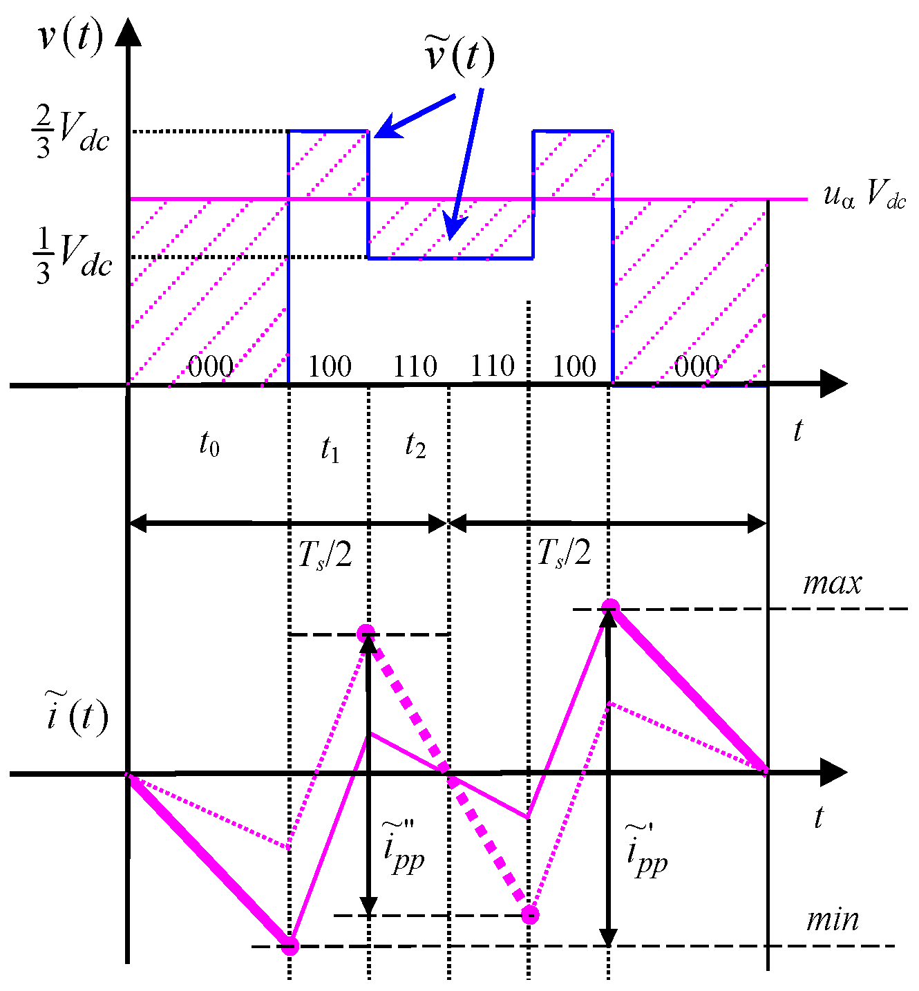
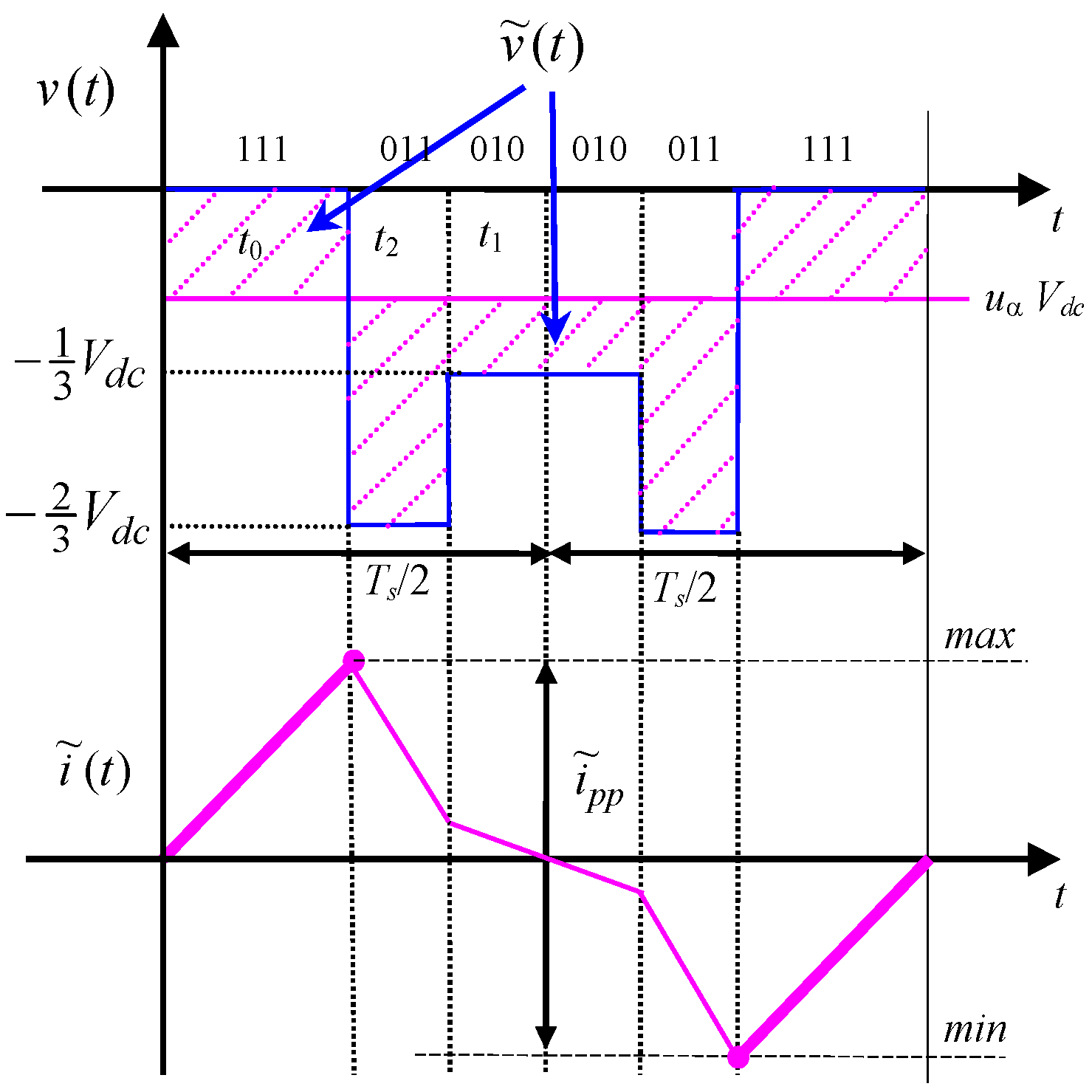
2.1. Load Model and Current Ripple Definitions

Considering a three-phase voltage source inverter either supplying an ac motor or connected to the grid by link inductors, the instantaneous current ripple i ˜ ( t ) can be determined for each phase according to [18,21], on the basis of the alternating voltage component v ˜ ( t ) :
i ˜ ( t ) = 1 L 0 t v ˜ ( t ) d t
being:
v ˜ ( t ) = v ( t ) v ¯ ( T s )
where v(t) is the instantaneous output voltage, v ¯ ( T s ) is the average output voltage over the inverter switching period Ts, and L is either the total leakage inductance of ac motor or the link inductance towards the grid. Resistive voltage drops can usually be neglected [18,21].
In terms of space vectors, focusing on the first phase of the balanced three-phase system, variables are given by projecting the corresponding space vectors on the real axis. In particular, within the linear modulation range, i.e., m = [0, 1/ 3 ], the average output voltage over the switching period corresponds to the reference voltage v*, and it is given by:
v ¯ ( T s ) = v * = Re { v * } = V *   cos ϑ = m V dc cos ϑ
Equations (1)–(3) allow determining the instantaneous current ripple as:
i ˜ ( t ) = 1 L 0 t [ v ( t ) m V dc cos ϑ ] d t
Finally, the peak-to-peak amplitude of current ripple within the switching period can be calculated as:
i ˜ pp = max { i ˜ ( T s ) } min { i ˜ ( T s ) }

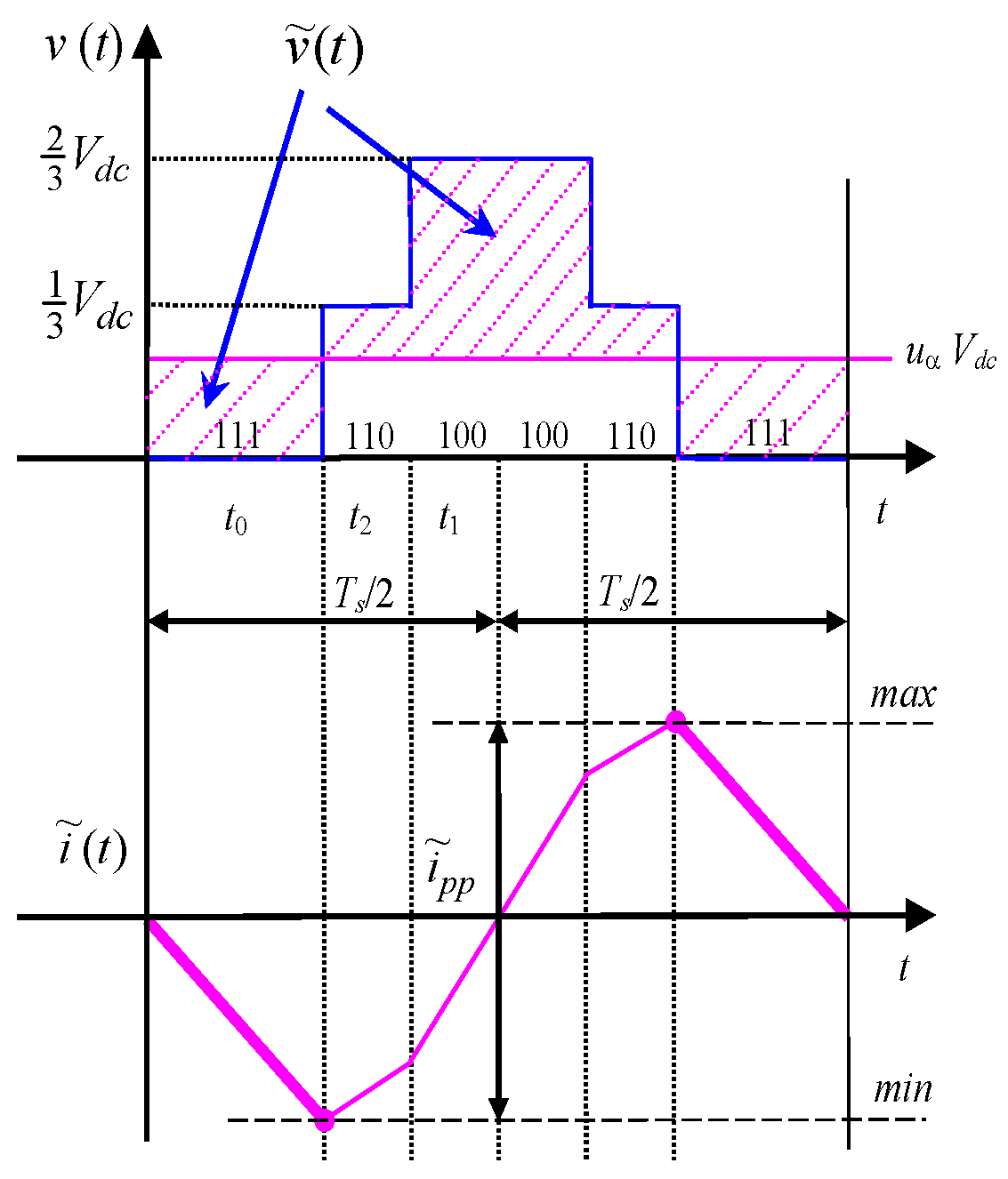
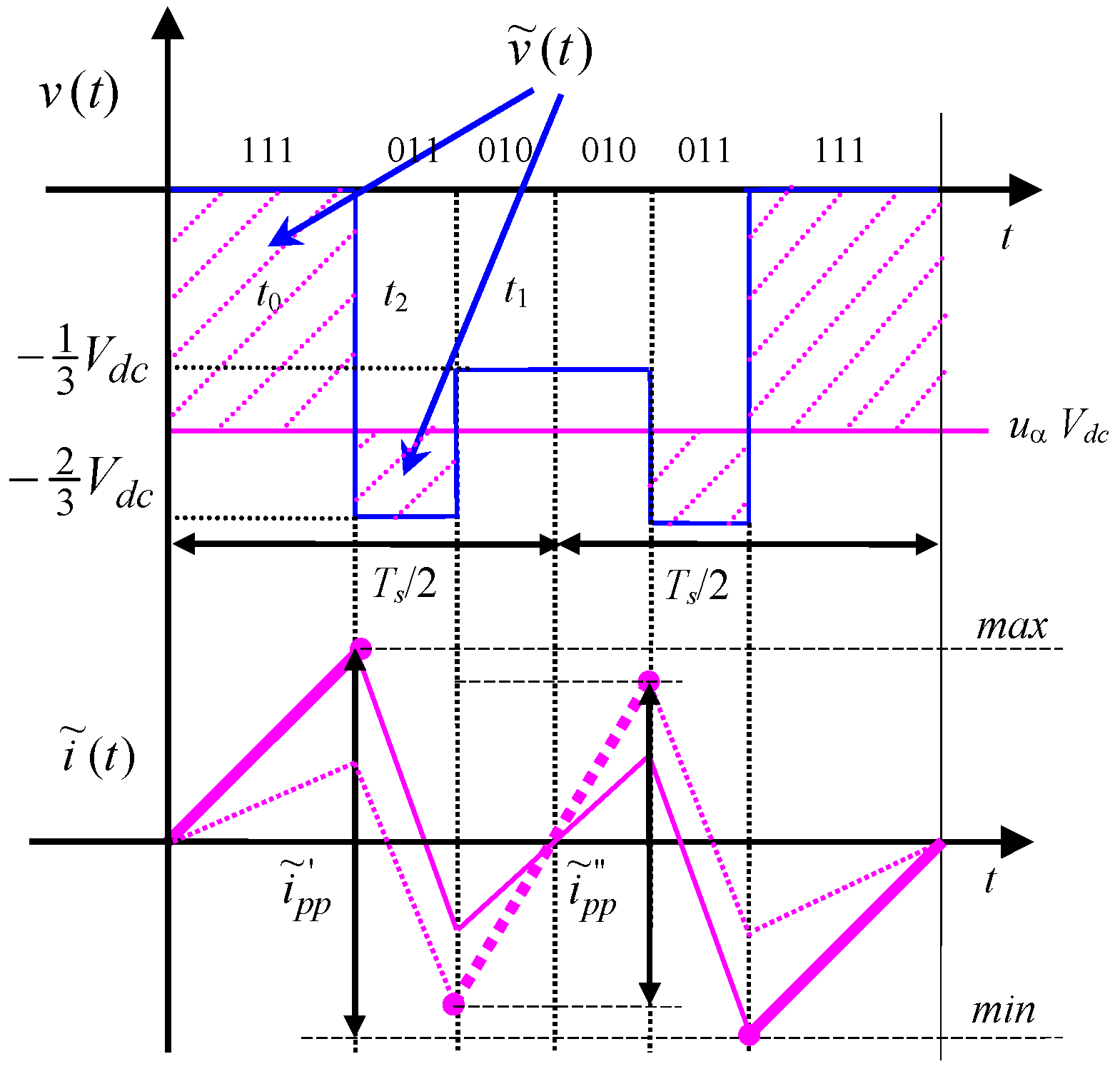
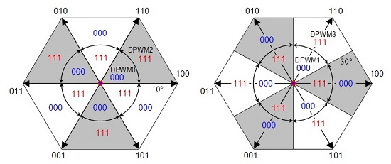
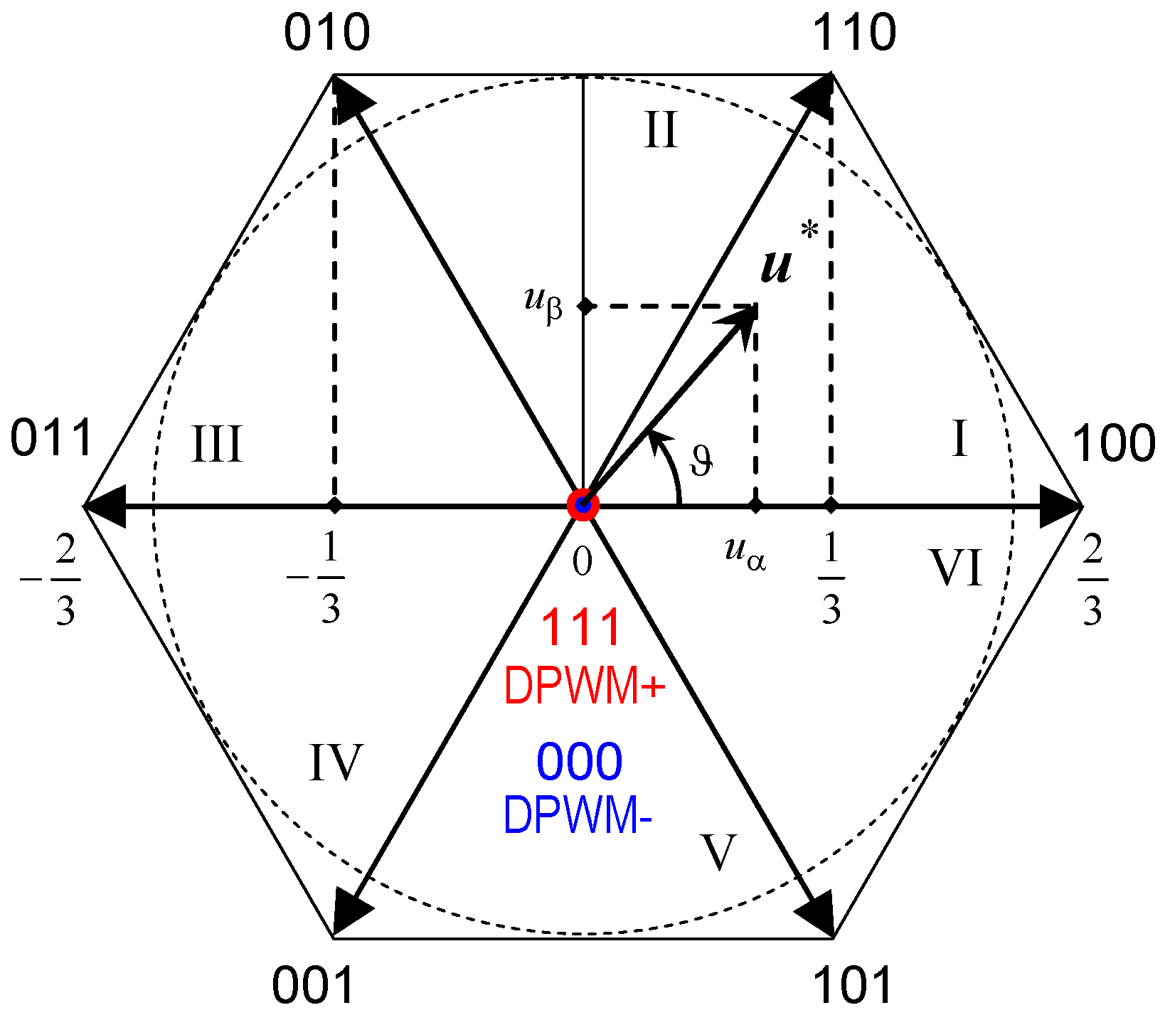
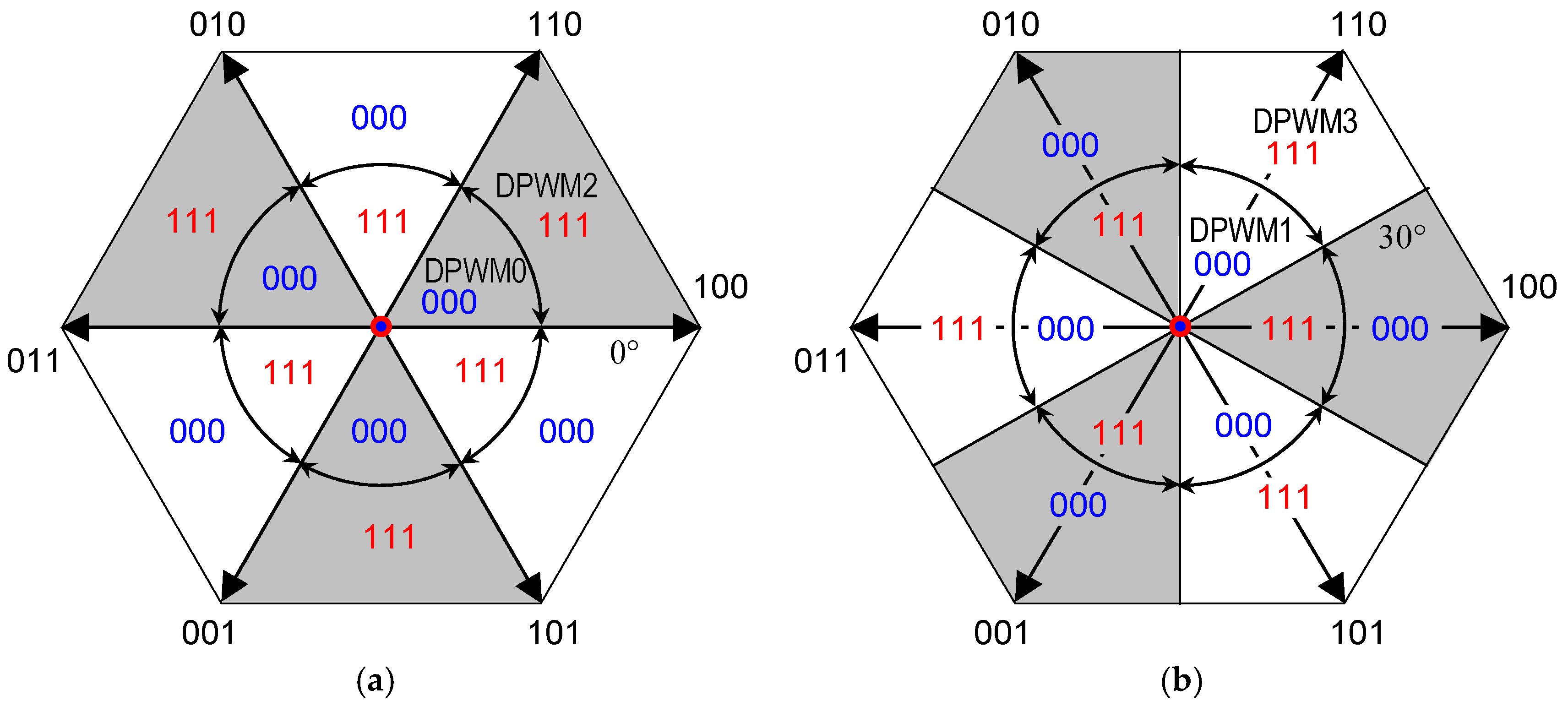
2.2. Space Vector Discontinuous Pulse-Width Modulation

The SVM of three-phase inverters is based on the determination of application times of active and null inverter voltage vectors in every switching period Ts. In general, carried-based PWM offers the well-known advantages over SV-PWM such as an inherent simplicity, flexibility, reduced computational time, and easy implementation on industrial DSPs, without the need of FPGA or any other additional hardware. On the other hand, the SVM approach offers a simpler key in understanding the modulation process with a straight and effective method to calculate the application times (duty-cycles). Denoting the switching states of the k-th inverter phase as Sk = [0,1], the output voltage vector v can be expressed as:
v = 2 3 [ S 1 + S 2 α + S 3 α 2 ] V dc
where Vdc is the dc supply voltage and α = exp(j2π/3).
Figure 1 shows the output voltage space vectors corresponding to all possible switch configurations. It appears to be a hexagon with six sectors numbered I–VI. There are two redundant states corresponding to the null vector (000 and 111). SV-PWM scheme uses the nearest three vectors (NTV) algorithm to approximate the reference output voltage vector. In the case of continuous PWM, the switching sequence starts from one zero state, goes to the other zero state through the two active states, and symmetrically comes back to the beginning, with a single leg commutation for each step. By equally sharing the application time of the null voltage vector between the switch configurations 000 and 111, the so-called “centered” switching pattern is realized and nearly-optimal modulation, able to minimize the rms of current ripple, is obtained [5].
Considering the discontinuous PWM, there are two basic implementations: the so-called positive bus clamped (DPWM+) and the negative bus clamped (DPWM−). Namely, DPWM+ does not use the state 000, while DPWM− does not use the state 111, as shown in Figure 1. In terms of carrier-based modulation, the implementation is possible by a different common-mode signals injection [2,3].
In order to balance the usage of the six inverter switches within the fundamental period, a suitable combination of positive and negative clamped DPWMs can be considered. In particular, DPWM0, DPWM1, DPWM2, and DPWM3 are obtained by alternating the DPWM+ and DPWM− every 60°, as represented by the grey colored sectors in Figure 2. In Figure 2a, DPWM0 and DPWM2 are depicted, starting at 0° with DPWM− and DPWM+, respectively, whereas in Figure 2b DPWM1 and DPWM3 are depicted, starting at 30° with DPWM−and DPWM+ respectively.
Application times tk of NTV are defined by duty-cycles δ1, δ2, and δ0 and switching period Ts, being δk = tk/(Ts/2). Duty-cycles for half of the fundamental period, i.e., for the three first sectors of Figure 1 (0 ≤ ϑ ≤ 60°, 60° ≤ ϑ ≤ 120°, and 120° ≤ ϑ ≤ 180°), are given in Table 1 on the basis of normalized reference voltage components uα and uβ, depicted in Figure 1 and defined as:
{ u α = m cos ϑ u b = m sin ϑ

3. Evaluation of Output Current Ripple

In order to evaluate the output current ripple, the output voltage levels in each switching period should be identified with the corresponding application times. Starting from the output voltage vector given in Equation (6), the instantaneous output voltage of the 1st phase can be expressed by switching states, leading to:
v ( t ) = [ S 1 1 3 ( S 1 + S 2 + S 3 ) ] V dc = u ( t ) V dc
The alternating voltage component can be determined by introducing Equations (3), (7), and (8) in Equation (2):
v ˜ ( t ) = [ S 1 1 3 ( S 1 + S 2 + S 3 ) ] V dc m cos ϑ V dc = [ S 1 1 3 ( S 1 + S 2 + S 3 ) u α ] V dc
In order to evaluate the output current ripple for all the four possible balanced discontinuous modulations (DPWM0-3), the current ripple for the two basic discontinuous modulations (DPWM±) is evaluated first, just considering half fundamental period, i.e., the three sectors of the voltage space vector hexagon: 0 ≤ ϑ ≤ 60°, 60° ≤ ϑ ≤ 120°, and 120° ≤ ϑ ≤ 180°, due to the half-wave symmetry. The results are readily extended to the four cases DPWM0-3 by swapping the two cases DPWM± every 60°, according to Figure 2. Reference is made to Figure 1 for sectors and voltage components.

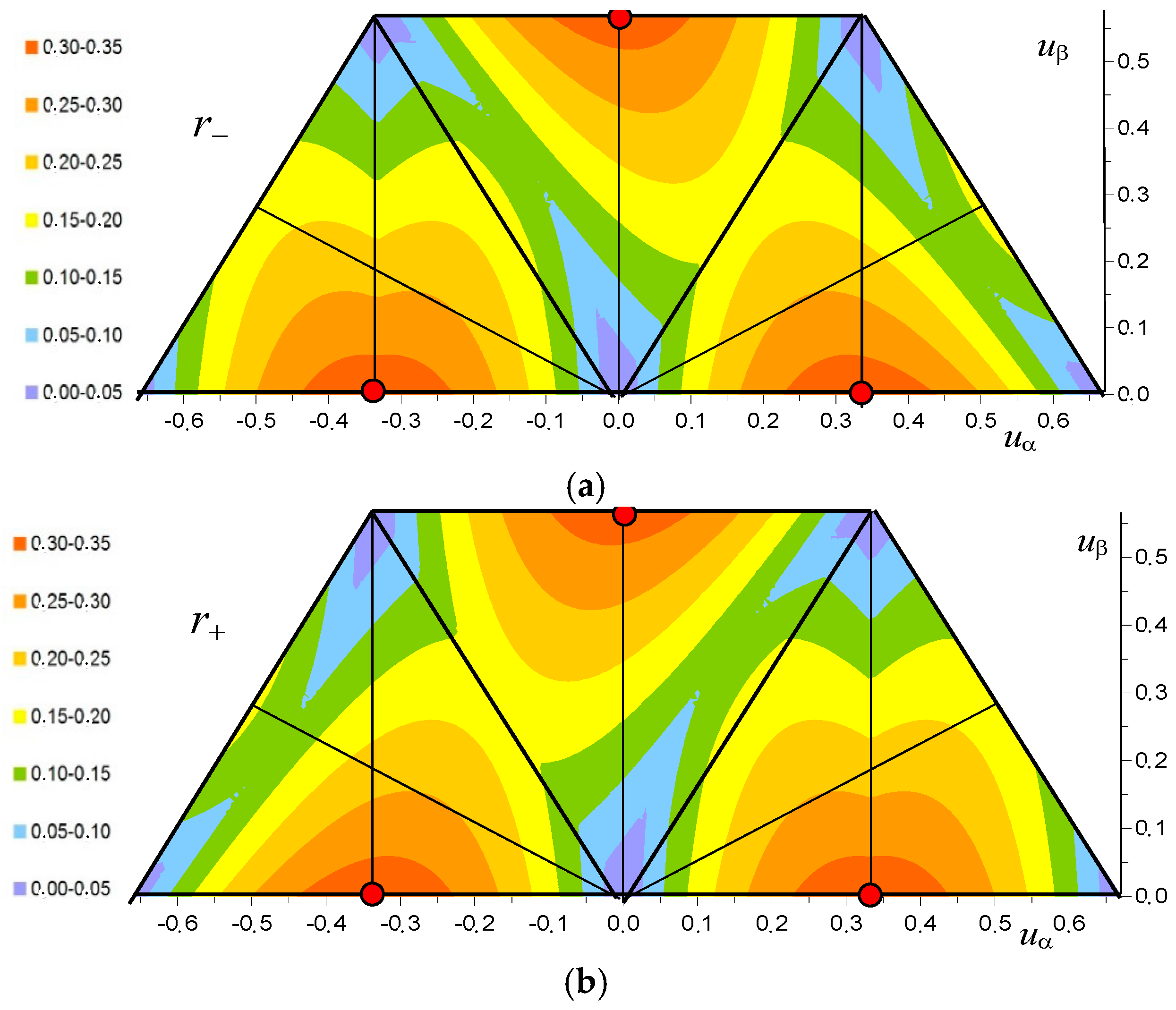
3.1. Negative Clamped Discontinuous Pulse-Width Modulation (DPWM−)

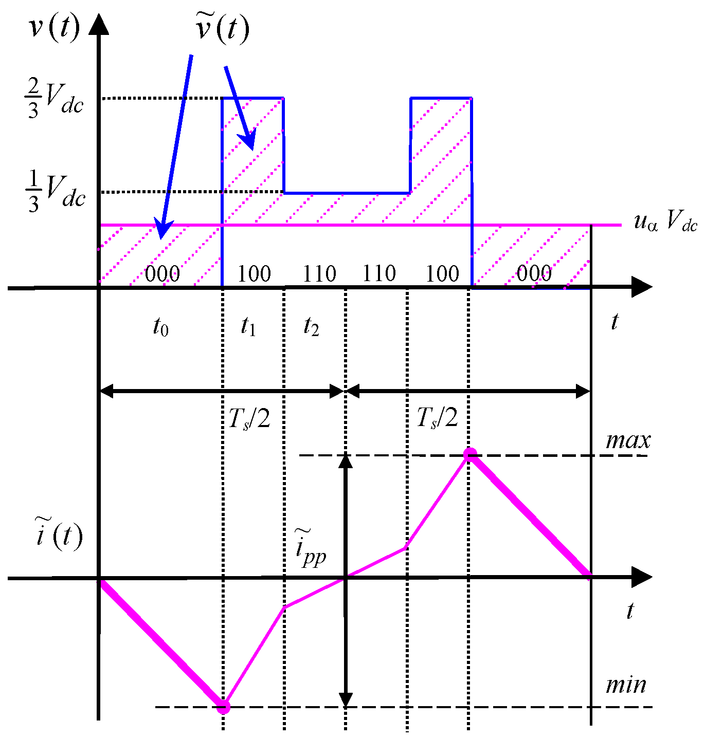
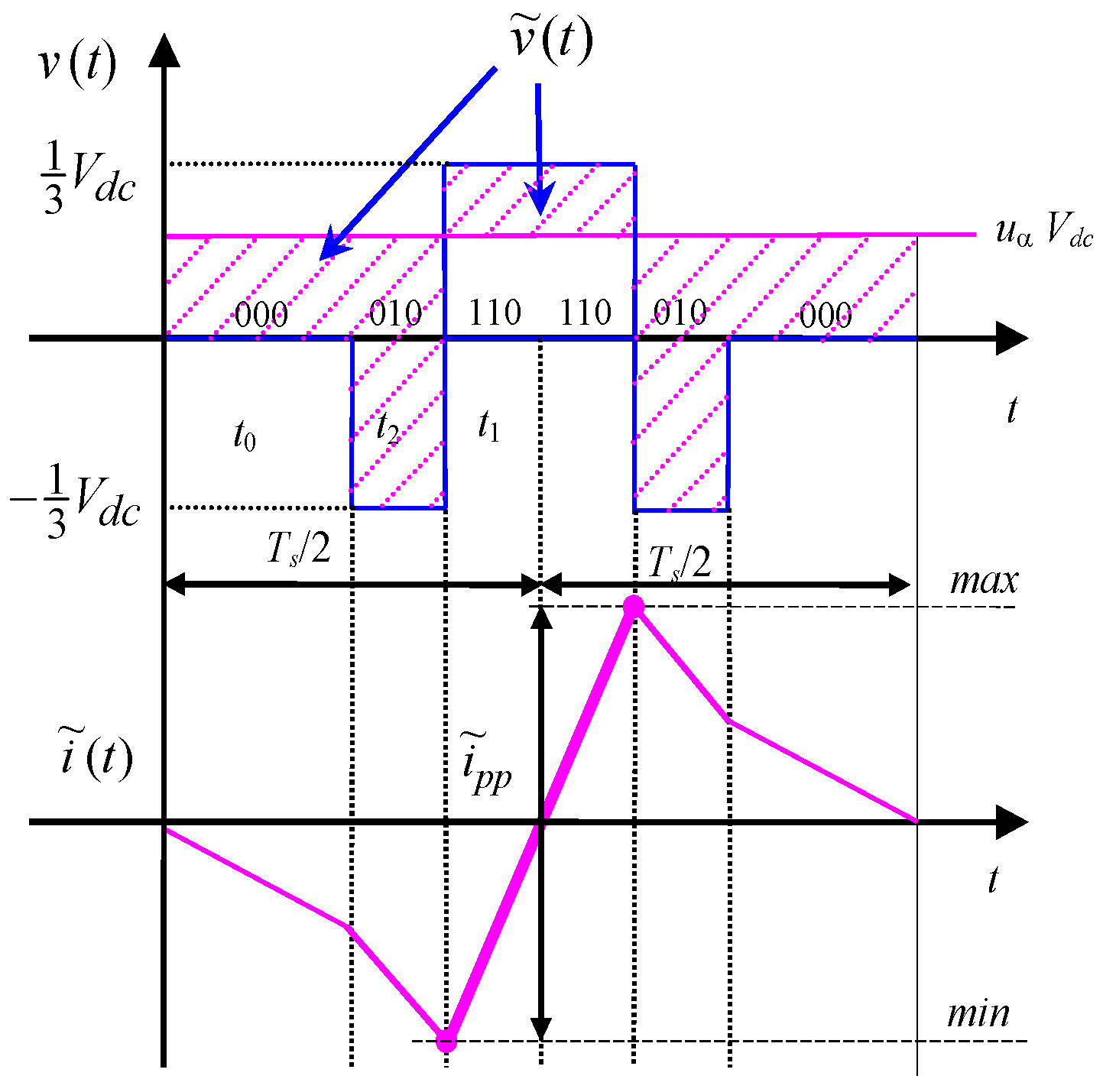
3.1.1. Evaluation of Current Ripple in Sector I

Considering sector I, 0 ≤ ϑ ≤ 60°, two different cases are considered to identify the peak-to-peak current ripple amplitude: 0 ≤ uα ≤ 1/3 and uα ≥ 1/3 (within the linear modulation limits given by the hexagon in Figure 1).
In the case of 0 ≤ uα ≤ 1/3, the current ripple i ˜ and its peak-to-peak value i ˜ pp are depicted in Figure 3, together with the instantaneous output voltage v(t). According to Figure 3, i ˜ pp can be evaluated by Equations (1), (5), and (9), considering application interval t0 or duty-cycle δ0, leading to:
i ˜ pp = 2 L { V dc m cos ϑ   t 0 } = V dc T s 2 L 2 { u α   δ 0 }
Peak-to-peak current ripple can also be expressed by introducing the normalized current ripple r as:
{ r = 2 L V dc T s i ˜ pp i ˜ pp = V dc T s 2 L r
Considering the expression of δ0 given in Table 1 for sector I and comparing Equations (10) with (11), normalized current ripple becomes:
r = 2 { u α [ 1 3 2 ( u α + 1 3 u β ) ] } = 2 u α 3 u α ( u α + 1 3 u β )
Normalized ripple r = r(uα, uβ) can be expressed as the function of modulation index m and phase angle ϑ, r = r(m,ϑ), by introducing the expression of normalized voltage components Equation (7).
The case uα ≥ 1/3 is represented in Figure 4. In this case, there are two possible values eligible for i ˜ pp , one is i ˜ pp ' determined by the duty-cycle δ0 (continuous line), and the other is i ˜ pp " determined by the duty-cycle δ2 (dashed line).
The first case (duty-cycle δ0) gives:
i ˜ pp ' = V dc T s L { u α   δ 0 }
Introducing in Equation (13) the expression of δ0 given in Table 1 for sector I, the normalized current ripple becomes:
r = 2 u α 3 u α ( u α + 1 3 u β )
The second case (duty-cycle δ2) gives:
i ˜ pp " = V dc T s L { [ u α 1 3 ] δ 2 }
Introducing in Equation (15) the expression of δ2 given in Table 1 for sector I, the normalized current ripple becomes:
r ′′ = 2 3 u β [ u α 1 3 ]
Comparing the two possible cases Equations (14) and (16), the normalized current ripple can be calculated by their maximum:
r = max { 2 u α 3 u α ( u α + 1 3 u β ) 2 3 u β [ u α 1 3 ]

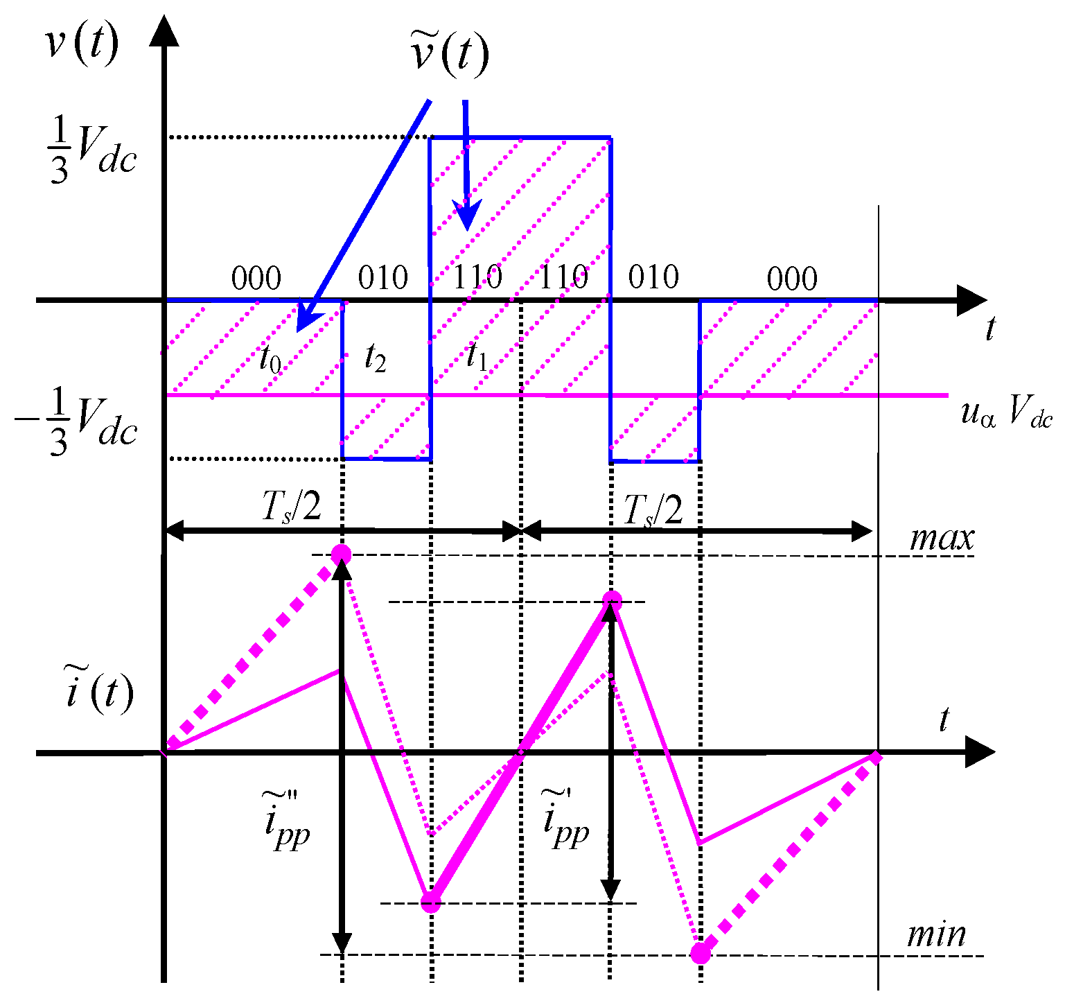
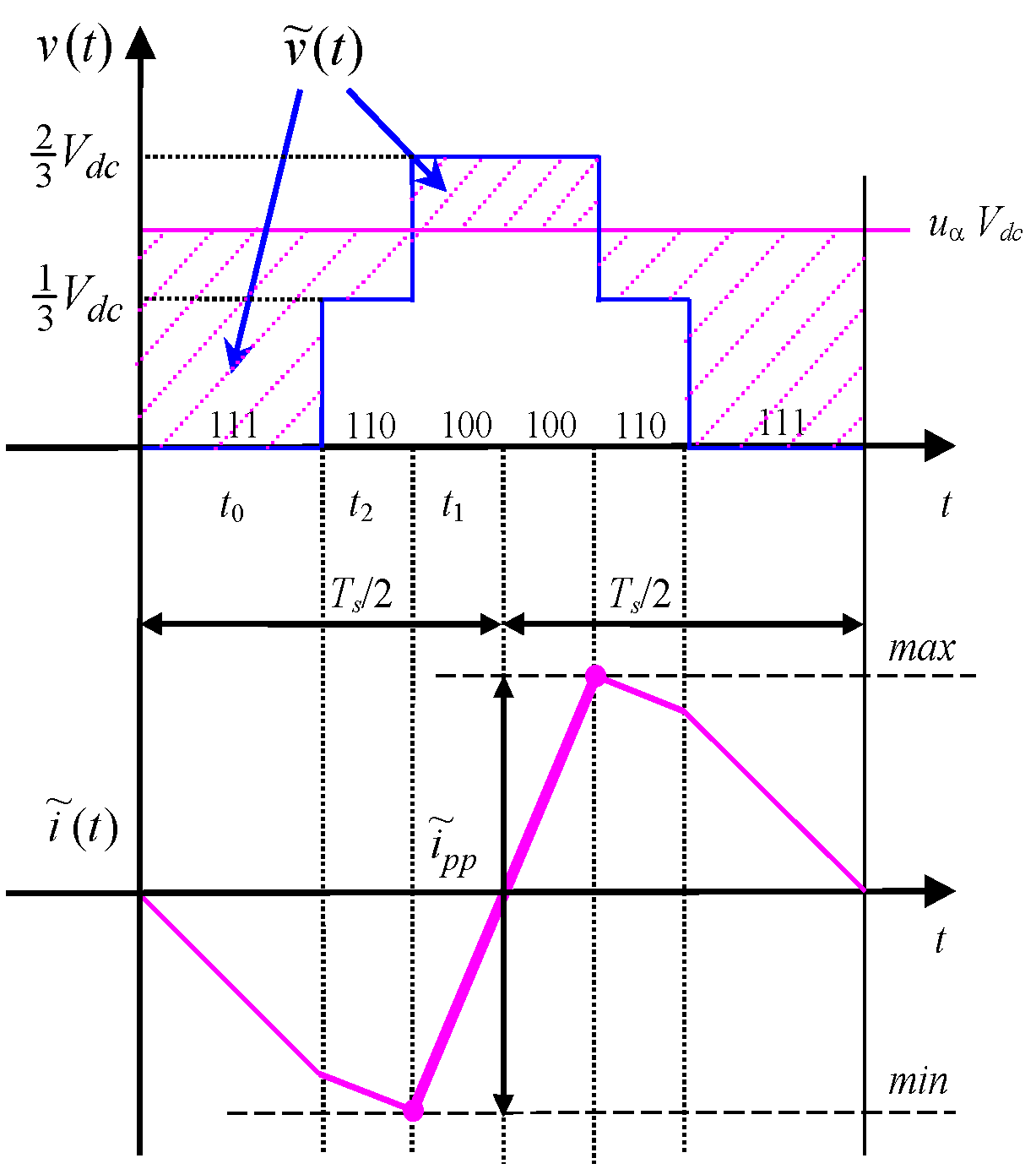
3.1.2. Evaluation of Current Ripple in Sector II

Considering sector II, 60° ≤ ϑ ≤ 120°, two different cases are considered to identify the peak-to-peak current ripple amplitude: 0 ≤ uα ≤ 1/3 and −1/3 ≤ uα ≤ 0.
In the case 0 ≤ uα ≤ 1/3, the current ripple i ˜ and its peak-to-peak value i ˜ pp are depicted in Figure 5, together with the instantaneous output voltage v(t). According to Figure 5, i ˜ pp can be evaluated by Equations (1), (5), and (9), considering the duty-cycle δ1, leading to:
i ˜ pp = V dc T s L { [ 1 3 u α ] δ 1 }
Introducing in Equation (18) the expression of δ1 given in Table 1 for sector II, the normalized current ripple becomes:
r = 3 [ 1 3 u α ] ( u α + 1 3 u β )
The case of −1/3 ≤ uα ≤ 0 is represented in Figure 6. Also in this case, there are two possible values eligible for i ˜ pp , one is i ˜ pp ' given by the duty-cycle δ1 (continuous line), and the other is i ˜ pp " given by the duty-cycle δ0 (dashed line).
The first case (duty-cycle δ1) gives:
i ˜ pp = V dc T s L { [ 1 3 u α ] δ 1 }
Introducing in Equation (20) the expression of δ1 given in Table 1 for sector II, the normalized current ripple becomes:
r = 3 [ 1 3 u α ] ( u α + 1 3 u β )
The second case (duty-cycle δ0) gives:
i ˜ pp " = V dc T s L { u α δ 0 }
Introducing in Equation (22) the expression of δ0 given in Table 1 for sector II, the normalized current ripple becomes:
r ′′ = 2 u α ( 1 3 u β )
Comparing the two possible cases Equations (21) and (23), the normalized current ripple can be calculated by their maximum:
r = max { 2 u α ( 1 3 u β ) 3 [ 1 3 u α ] ( u α + 1 3 u β )

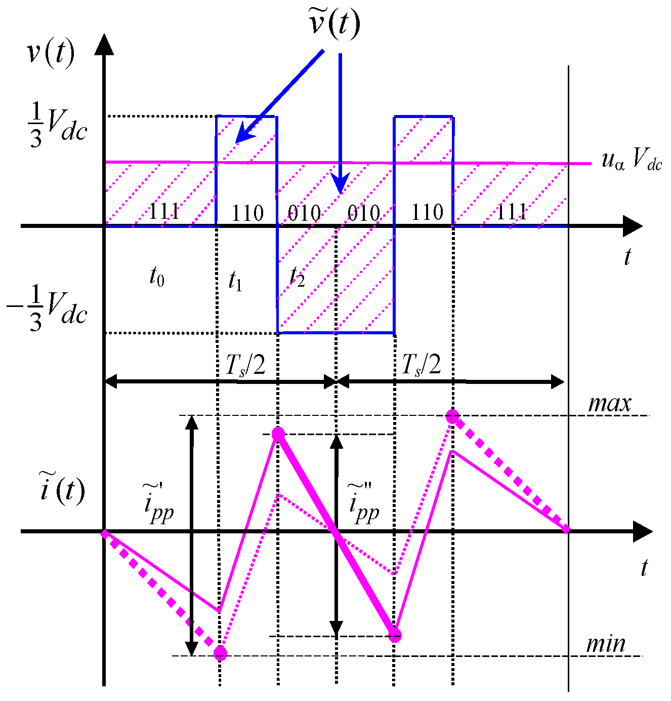
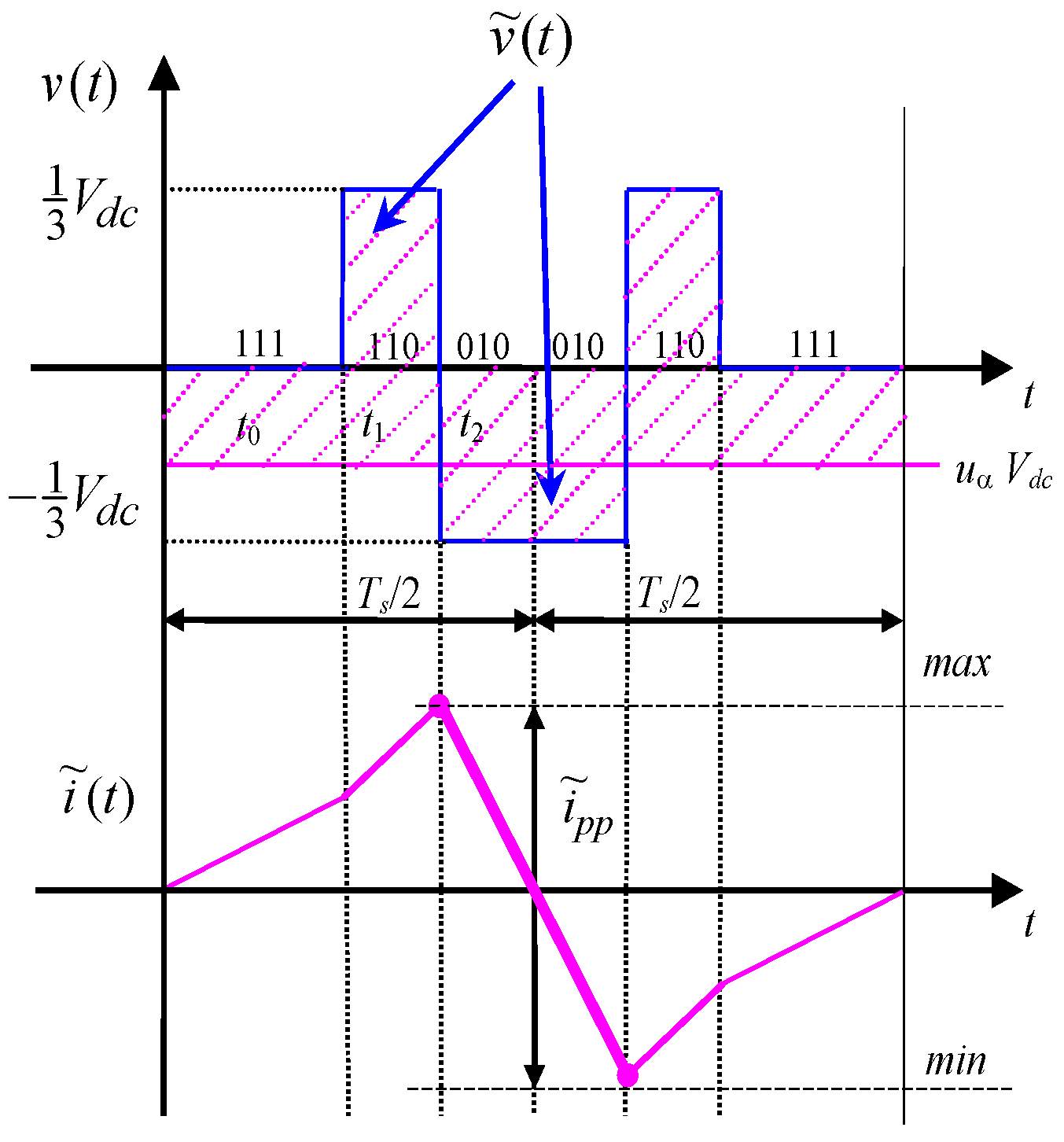
3.1.3. Evaluation of Current Ripple in Sector III

Considering sector III, 120° ≤ ϑ ≤ 180°, two different cases are considered to identify the peak-to-peak current ripple amplitude: −1/3 ≤ uα ≤ 0 and uα ≤ −1/3 (within the linear modulation limits given by the hexagon in Figure 1).
In the case −1/3 ≤ uα ≤ 0, the current ripple i ˜ and its peak-to-peak value i ˜ pp are depicted in Figure 7, together with the instantaneous output voltage v(t). According to Figure 7, i ˜ pp can be evaluated by Equations (1), (5), and (9), considering the duty-cycle δ0, leading to:
i ˜ pp = V dc T s L { u α δ 0 }
Introducing in Equation (25) the expression of δ0 given in Table 1 for sector III, the normalized current ripple becomes:
r = 2 u α + 3 u α ( 1 3 u β u α )
The case uα ≤ −1/3 is represented in Figure 8. In this case i ˜ pp can be evaluated considering the duty-cycle δ2, leading to:
i ˜ pp = V dc T s L { [ 2 3 + u α ] δ 2 }
Introducing in Equation (27) the expression of δ2 given in Table 1 for sector III, the normalized current ripple becomes:
r = 3 [ 2 3 + u α ] ( 1 3 u β u α )

3.2. Positive Clamped Discontinuous Pulse-Width Modulation (DPWM+)

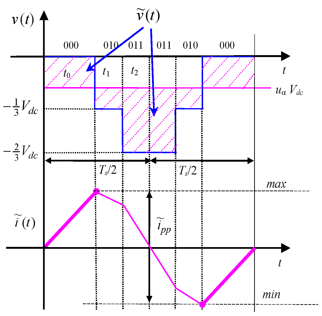
3.2.1. Evaluation of Current Ripple in Sector I

Considering sector I, 0 ≤ ϑ ≤ 60°, two different cases are considered to identify the peak-to-peak current ripple amplitude: 0 ≤ uα ≤ 1/3 and uα ≥ 1/3 (within the modulation limits given by the hexagon in Figure 1).
In the case of 0 ≤ uα ≤ 1/3, the current ripple i ˜ and its peak-to-peak value i ˜ pp are depicted in Figure 9, together with the instantaneous output voltage v(t). According to Figure 9, i ˜ pp can be evaluated by Equations (1), (5), and (9), considering application interval t0 or duty-cycle δ0, leading to:
i ˜ pp = V dc T s L { u α δ 0 }
Considering the expression of δ0 given in Table 1 for sector I and introducing it in Equation (29), normalized current ripple becomes:
r = 2 u α 3 u α ( u α + 1 3 u β )
The case uα ≥ 1/3 is depicted in Figure 10. In this case i ˜ pp can be evaluated considering the duty-cycle δ1, leading to:
i ˜ pp = V dc T s L { [ 2 3 u α ] δ 1 }
Introducing in Equation (31) the expression of δ1 given in Table 1 for sector I, the normalized current ripple becomes:
r = 3 ( 2 3 u α )   ( u α 1 3 u β )

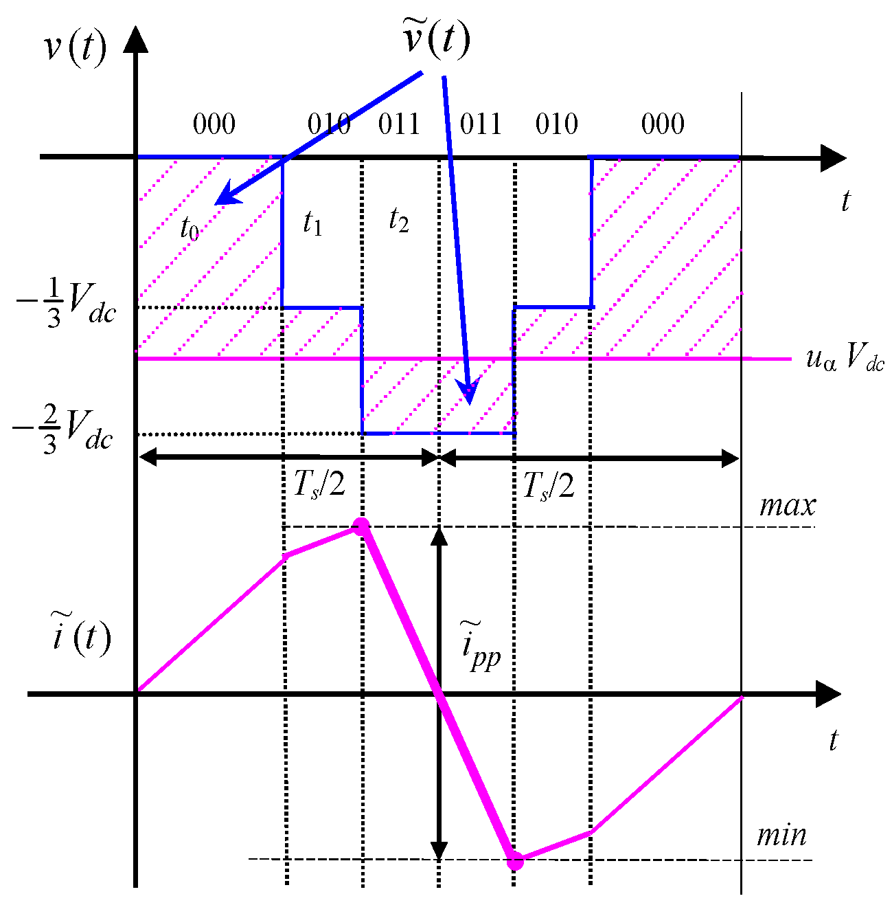
3.2.2. Evaluation of Current Ripple in Sector II

Considering sector II, 60° ≤ ϑ ≤ 120°, two different cases are considered to identify the peak-to-peak current ripple amplitude: 0 ≤ uα ≤ 1/3 and −1/3 ≤ uα ≤ 0.
The case of 0 ≤ uα ≤ 1/3 is represented in Figure 11. In this case, there are two possible values eligible for i ˜ pp , one is i ˜ pp ' given by the duty-cycle δ0 (dashed line), and the other is i ˜ pp '' determined by the duty-cycle δ2 (continuous line).
The first case (duty-cycle δ0) gives:
i ˜ pp ' = V dc T s L { u α δ 0 }
Introducing in Equation (33) the expression of δ0 given in Table 1 for sector II, the normalized current ripple becomes:
r = 2 u α ( 1 3 u β )
The second case (duty-cycle δ2) gives:
i ˜ pp '' = V dc T s L { [ u α + 1 3 ] δ 2 }
Introducing in Equation (35) the expression of δ2 given in Table 1 for sector II, the normalized current ripple becomes:
r ′′ = 3 ( u α + 1 3 ) ( 1 3 u β u α )
Comparing the two possible cases Equations (34) and (36), the normalized current ripple can be calculated by their maximum:
r = max { 2 u α ( 1 3 u β ) 3 ( u α + 1 3 ) ( 1 3 u β u α )
The case of −1/3 ≤ uα ≤ 0, the current ripple i ˜ and its peak-to-peak value i ˜ pp are depicted in Figure 12, together with the instantaneous output voltage v(t). According to Figure 12, i ˜ pp can be evaluated by Equations (1), (5), and (9), considering the duty-cycle δ2, leading to:
i ˜ pp = V dc T s L { [ 1 3 + u α ] δ 2 }
Introducing in Equation (38) the expression of δ2 given in Table 1 for sector II, the normalized current ripple becomes:
r = 3 ( u α + 1 3 ) ( 1 3 u β u α )

3.2.3. Evaluation of Current Ripple in Sector III

Considering sector III, 120° ≤ ϑ ≤ 180°, two different cases are considered to identify the peak-to-peak current ripple amplitude: −1/3 ≤ uα ≤ 0 and −1/√3 ≤ uα ≤ −1/3.
In the case −1/3 ≤ uα ≤ 0, the current ripple i ˜ and its peak-to-peak value i ˜ pp are depicted in Figure 13, together with the instantaneous output voltage v(t). According to Figure 13, i ˜ pp can be evaluated by Equations (1), (5), and (9), considering the duty-cycle δ0, leading to:
i ˜ pp = V dc T s L { u α δ 0 }
Introducing in Equation (40) the expression of δ0 given in Table 1 for sector III, the normalized current ripple becomes:
r = 2 u α + 3 u α ( 1 3 u β u α )
The case of −1/√3 ≤ uα ≤ −1/3 is depicted in Figure 14. In this case there are two possible values eligible for i ˜ pp , one is i ˜ pp ' given by the duty-cycle δ0 (continuous line), and the other is i ˜ pp '' determined by the duty-cycle δ1 (dashed line).
The first case (duty-cycle δ0) gives:
i ˜ pp ' = V dc T s L { u α δ 0 }
Introducing in Equation (42) the expression of δ0 given in Table 1 for sector III, the normalized current ripple becomes:
r = 2 u α + 3 u α ( 1 3 u β u α )
The second case (duty-cycle δ1) gives:
i ˜ pp '' = V dc T s L { [ u α + 1 3 ] δ 1 }
Introducing in Equation (44) the expression of δ1 given in Table 1 for sector III, the normalized current ripple becomes:
r ′′ = 2 3 u β [ u α + 1 3 ]
Comparing the two possible cases Equations (43) and (45), the normalized current ripple can be calculated by their maximum:
r = max { 2 u α + 3 u α ( 1 3 u β u α ) 2 3 u β [ u α + 1 3 ]

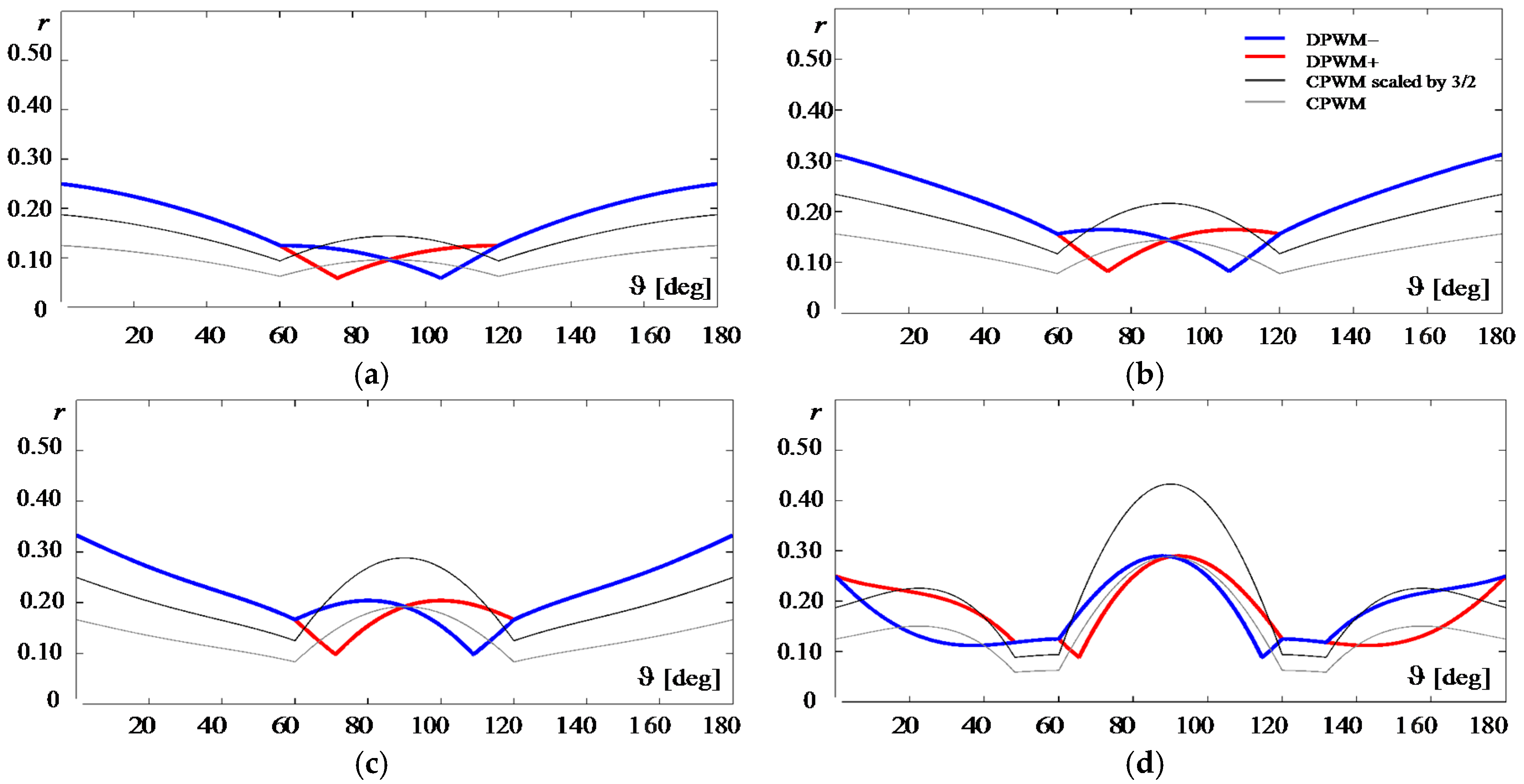
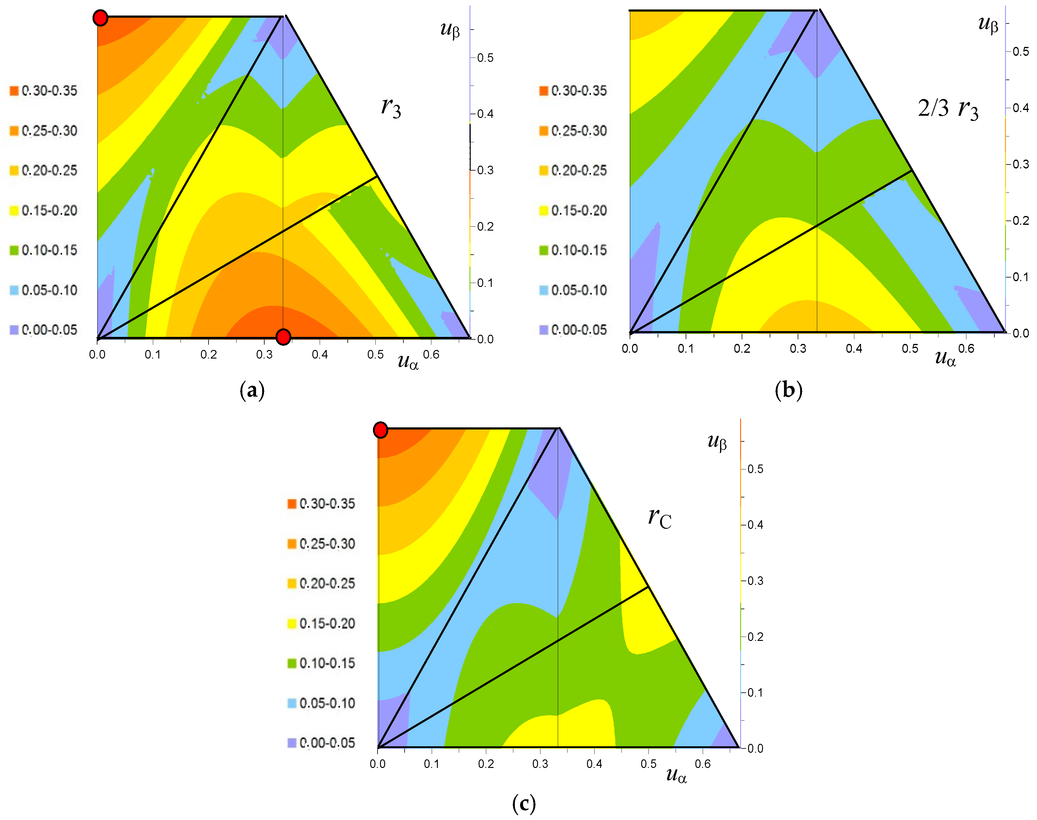
4. Ripple Diagrams and Discussion

In order to analyze and compare the current ripple distribution within the fundamental period, different kinds of diagrams are presented and discussed in this section. In particular, peak-to-peak current ripple envelopes for various modulation indexes, current ripple maps, maximum, average, and rms values of the current ripple are considered and compared for the two basic discontinuous modulations (DPWM±) and the centered (continuous) pulse-width modulation (CPWM).
Considering CPWM, that represents the optimal continuous modulation from the point of view of the current ripple amplitude and rms, reference is made to calculation and developments introduced in [18,21]. Both the cases of the same carrier frequency (fsCPWM = fsDPWM) and the same average switching frequency (fsCPWM/fsDPWM = 2/3) are considered, to account for the reduction in the number of commutations over the fundamental period in the cases of discontinuous modulation. For the evaluation of the current ripple rms, a simple method is proposed and verified, based on an approximated relation between current ripple envelope and current ripple rms.

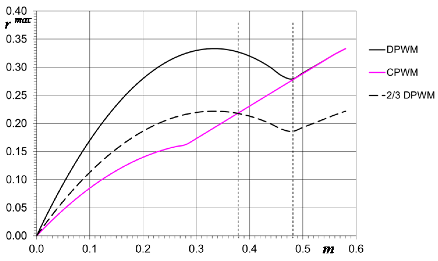
4.1. Peak-to-Peak Current Ripple Amplitude

The peak-to-peak current ripple amplitude in the cases of DPWM± and CPWM is presented in Figure 15. Considering the same carrier frequency with different modulation indexes to cover the whole linear modulation range, m = 1/6, 1/4, 1/3, and 1/2. In particular, the normalized current ripple r(m,ϑ) defined by (11) is depicted, and half of the fundamental period is considered due to the half-wave symmetry. The four traces represent the cases of DPWM− (blue trace), DPWM+ (red trace) CPWM (grey trace), and CPWM scaled by 3/2 (black trace) to account for the different average switching frequency. It can be noticed that the normalized current ripple distributions for DPWM− and DPWM+ are symmetric to each other for ϑ = 90°, i.e., r(ϑ) = r+(180°−ϑ), and r(ϑ) is symmetric to itself for ϑ = 90° in the case of CPWM (quarter-wave symmetry, as known). In general, there are intersections of r(ϑ) among the four different modulation cases, and it cannot be said that one is always better than the others. Although r(ϑ) for CPWM seems generally lower, there are wide regions in which r(ϑ) can be minimized by properly swapping between DPWM− and DPWM+ when the scaling factor 3/2 is considered to account for the same average switching frequency with CPWM.
Figure 16 shows the colored maps of the normalized current ripple r(uα, uβ) in 1st and 2nd quadrant (sectors I, II, and III in Figure 1) for the two basic discontinuous modulation techniques DPWM±, within the modulation limit (hexagon). Also in this case it is noticeable that the two maps are symmetric to each other for ϑ = 90°, i.e., r(uα, uβ) = r+(−uα, uβ). The four maps corresponding to the balanced discontinuous modulations DPWM0-3 can be easily obtained by swapping these two maps every 60°, with basic angle 0° for DPWM02, and 30° for DPWM13, according to Figure 2. Note that, starting from the half-wave symmetry of DPWM±, the balanced discontinuous modulations DPWM13 become quarter-wave symmetric in terms of current ripple.
As expected, the maps show a null current ripple corresponding to the tips of the inverter voltage vectors (including the null vector), being the output voltage perfectly corresponding to the reference voltage, with a null alternating voltage. The max of the normalized current ripple is about 0.34, emphasized with red dots in the maps of Figure 16, and corresponding to the points farther from the inverter voltage tips, i.e., rmax(uα, uβ) = r(−1/3, 0) ≈ r(0, 1/√3) ≈ r(1/3, 0) ≈ 0.34. In terms of modulation index and phase angle, positions of the maximum become: rmax(m, ϑ) = r(1/3, 180°) ≈ r(1/√3, 90°) ≈ r(1/3, 0°) ≈ 0.34.
By observing the maps and comparing with Figure 2, it is evident that the lower current ripple amplitude is obtained by combining DPWM± as for DPWM3, since it corresponds to DPWM+ for ϑ = [30°, 90°] and to DPWM− for ϑ = [90°, 150°], i.e., in the regions where the ripple is lower. This result confirms that DPWM3 is not only superior among the different DPWMs in terms of current ripple rms minimization [3], but also in terms of minimum current ripple amplitude. With similar considerations, DPWM1 can be considered as the worst DPWM, whereas DPWM± and DPWM02 are almost equivalent to each other, as it will be better shown later on.
Once the superiority of DPWM3 is established among the DPWMs, it should be compared with CPWM that is considered the optimal modulation techniques among all PWMs [4], also accounting for the different average switching frequency. For this purpose, Figure 17 shows three colored maps of the normalized current ripple r(uα, uβ) in the 1st quadrant for DPWM3 (Figure 17a), DPWM3 scaled by 2/3 (Figure 17b), and CPWM (Figure 17c). Whereas the superiority of CPWM is evident comparing to the unscaled current ripple for DPWM3, DPWM3 becomes better than CPWM if the scaling by 2/3 is considered for the current ripple. In particular, it is well visible that the two regions appearing red (normalized ripple 0.3–0.35) in Figure 17a turn to orange (normalized ripple 0.2–0.25) in Figure 17b, leading to two normalized current ripple maxima around 0.22, comparing to the single maximum around 0.34 (red dot in Figure 17c) in case of CPWM.
Generally speaking, it can be noted that both the basic discontinuous modulations DPWM± and the centered modulation CPWM do not show any discontinuity of the current ripple amplitude distribution within the fundamental period, whereas the balanced discontinuous modulations DPWM0-3 do, caused by the swapping between DPWM− and DPWM+ every 60°. Obviously, there are discontinuities only if the ripple amplitudes for DPWM− and DPWM+ are different corresponding to the specific swap angle. In Figure 17a a discontinuity can be observed at 30° only in case of high modulation index, being the current ripple amplitude practically the same for DPWM− and DPWM+ for low modulation index (i.e., m ≤ 0.4), as shown in Figure 15 and Figure 16.

4.2. Maximum of the Current Ripple

In order to have a first estimation of the current ripple amplitude in the case of DPWMs, the maximum of the current ripple over the whole fundamental period is evaluated as function of the modulation index. For this purpose, reference is made to the position of the red dots in Figure 16. It can be noticed that the two local maxima are located along the directions ϑ = 0° and ϑ = 90° for all the DPWM cases. To determine these local maxima, uα = m, uβ = 0 can be set in Equation (30), and uα = 0, uβ = m can be set in Equation (37), leading to the following global maximum:
r max ( m ) = max { m ( 2 3 m ) ,   1 3 m }
The intersection between the two local maxima gives the border value of modulation index:
m ( 2 3 m ) = 1 3 m
leading to m ≈ 0.474. Finally, combining Equations (47) and (48), maximum of normalized current ripple is:
r max ( m ) = { m ( 2 3 m ) for   m     0.474 , 1 3 m for   m     0.474
In Figure 18, the maximum value of the normalized current ripple Equation (49) (continuous black trace) as a function of the modulation index, valid for all the considered DPWMs is presented, which is also scaled by 2/3 (dashed black trace) and compared to the case of CPWM (pink trace), already developed in [18,21]. It can be noted that the maximum ripple in the case of CPWM is lower compared to the case of DPWM for low-medium modulation indexes, up to 0.474. For m ≥ 0.474, CPWM and DPWM give the same maximum current ripple. When considering the same average switching frequency, i.e., scaling by 2/3, the maximum ripple in case of DPWM becomes lower than in the case of CPWM for m ≥ 0.378. The approximation of maximum current ripple almost proportional to modulation index, valid for the case of CPWM over the whole modulation range [18], does not apply to the DPWM.

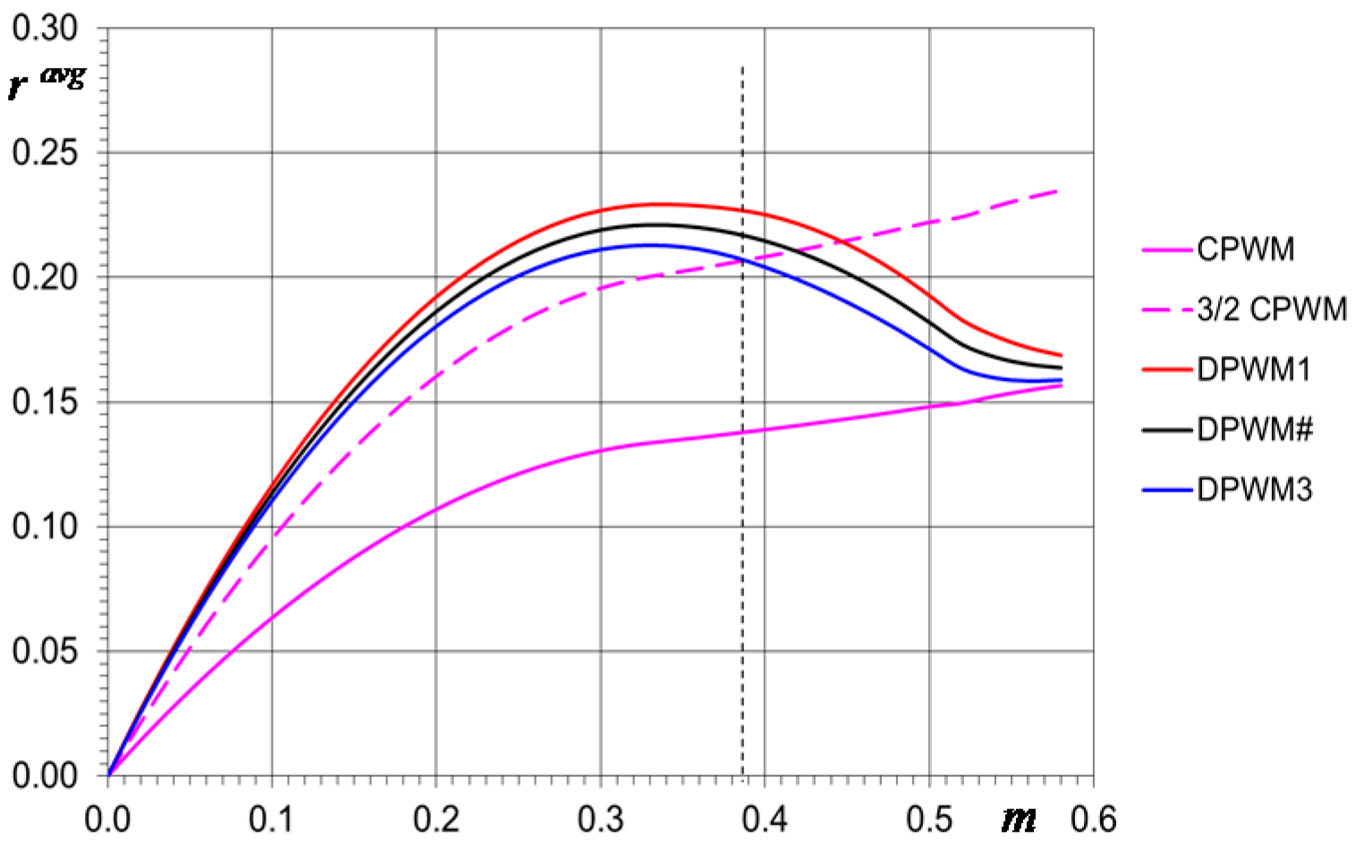
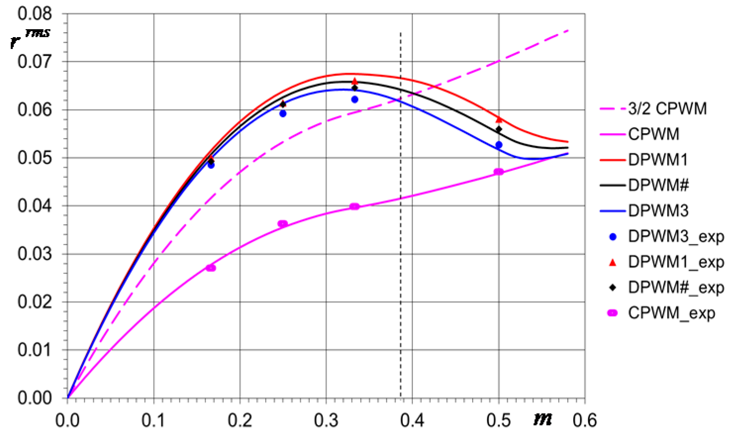
4.3. Average Peak-to-Peak Current Ripple

In order to summarize the current ripple amplitude over the whole fundamental period, the normalized ripple average ravg is introduced in Figure 19 as a function of the modulation index. All the previously considered modulation techniques are analyzed: DPWM# (including the four cases DPWM± and DPWM02), DPWM1, DPWM3, CPWM, and CPWM scaled by 3/2.
The case of CPWM shows the minimum average current ripple over the whole modulation range, whereas DPWM3 and DPWM1 present the minimum and the maximum ravg among the different DPWMs, respectively. The four cases DPWM± and DPWM02 are perfectly equivalent (DPWM#), as recognizable comparing the maps of Figure 16 to Figure 2.
By considering the same average switching frequency, i.e., scaling the case of CPWM by 3/2 (dashed line in Figure 19), it is confirmed that DPWMs offers a lower (average) current ripple comparing to CPWM for high modulation indexes. In particular, the case of DPWM3 presents a lower (average) ripple for m ≥ 0.38 (approximately) comparing to the case of CPWM, which is the same result obtained when the maximum of the current ripple is considered (Figure 18).
The above results lead to consider DPWMs, and in particular DPWM3, superior to CPWM in terms of minimization of current ripple amplitude for high modulation indexes, i.e., higher than ≈0.38. This is the case of grid-connected applications, where the modulation index is always ranging around the maximum, corresponding to the grid voltage amplitude that is almost constant.

4.4. Relation Between Peak-to-Peak and Current Ripple Rms

The knowledge of the peak-to-peak current ripple amplitude distribution over the fundamental period can be also used for the estimation of the current ripple rms. In particular, the instantaneous current ripple can be approximated by a triangular waveform, modulated by the ripple amplitude, and the rms of the resulting modulated triangular waveform can be readily determined, being the rms of a triangular waveform simply calculated by dividing its peak value by 3 .
In this way, the approximated current ripple rms over the switching period Ts becomes:
i ˜ rms ( T s ) 1 3 i ˜ pp 2
Considering the rms over the whole fundamental period and normalizing, Equation (50) becomes:
r rms ( T ) = 2 L V dc T s i ˜ rms ( T ) 1 2 3 rms { r ( T ) }
An example is given in Figure 20: Figure 20a shows the instantaneous current ripple (simulated) with its envelope, as determined in Section 3. Figure 20b shows a triangular waveform modulated by the same envelope of Figure 20a. This example has been carried out by a Matlab-Simulink simulation considering Vdc = 300 V, fs = 1/Ts = 3 kHz, m = 1/3, f = 1/T = 50 Hz, 3-phase VSI, passive load R = 10 Ω, L = 18 mH, in the case of DPWM+. In this case, the rms of the instantaneous current ripple results in 0.1878 A, whereas the rms of the modulated triangular waveform is 0.1896 A, with a mismatch lower than 1%. It has been verified by numerical simulations that the rms estimation error is always in the order of few % for all the modulation techniques, over the whole modulation range. In general, this method overestimates the current ripple rms, since the real peak-to-peak current behavior is approximated by straight lines (triangular waveform), corresponding to two output voltage levels instead of three.
The normalized current ripple rms calculated according to Equation (51) in case of CPWM and DPWMs are shown in Figure 21, confirming the superiority of DPWMs comparing to CPWM for high modulation indexes, also in terms of current ripple rms. The simplified rms calculation presented in Figure 21 can be compared with the corresponding diagrams existing in literature, and in particular considering Figure 13 in [3], Figure 6 in [5], Figure 7 in [10], and Figure 10 in [6], showing a satisfactory matching.

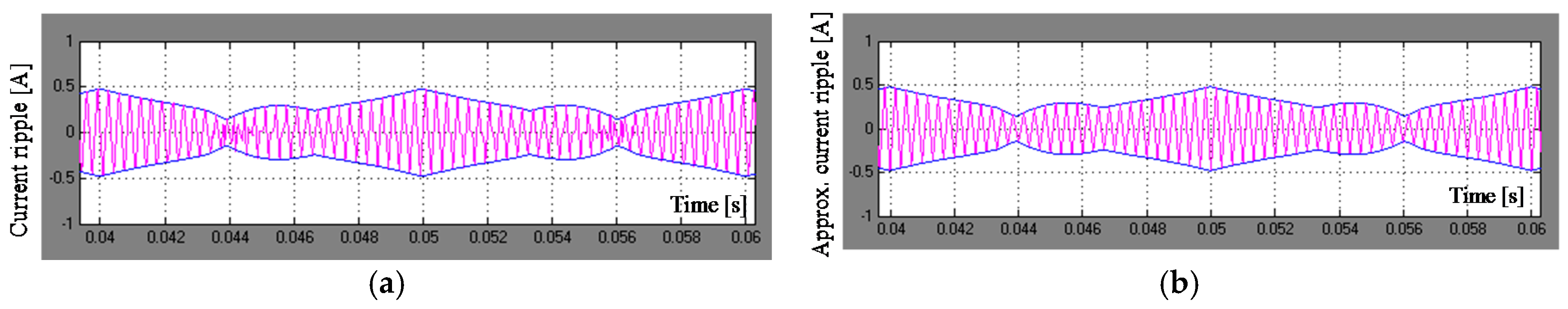
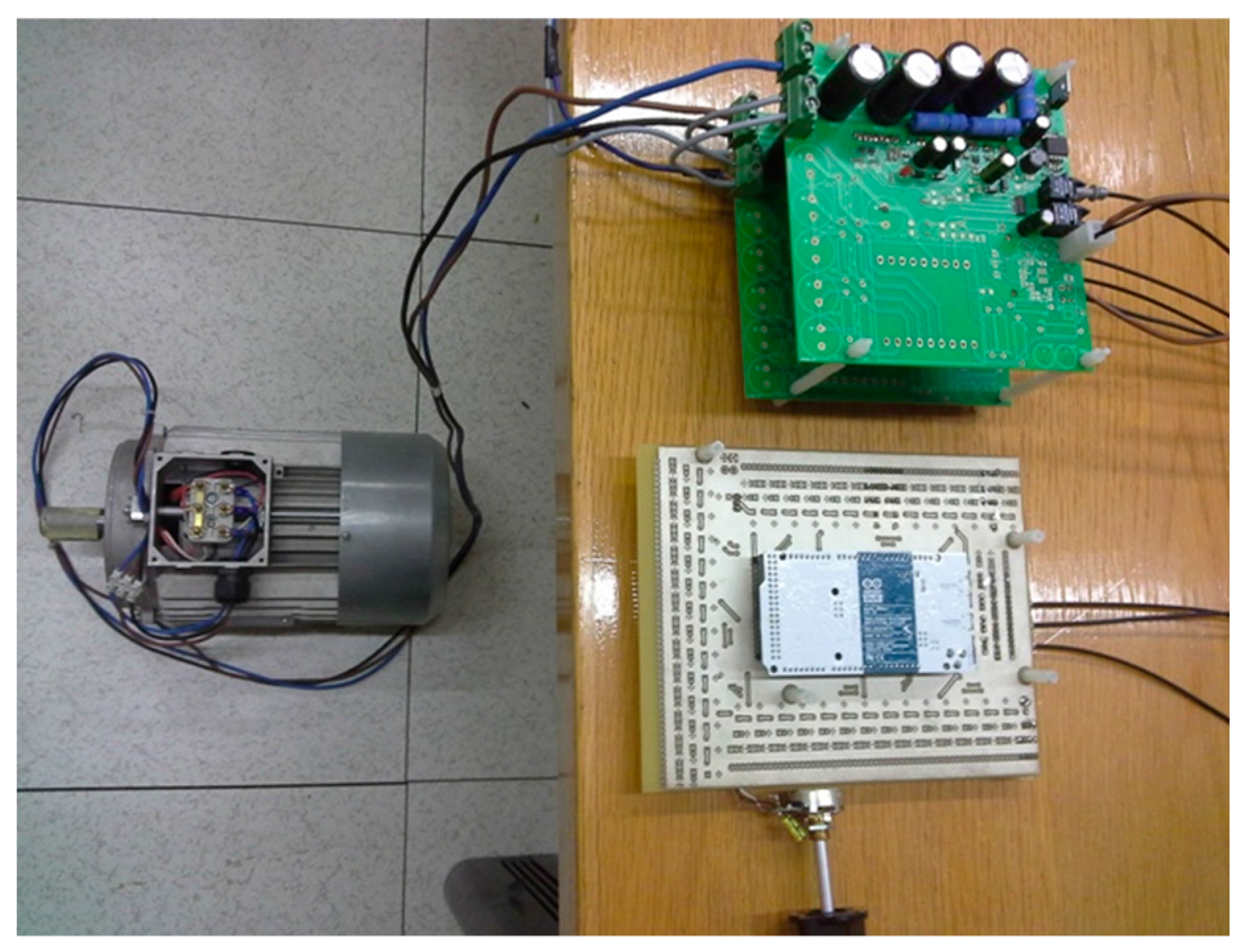
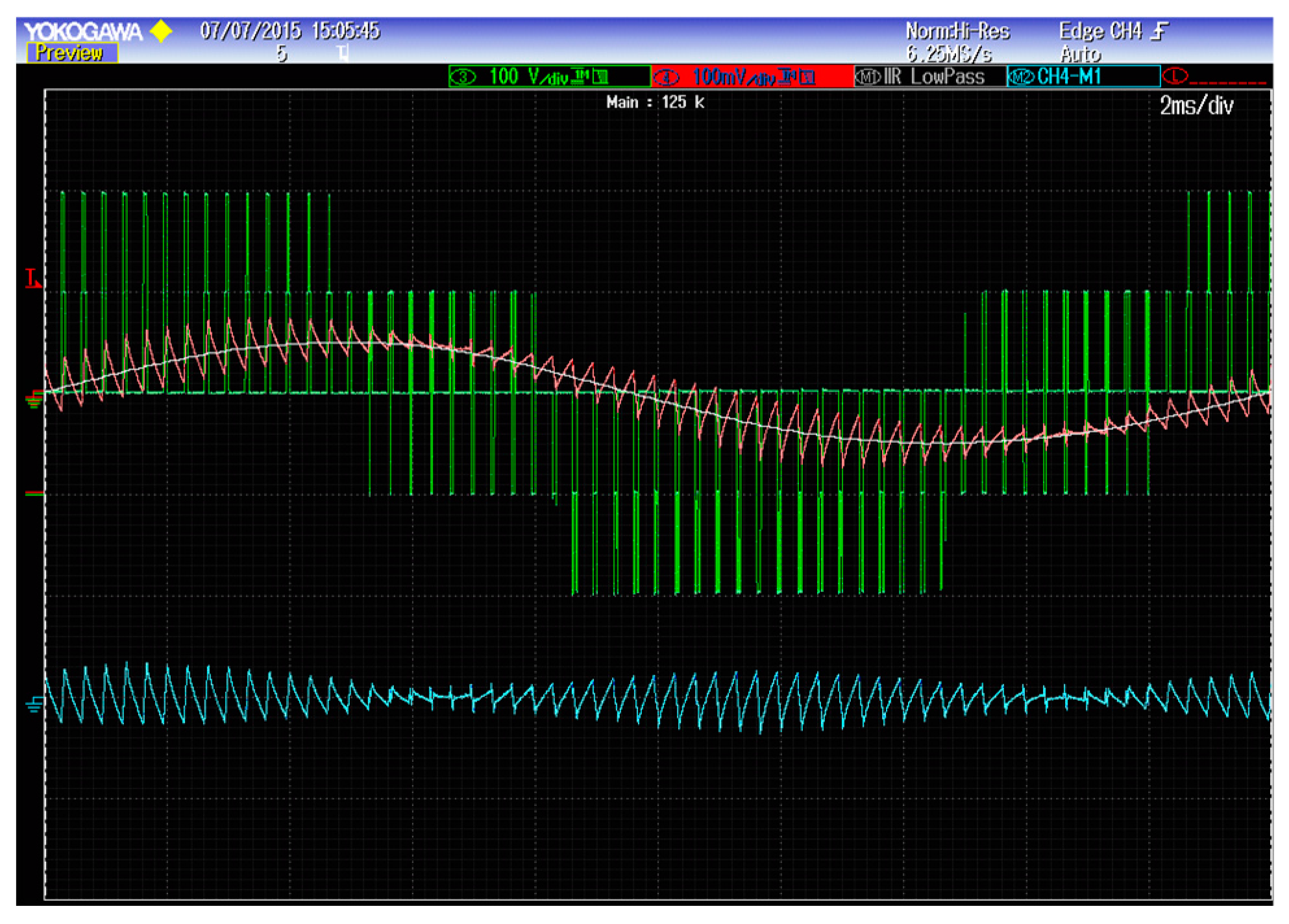
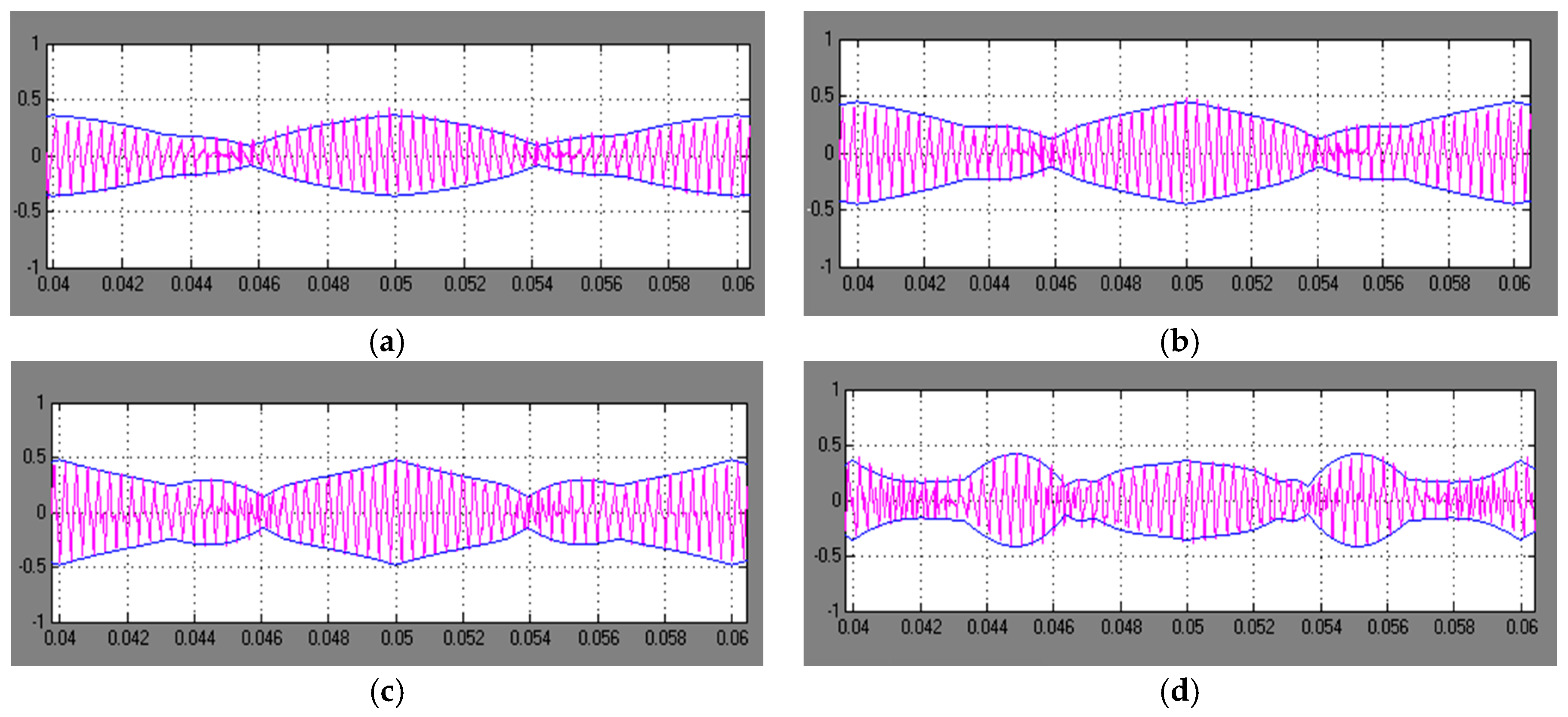
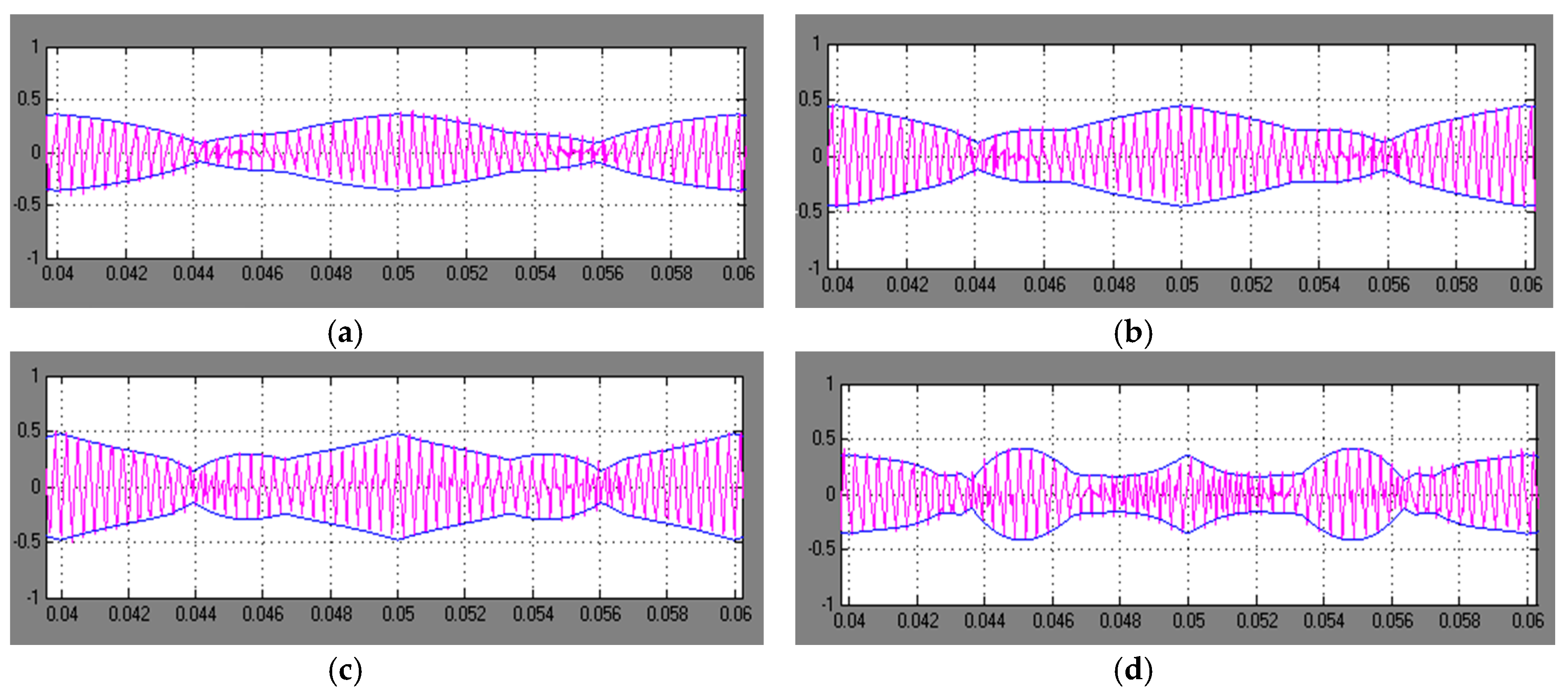
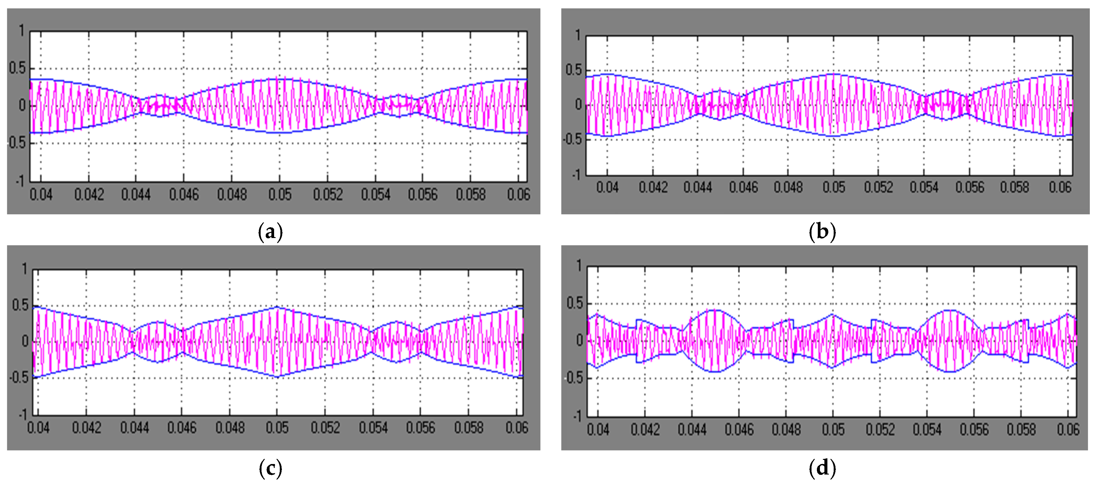
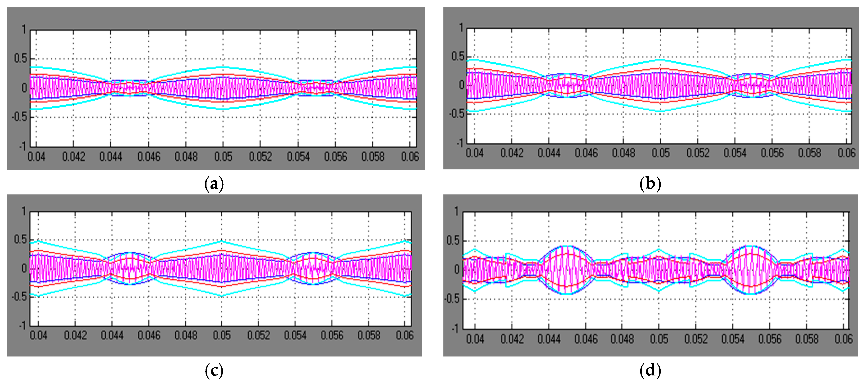
5. Experimental Results

Experimental results have been carried out in order to verify theoretical developments for all considered PWM techniques. The experimental setup consists of the custom-made three-phase inverter controlled by the Arduino Due microcontroller board, based on the 84 MHz Atmel SAM3X8E ARM Cortex-M3 CPU. The experimental setup is presented in Figure 22. The three-phase PS22A76 intelligent power module (1200 V, 25 A, Mitsubishi Electric Corporation, Tokyo, Japan) has been used for the implementation of the three-phase inverter. The experiments have been carried out by supplying a star-connected induction motor with the following rated parameters: Pn = 2.2 kW, Vn = 380 V, In = 5.2 A and fn = 50 Hz. According to the high-frequency model of induction motors, only the total equivalent leakage inductance L is taken into account for the current ripple estimation. It has been experimentally estimated to be L ≈ 18 mH (in the switching frequency range).
The three-phase inverter has been supplied by the dc-link voltage Vdc = 300 V. The switching frequency has been set to fs = 1/Ts = 3 kHz and the fundamental frequency has been kept at f = 1/T = 50 Hz for easier comparison with analytical developments. A relatively low switching frequency has been chosen in order to keep the current ripple clearly visible within a fundamental period. The Yokogawa DLM2024 oscilloscope (Yokogawa Electric Corporation, Tokyo, Japan), with the PICO TA057 differential voltage probe (Tyler, TX, USA) and LEM PR30 current probe (LEM Europe GmbH, Fribourg, Switzerland), has been used for all measurements. The current ripple i ˜ ( t ) has been estimated using the oscilloscope’s mathematical functions by subtracting the fundamental current component from the instantaneous current (as for the blue trace in Figure 23), and it has been uploaded in the workspace of Matlab to be compared to the theoretical ripple envelopes.
An example of the system behavior is given in Figure 23, considering the case of DPWM3 with m = 1/6: Pole-to-neutral voltage (green trace), instantaneous current (red trace), fundamental current component (grey trace), and current ripple (blue trace), for one fundamental period (20 ms).
In Figure 24, Figure 25, Figure 26 and Figure 27, experimental current ripples (pink traces) and envelopes (blue traces) for the four relevant modulation cases are presented. In particular, the investigated PWM techniques are the basic positive and negative clamped discontinues modulation, i.e., DPWM± (Figure 24 and Figure 25), the optimal discontinues modulation, i.e., DPWM3 (Figure 26), and the optimal continuous modulation (centered), i.e., CPWM (Figure 27). For each one of these modulation techniques, different modulation indexes are considered: m = 1/6, 1/4, 1/3 and 1/2.
The experimental current ripples match the theoretical envelops in a very satisfactory way for all the considered cases, confirming the effectiveness of the proposed analytical developments.
In order to underline the comparison between the best discontinuous and continuous modulation techniques, in addition to the current envelope for CPWM (blue trace) calculated as in [18,21], in Figure 27 the current envelope of DPWM3 (turquoise trace) and its value scaled by 2/3 (red trace) to account for the different average switching frequency is also presented.
It can be inferred that current ripple in case of CPWM is generally lower than in case of DPWM3, but DPWM3 becomes equivalent or even better than CPWM (for high modulation index) when the scale factor 2/3 is applied to consider the same average switching frequency, confirming the considerations given in previous sections.
Finally, the simplified method proposed in Section 4.4. for evaluating the current ripple rms on the basis of the ripple envelope has been experimentally verified in all cases of CPWM and DPWMs techniques, for different modulation indexes. In particular, the experimental current ripple rms calculated by the scope (rms of the blue trace in Figure 23) are presented with dots in the previous Figure 21, corresponding to m = 1/6, 1/4, 1/3 and 1/2. Matching with the values approximated by Equation (51) is generally good, with a resolution in the order of few percent, confirming the effectiveness of the simplified proposed method.

6. Conclusions

The output current ripple in three-phase inverters for the different discontinuous PWM techniques has been analytically calculated and compared in this paper. In particular, the expression of peak-to-peak current ripple amplitude has been derived over the whole fundamental period as function of the modulation index. The normalized current ripple has been introduced and different ripple maps and diagrams have been investigated, making possible a comparison with centered PWM, considered as the optimal continuous modulation.
In particular, maps of normalized current ripple have been carried out for positive and negative clamped discontinuous modulations (DPWM+ and DPWM−) in the output voltage space vector plane. The maps for all the other balanced discontinuous modulation techniques (DPWM0, DPWM1, DPWM2, and DPWM3) can be easily carried out by combining the 60° sectors of these two basic maps. The diagrams with maximum, average, and rms of the current ripple amplitude have been presented. It has been pointed out that the maximum peak-to-peak current ripple amplitude is almost proportional with the modulation index for CPWM technique, while for all the different DPWM techniques it has exactly the same parabolic behavior, reaching one absolute maximum around m = 1/3. With reference to the average current ripple, DPWM3 shows the better behavior among all the DPWM techniques, whereas DPWM1 is the worst case. Both the maximum and the average current ripples of all DPWM techniques are higher compared to the CPWM, over the whole modulation range. However, if the scale factor 3/2 is introduced to account for the different average switching frequency between CPWM and DPWMs, the current ripple amplitude becomes lower for DPWM3 compared to CPWM for high modulation indexes, i.e., for m > 0.38. This result suggests the use of DPWM3 in case of grid-connected application, where the output inverter voltage amplitude is always similar to the (constant) grid voltage amplitude, with a modulation index always ranging near to its maximum if the inverter is properly designed.
The analytical developments have been experimentally verified for all the relevant DPWM techniques, considering various modulation indexes. The results show a very good match between the measured current ripple and theoretical envelopes, proving the correctness and effectiveness of the proposed analysis.
Additionally, a simple approximated method to correlate the calculated current ripple envelope with the current ripple rms has been proposed and experimentally verified for all the DPWMs and CPWM techniques. This method can be considered as a viable alternative solution to evaluate the current ripple rms compared to the other methods available in literature.

Author Contributions

All the contributions in this paper are equally shared among the authors Gabriele Grandi, Jelena Loncarski, and Milan Srndovic.

Conflicts of Interest

The authors declare no conflict of interest.

References

  1. Van der Broeck, H.W.; Skudelny, H.-C.; Stanke, G.V. Analysis and realization of a pulse width modulator based on voltage space vectors. IEEE Trans. Ind. Appl. 1988, 24, 142–150. [Google Scholar] [CrossRef]
  2. Hava, A.M.; Kerkman, R.J.; Lipo, T.A. Carrier-Based PWM-VSI Overmodulation strategies: Analysis, comparison, and design. IEEE Trans. Power Electron. 1998, 13, 674–689. [Google Scholar] [CrossRef]
  3. Hava, A.M.; Kerkman, R.J.; Lipo, T.A. Simple analytical and graphical methods for carier-based PWM-VSI drives. IEEE Trans. Power Electron. 1999, 14, 49–61. [Google Scholar] [CrossRef]
  4. Holmes, G.D.; Lipo, T.A. Pulse width modulation for power converters: Principles and practice. In IEEE Press Series on Power Engineering; John Wiley & Sons: Oxford, UK, 2003. [Google Scholar]
  5. Kolar, J.W.; Ertl, H.; Zach, F.C. Influence of the modulation method on the conduction and switching losses of a PWM converter system. IEEE Trans. Ind. Appl. 1991, 27, 1063–1075. [Google Scholar] [CrossRef]
  6. Casadei, D.; Serra, G.; Tani, A.; Zarri, L. Theoretical and experimental analysis for the RMS current ripple minimization in induction motor drives controlled by SVM technique. IEEE Trans. Ind. Electron. 2004, 51, 1056–1065. [Google Scholar] [CrossRef]
  7. Holtz, J. Pulsewidth modulation for electric power conversion. IEEE Proc. 1994, 82, 1194–1214. [Google Scholar] [CrossRef]
  8. Depenbrock, M. Pulse Width Control of a 3-Phase Inverter with Nonsinusoidal Phase Voltages. In Proceedings of the IEEE International Semiconductor Power Converter Conference Record, New York, NY, USA, 1977; pp. 399–403.
  9. Ogasawara, S.; Nabae, A.; Akagi, H. A novel PWM scheme of voltage source inverter based on space vector theory. Arch. Elektrotech. 1990, 74, 33–41. [Google Scholar] [CrossRef]
  10. Hava, A.M.; Kerkman, R.J.; Lipo, T.A. A high-performance generalized discontinuous PWM algorithm. IEEE Trans. Ind. Appl. 1998, 34, 1059–1071. [Google Scholar] [CrossRef]
  11. Ojo, O. The generalized discontinuous PWM scheme for three-phase voltage source inverters. IEEE Trans. Ind. Electron. 2004, 51, 1280–1289. [Google Scholar] [CrossRef]
  12. Beig, A.R.; Kanukollu, S.; Hosani, K.A.; Dekka, A. Space-vector-based synchronized three-level discontinuous PWM for medium-voltage high-power VSI. IEEE Trans. Ind. Electron. 2014, 61, 3891–3901. [Google Scholar] [CrossRef]
  13. Sekhar, K.R.; Srinivas, S. Discontinuous decoupled PWMs for reduced current ripple in a dual two-level inverter fed open-end winding induction motor drive. IEEE Trans. Power Electron. 2013, 28, 2493–2502. [Google Scholar] [CrossRef]
  14. Charumit, C.; Kinnares, V. Discontinuous SVPWM techniques of three-leg VSI-fed balanced Two-phase loads for reduced switching losses and current ripple. IEEE Trans. Power Electron. 2015, 30, 2191–2204. [Google Scholar] [CrossRef]
  15. Dujic, D.; Jones, M.; Levi, E. Analysis of output current ripple rms in multiphase drives using space vector approach. IEEE Trans. Power Electron. 2009, 24, 1926–1938. [Google Scholar] [CrossRef]
  16. Dujic, D.; Jones, M.; Levi, E.; Prieto, J.; Barrero, F. Switching ripple characteristics of space vector PWM schemes for five-phase two-level voltage source inverters—Part 2: Flux harmonic distortion factors. IEEE Trans. Ind. Electron. 2011, 58, 2789–2808. [Google Scholar] [CrossRef]
  17. Ruderman, A.; Wang, F. Understanding PWM current ripple in star-connected AC motor drive. IEEE Power Electron. Soc. Newsl. 2009, 21, 14–17. [Google Scholar]
  18. Grandi, G.; Loncarski, J. Evaluation of Current Ripple Amplitude in Three-Phase PWM Voltage Source Inverters. In Proceedings of the 8th International Conference on Compatibility Power Electronics, Ljubljana, Slovenia, 5–7 June 2013; pp. 156–161.
  19. Park, J.-H.; Jeong, H.-G.; Lee, K.-B. Output current ripple reduction algorithms for home energy storage systems. Energies 2013, 6, 5552–5569. [Google Scholar] [CrossRef]
  20. Jiang, D.; Wang, F. Current-ripple prediction for three-phase PWM converters. IEEE Trans. Ind. Appl. 2014, 50, 531–538. [Google Scholar] [CrossRef]
  21. Grandi, G.; Loncarski, J.; Dordevic, O. Analysis and comparison of peak-to-peak current ripple in two-level and multilevel PWM inverters. IEEE Trans. Ind. Electron. 2015, 62, 2721–2730. [Google Scholar] [CrossRef]
  22. Loncarski, J.; Leijon, M.; Srndovic, M.; Rossi, C.; Grandi, G. Comparison of output current ripple in single and dual three-phase inverters for electric vehicle motor drives. Energies 2015, 8, 3832–3848. [Google Scholar] [CrossRef]
  23. Grandi, G.; Loncarski, J. Analysis of peak-to-peak current ripple amplitude in seven-phase PWM voltage source inverters. Energies 2013, 6, 4429–4447. [Google Scholar] [CrossRef]
  24. Lewicki, A. Dead-time effect compensation based on additional phase current measurements. IEEE Trans. Ind. Electron. 2015, 62, 4078–4085. [Google Scholar] [CrossRef]
  25. Grandi, G.; Loncarski, J.; Seebacher, R. Effects of Current Ripple on Dead-Time Distortion in Three-Phase Voltage Source Inverters. In Proceedings of the 2012 IEEE International Energy Conferences and Exhibition, Florence, Italy, 9–12 September 2012; pp. 207–212.
  26. Wu, F.; Feng, F.; Luo, L.; Duan, J.; Sun, L. Sampling period online adjusting-based hysteresis current control without band with constant switching frequency. IEEE Trans. Ind. Electron. 2015, 62, 270–277. [Google Scholar] [CrossRef]
  27. Jiang, D.; Wang, F.F. Variable switching frequency PWM for three-phase converters based on current ripple prediction. IEEE Trans. Power Electron. 2013, 28, 4951–4931. [Google Scholar] [CrossRef]
  28. Asiminoaei, L.; Rodriguez, P.; Blaabjerg, F.; Malinowski, M. Reduction of switching losses in active power filters with a new generalized discontinuous-PWM strategy. IEEE Trans. Ind. Electron. 2008, 55, 467–471. [Google Scholar] [CrossRef]
Figure 1. Output voltage space vector diagram and sectors (normalized by Vdc).
Energies 09 00380 g001
Figure 2. Distribution of zero switching states in balanced discontinuous pulse-width modulations (DPWMs): (a) inner: DPWM0 and outer: DPWM2; and (b) inner: DPWM1 and outer: DPWM3.
Energies 09 00380 g002
Figure 3. Output voltage and current ripple for DPWM− technique in one switching period (sector I, 0 ≤ uα ≤ 1/3).
Energies 09 00380 g003
Figure 4. Output voltage and current ripple for DPWM− technique in one switching period (sector I, uα ≥ 1/3).
Energies 09 00380 g004
Figure 5. Output voltage and current ripple for DPWM− technique in one switching period (sector II, 0 ≤ uα ≤ 1/3).
Energies 09 00380 g005
Figure 6. Output voltage and current ripple for DPWM− technique in one switching period (sector II, −1/3 ≤ uα ≤ 0).
Energies 09 00380 g006
Figure 7. Output voltage and current ripple for DPWM− technique in one switching period (sector III, −1/3 ≤ uα ≤ 0).
Energies 09 00380 g007
Figure 8. Output voltage and current ripple for DPWM− technique in one switching period (sector III, uα ≤ −1/3).
Energies 09 00380 g008
Figure 9. Output voltage and current ripple for DPWM+ technique in one switching period (sector I, 0 ≤ uα ≤ 1/3).
Energies 09 00380 g009
Figure 10. Output voltage and current ripple for DPWM+ technique in one switching period (sector I, uα ≥ 1/3).
Energies 09 00380 g010
Figure 11. Output voltage and current ripple for DPWM+ technique in one switching period (sector II, 0 ≤ uα ≤ 1/3).
Energies 09 00380 g011
Figure 12. Output voltage and current ripple for DPWM+ technique in one switching period (sector II, −1/3 ≤ uα ≤ 0).
Energies 09 00380 g012
Figure 13. Output voltage and current ripple for DPWM+ technique in one switching period (sector III, −1/3 ≤ uα ≤ 0).
Energies 09 00380 g013
Figure 14. Output voltage and current ripple for DPWM+ technique in one switching period (sector III, −1/√3 ≤ uα ≤ −1/3).
Energies 09 00380 g014
Figure 15. Normalized peak-to-peak current ripple amplitude r(m,ϑ) over the range ϑ = [0, 180°] in case of DPWM− (blue trace), DPWM+ (red trace), centered pulse-width modulation (CPWM) (grey trace) and CPWM scaled by 3/2 (black trace), for different modulation indexes: (a) m = 1/6; (b) m = 1/4; (c) m = 1/3; and (d) m = 1/2.
Energies 09 00380 g015
Figure 16. Maps of normalized current ripple in the normalized output voltage plane: (a) negative clamped, DPWM−; and (b) positive clamped, DPWM+. The maxima of the ripple are emphasized with red dots.
Energies 09 00380 g016
Figure 17. Maps of normalized current ripple in the normalized output voltage plane: (a) DPWM3; (b) DPWM3 scaled by 2/3; and (c) CPWM.
Energies 09 00380 g017
Figure 18. Maximum of normalized peak-to-peak current ripple as the function of modulation index for different modulation techniques.
Energies 09 00380 g018
Figure 19. Average of the normalized peak-to-peak current ripple as the function of modulation index for different modulation techniques.
Energies 09 00380 g019
Figure 20. Approximation to evaluate current ripple rms in the example case of DPWM+, m = 1/3: (a) instantaneous ripple (simulated, pink trace) with calculated envelope (blue trace); and (b) pure triangular waveform modulated by the same calculated envelope.
Energies 09 00380 g020
Figure 21. Approximated normalized current ripple rms (lines) compared to the experimental results (dots) for DPWM and CPWM techniques
Energies 09 00380 g021
Figure 22. Experimental setup: Induction motor (left) supplied by three-phase inverter (top) and microcontroller board (bottom).
Energies 09 00380 g022
Figure 23. Details of line-to-neutral voltage, instantaneous current, fundamental current, and current ripple for DPWM3, m = 1/6.
Energies 09 00380 g023
Figure 24. Experimental current ripple and theoretical envelope in the case of DPWM− for: (a) m = 1/6; (b) m = 1/4; (c) m = 1/3; and (d) m = 1/2.
Energies 09 00380 g024
Figure 25. Experimental current ripple and theoretical envelope in the case of DPWM+ for: (a) m = 1/6; (b) m = 1/4; (c) m = 1/3; and (d) m = 1/2.
Energies 09 00380 g025
Figure 26. Experimental current ripple and theoretical envelope in the case of DPWM3 for: (a) m = 1/6; (b) m = 1/4; (c) m = 1/3; and (d) m = 1/2.
Energies 09 00380 g026
Figure 27. Experimental current ripple and theoretical envelope in the case of CPWM for: (a) m = 1/6; (b) m = 1/4; (c) m = 1/3; and (d) m = 1/2.
Energies 09 00380 g027
Table 1. Duty cycles calculated in half fundamental period.
Sectorδ1δ2δ0
I 3 2 ( u α 1 3 u β ) 3 u β 1 3 2 ( u α + 1 3 u β )
II 3 2 ( u α + 1 3 u β ) 3 2 ( 1 3 u β u α ) 1 3 u β
III 3 u β 3 2 ( u α 1 3 u β ) 1 3 2 ( 1 3 u β u α )

