Review

One-Dimensional TiO2 Nanostructured Photoanodes: From Dye-Sensitised Solar Cells to Perovskite Solar Cells

1
Nanomaterials Centre, Australian Institute for Bioengineering and Nanotechnology (AIBN), School of Chemical Engineering, The University of Queensland, St. Lucia, QLD 4027, Australia
2
Particles and Catalysis Research Group, School of Chemical Engineering, The University of New South Wales, Sydney, NSW 2052, Australia
*
Authors to whom correspondence should be addressed.
Energies 2016, 9(12), 1030; https://doi.org/10.3390/en9121030
Submission received: 16 September 2016 / Revised: 18 November 2016 / Accepted: 28 November 2016 / Published: 6 December 2016
(This article belongs to the Special Issue Selected Papers from 2nd Energy Future Conference)

Abstract

:
This review presents one dimensional (1D) TiO2 nanostructured photoanodes for next generation solar cells such as dye-sensitised solar cells (DSCs) and perovskite solar cells (PSCs). Due to the unique morphological properties, 1D TiO2 nanostructures can act as express electron channels as well as light scattering layer, leading to improved charge transport properties, such as charge separation, electron injection, and electron lifetime, and light harvesting efficiency. As 1D TiO2 nanostructures are applied to solar cells, 1D TiO2 nanostructures should be further modified to overcome some drawbacks. In this review, we have described some solutions by introducing various 1D TiO2 synthetic methods and device fabrication processes for solar cell applications, where we have described some important surface engineering and hierarchical device design strategies that facilitate charge transport and light utilisation in 1D TiO2 nanostructured photoanode system.

1. Introduction

To address the global concerns about the energy crisis and environmental issues, one of the most promising solutions is the utilisation of solar energy. Solar energy is an abundant and free energy source, which can offer an amount of energy equivalent to that consumed by the whole world’s population in an entire year through just 90 min-irradiation on the surfaces of the Earth [1]. Solar cells would be one of the commercially available approaches to make a good use of solar energy. In addition, due to the sustainability and cleanliness of solar cells, it has attracted great attention as the key green technology to replace fossil fuel energy-based technologies. Basically, the energy conversion from the sunlight to the electricity on solar cells is driven by electron-hole charge separation and transfer processes, occurring at semiconducting materials with suitable bandgap energy under the sunlight. The key technology of solar cells is closely related with the development of semiconducting photovoltaic materials, and thus current studies on solar cells are focusing on high efficiency solar cells using low-cost semiconducting photovoltaic materials as an alternative to Si-based solar cells requiring expensive processes and materials. In particular, due to the use of low-cost materials and simple fabrication processes, relatively high efficiency, and the possibility of making flexible/wearable devices, dye-sensitised solar cells (DSCs) and perovskite solar cells (PSCs) are of great interest as the alternative next generation solar cells. In 1980, Matsumura et al. [2] first reported the basic idea of dye sensitization and surface semiconductor electrodes where the power conversion efficiency (PCE) of the reported DSCs with Rose Bengal dye was 2.5%. The current design of DSCs was proposed by O’Regan and Gratzel in 1991 [3], which provided a starting platform in further developing high efficiency DSCs, and this has led to the development of PSCs, based on the architecture of solid-state DSCs. The development progress of PSCs shows an amazing breakthrough in a short period of time since the original work on PSCs was first reported by Kojima et al. in 2009 [4]. Up to now, the certified best PCE of PSCs is 22.1%, which is comparable to those of high efficiency thin film solar cells such as Si-, CuInGaSe2- and CdTe-based solar cells [5]. Interestingly, the working mechanism and device structure of the recently developed PSCs are very similar to those of DSCs, and it is particularly important to note that the use of TiO2 in both solar cells is critical to achieve high performance [6]. In fact, TiO2 is a versatile semiconducting material that has widely been used in photocatalytic applications associated with energy and environmental research fields [7,8,9,10,11]. In DSCs and PSCs, thin and compact TiO2 blocking layers added onto the conductive substrates act as an electron transport layer (ETL) by efficiently separating and transferring charges because the conduction and valence band positions of TiO2, interfacing with the active semiconducting layers, are ideal to selectively transfer electrons and block holes, generated from the active layers including dyes or perovskites as a sensitiser. In addition to TiO2 blocking layers, mesoporous TiO2 active layers provide a scaffold to adsorb the large amount of sensitisers so that overall light harvesting efficiency of solar cells can be improved, followed by increasing photocurrent density. Therefore optimising TiO2 layers as a photoanode material in DSCs and PSCs has been extensively studied to achieve high efficiency solar cells, and therein controlling crystallinity, thickness, and morphology of TiO2 layers has been mainly considered [6,12].
In the past few years, one-dimensional (1D) TiO2 nanostructured materials have continuously been investigated as the photoanode materials for DSCs. The unique morphology and novel properties of 1D TiO2 nanostructured materials lead to improved photovoltaic performance in DSC systems by the excellent charge separation, fast charge injection, and efficient light utilisation, whereas trap sites existing in the randomly oriented mesoporous TiO2 structure result in charge recombination, which is one of the main reasons for poor photovoltaic performances [13,14]. Like 1D TiO2 nanostructures, 1D ZnO nanostructures also provide good charge transport properties with high crystallinity under low temperature processes, but their intrinsic photocorrosion properties are a critical drawback in terms of stability when applied to solar cell applications [15]. Therefore, in solar cell applications, the anti-photocorrosion effect of 1D TiO2 nanostructures would be a distinctive advantage compared to 1D ZnO nanostructures [16].
In the meantime, although the utilisation of 1D TiO2 nanostructured materials in PSC systems has been less reported than the case of DSC systems, it has received great attention as an approach in advancing PSC systems as the advantages of 1D TiO2 nanostructured materials have already been demonstrated in DSC systems. In this review, diverse material properties of 1D TiO2 nanostructured materials will be investigated first, and then their synthetic methodologies will be summarised along with the growth mechanism. As 1D TiO2 nanostructured materials are applied as the photoanode of solar cell applications, the strategical design of 1D TiO2 photoanodes will be investigated by considering various device structures and fabrication processes. Finally, the current progress and status of 1D TiO2-applied solar cell applications from DSCs to PSCs will be comprehensively reviewed with the recent information.

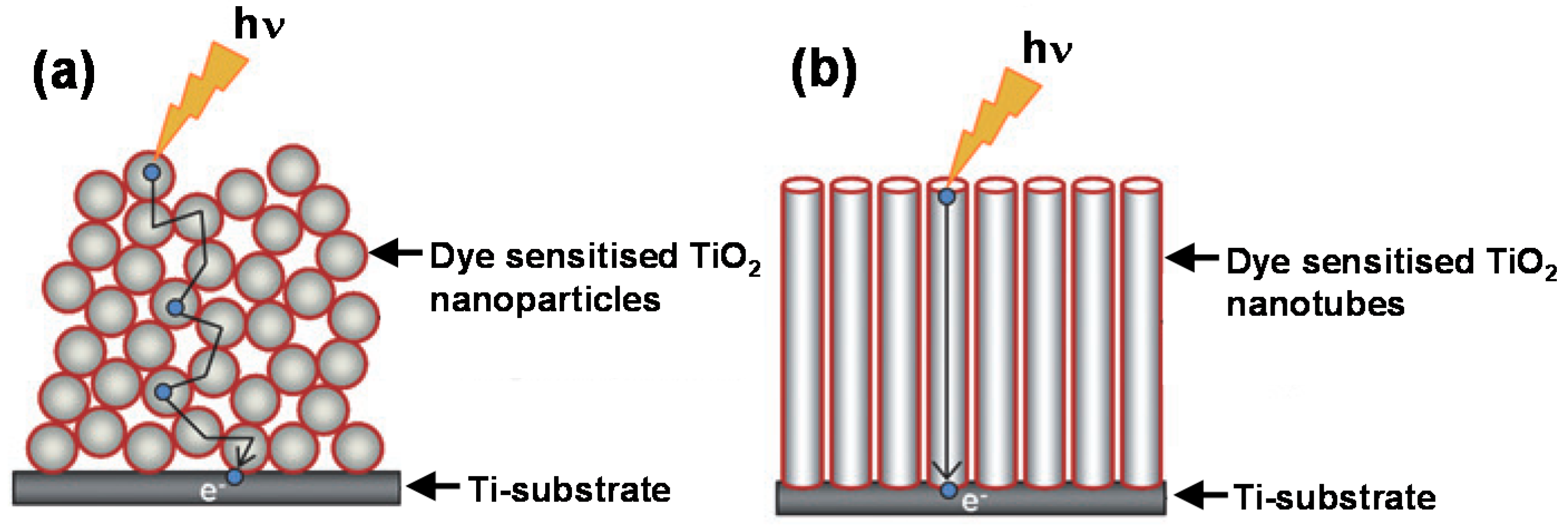
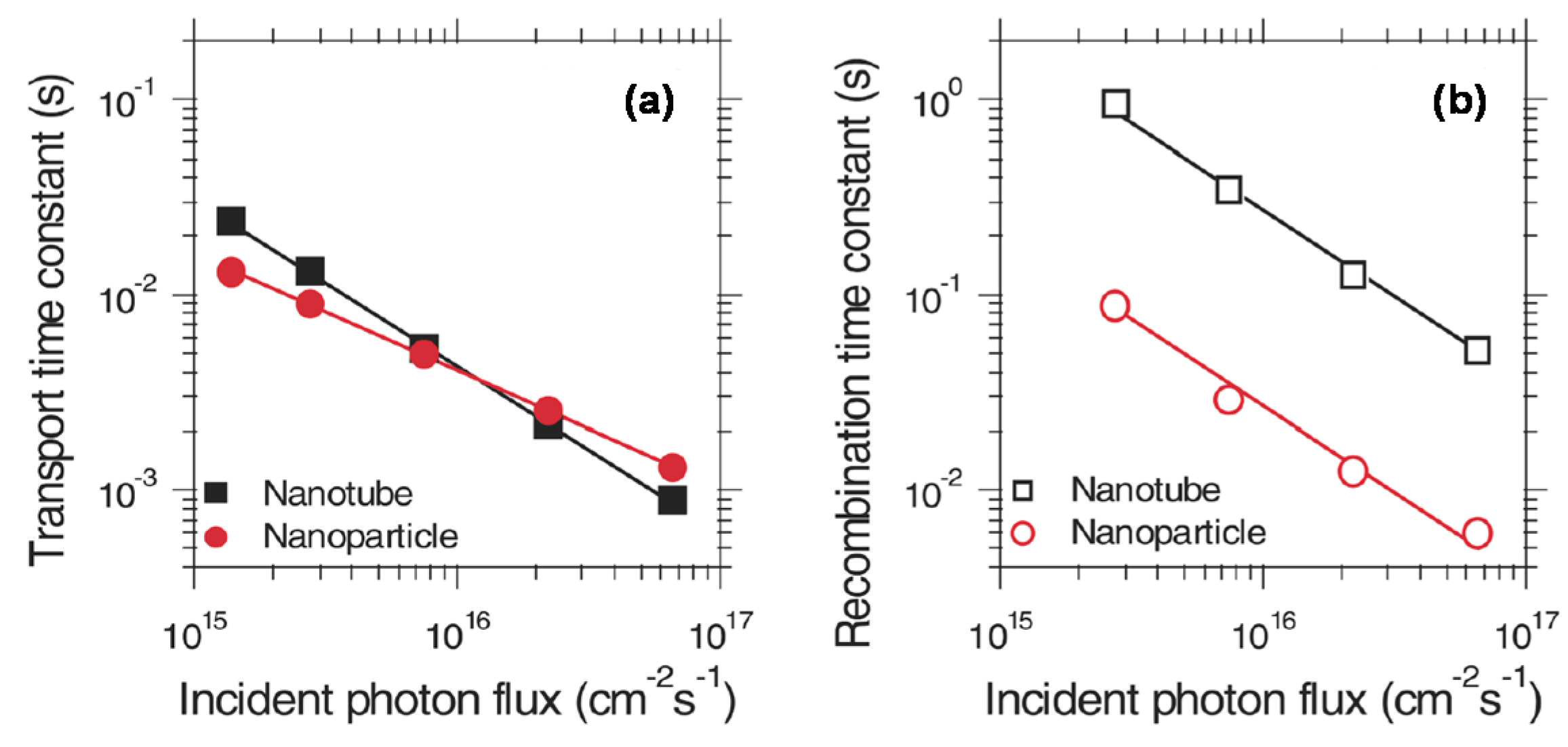
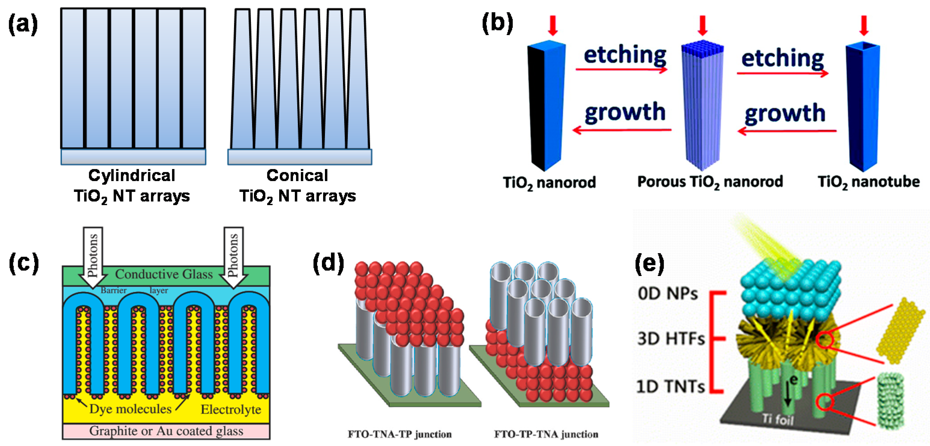
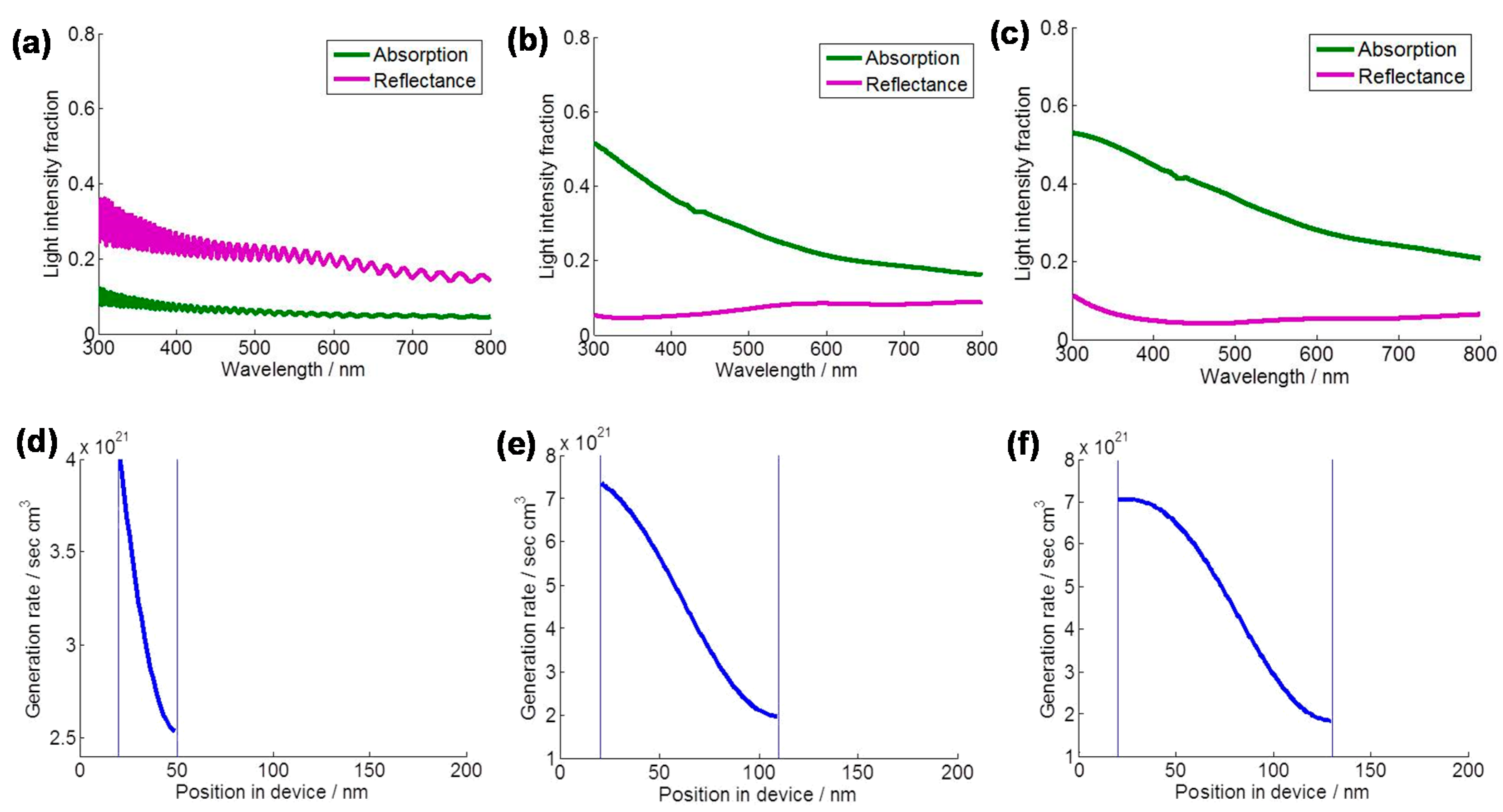
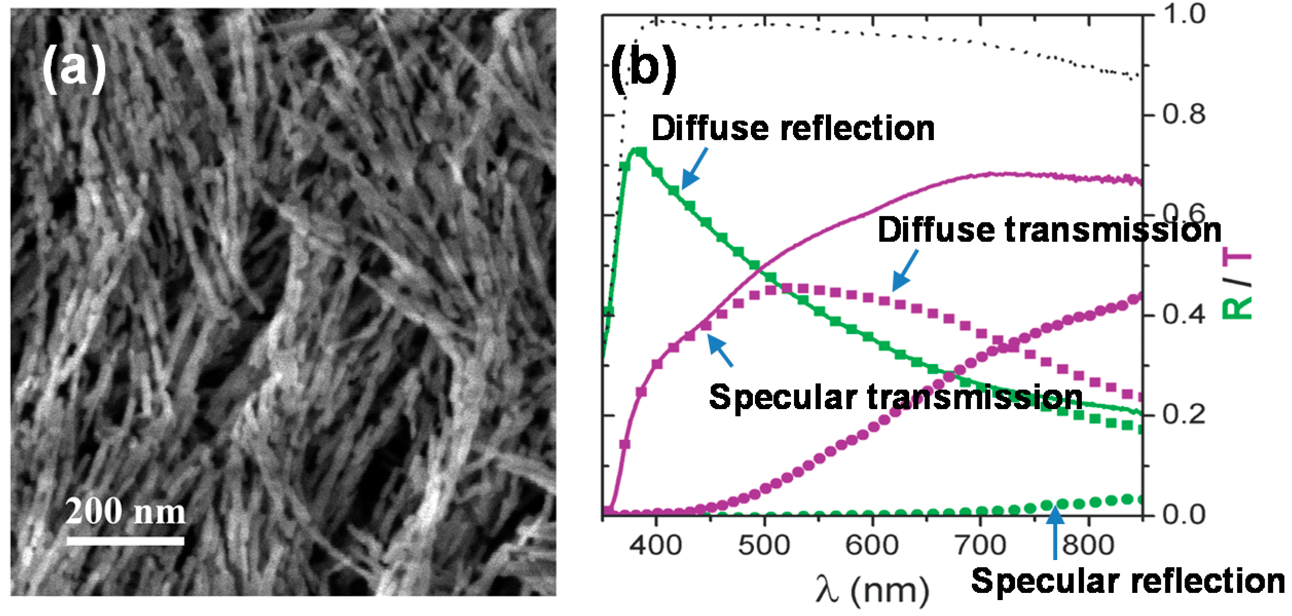
2. Novel Charge Transport and Optical Properties of 1D TiO2 Nanostructured Materials

In general, 1D nanostructures are prepared with a high aspect ratio, and at least one of the dimensions should be in the range of 1–100 nm. Based on the geometrical features, 1D nanostructures are typically of four different types: nanotubes (NTs), nanorods (NRs), nanowires (NWs), and nanobelts (NBs) [17]. NTs in particular possesses a hollow channel, whereas other three different types of nanostructures have a solid structure with no hollow channel. To clarify the differences between the NR, NW, and NB nanostructures, NR usually indicates a NW with a small aspect ratio, that is to say, a short NW [17,18]. NBs show a special NW structure with a rectangular cross-section, comprising single crystals with well-defined side crystal facets. Such geometrically unique 1D nanostructures offer novel material properties that differ from those of conventional nanoparticulate (NP) systems [17]. Obviously, the differences between 1D nanostructures and NP systems become apparent when they are applied to solar cell applications. Figure 1 shows schematic diagrams of the electron pathways in the randomly oriented mesoporous TiO2 NP- and well-oriented 1D TiO2 NT-based DSCs [19].
Mesoporous TiO2 NP layers have usually been regarded as the conventional photoanodes of DSCs due to their large surface area for effectively adsorbing dye sensitisers. However, mesoporous TiO2 NP layers in DSC structures are not ideal in the aspect of electron transport due to the following two reasons. (1) Electron drift, which is an essential electron transport mechanism in most photovoltaic cells, is prevented in DSCs by ions in the electrolyte that screen macroscopic electric fields and couple strongly with the moving electrons. (2) By the presence of numerous grain boundaries in TiO2 NP layers, electrons can easily be trapped, resulting in reduced electron lifetimes with the short electron diffusion length [20]. In the meantime, Zhu and co-workers [21] have reported a comprehensive investigation on charge collection efficiency in DSCs using vertically-oriented 1D TiO2 NT arrays. When comparing the charge transport time and recombination time of TiO2 NP- and TiO2 NT-based DSCs with a comparable thickness of TiO2 layers, both charge transport times were comparable, while the recombination time of TiO2 NT layers was 10 times slower than that of TiO2 NP layers, indicating the TiO2 NT-based DSCs have significantly (25%) higher charge collection efficiency than the TiO2 NP-based DSCs (Figure 2).
Likewise, TiO2 NR-based DSCs also showed longer electron lifetimes than TiO2 NP-based DSCs with a comparable electron diffusion coefficient where the lower lifetime of the NP layers might be due to the increased charge recombination rate caused by the presence of intraband gap states and electron loss between the grain boundaries [22]. Therefore, considering the higher charge collection efficiency with longer lifetime of 1D TiO2 nanostructures, the thickness of 1D TiO2 nanostructured layers in DSCs can become thicker than that of NP layers for a given recombination loss. In addition to the improvement of charge transport properties, light harvesting efficiency should also be considered for high efficiency solar cells. As seen in the following formula for a short-circuit current density (Jsc) of the photovoltaic performance, Jsc is determined by light harvesting efficiency as well as charge transport properties such as charge collection and injection efficiencies:
Jsc = q × ηlh × ηcc × ηinj × I0
where q is the elementary charge, ηlh is the light harvesting efficiency, ηcc is the charge collection efficiency, ηinj is the charge injection efficiency, and I0 is the incident photon flux (light intensity) [21]. Therefore, it is necessary to utilise a suitable light management strategy in enhancing the light harvesting efficiency, and one of these is the solar cell architecture. It is well-known that the optical properties of TiO2 nanostructures are closely related to their atomic arrangement and light injecting direction, so 1D TiO2 nanostructures with unique morphological properties can provide an excellent light scattering effect. A work by Nakayama and co-workers [23] compared TiO2 NP- and TiO2 NT-based DSCs with the same layer thickness of 10 μm, and their power conversion efficiencies were 5.27% with Jsc of 10.1 mA·cm−2 and 3.41% with Jsc of 7.4 mA·cm−2, respectively. Despite the lower amount of adsorbed dyes of the TiO2 NT-based, Jsc of the TiO2 NT-based was higher than that of the TiO2 NP-based, indicating a higher performance of the TiO2 NT-based that could be attributed to their higher light harvesting efficiency by the internal light scattering of TiO2 NT arrays. Meanwhile, Yun and co-workers [24] reported an investigation on optical modelling of DSCs with different thicknesses of TiO2 NT layers of 3.3 μm, 11.5 μm, and 20.6 μm via the generalised transfer matrix (GTMM) method. Based on the optical modelling, short 3.3 μm thick TiO2 NT-based DSCs presented relatively low light absorption with fluctuating light fraction intensity, while thicker TiO2 NTs with 11.5 μm and 20.6 μm showed significantly decreased reflectance results with the increased light absorption, followed by the higher charge generation rate with the increase in thickness of TiO2 NT (Figure 3) [24].
Besides vertically-oriented TiO2 NTs, even randomly-oriented TiO2 NWs led to intensive light scattering by the bundles of TiO2 NWs, thereby improving the optical absorption of the photoanodes (Figure 4). For a 2.5 μm thick TiO2 NW layers, 20% to 40% of visible light was observed to be scattered by transmission and refection [25].

3. Synthesis of 1D TiO2 Nanostructured Materials

1D TiO2 nanostructures can be prepared by a variety of synthetic methods, and depending on the method used, the morphological types and physicochemical properties of the 1D TiO2 nanostructures can be changed, thereby influencing the charge transport and optical properties in solar cell photoanodes. Another key point in synthesising 1D TiO2 nanostructures is the orientation status of 1D TiO2 nanostructured layers grown onto the substrates, which can be employed as the form of photoanodes. Thus, both randomly oriented and self-oriented cases of 1D TiO2 nanostructures are discussed with different synthetic methods.

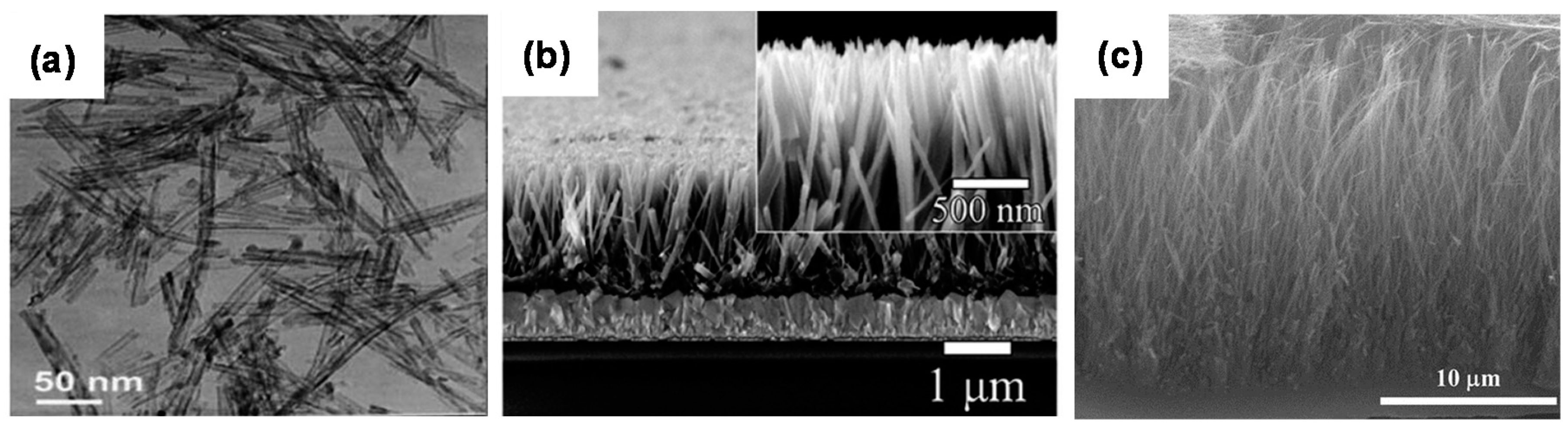
3.1. Hydrothermal Method

The hydrothermal method is a suitable synthetic approach to prepare single crystalline 1D TiO2 nanostructured materials which are dependent on the solubility of the precursors in water under high temperature and pressure conditions. Usually, the hydrothermal process is performed in an autoclave with a Teflon liner under controlled conditions of temperature, pressure, pH and additives. With such experimental conditions, different morphologies and crystal phases such as anatase, rutile and brookite can be obtained. As TiO2 nanoparticle-based suspension solution in alkaline condition are used as precursor for the hydrothermal reaction, suspended TiO2 nanoparticles are hydrothermally transformed into TiO2 NTs (Figure 5a) [26]. The formed TiO2 NTs can be selectively formed as anatase and rutile phases by using different precursor ratios, hydrothermal conditions, and salt incorporation [27,28]. Besides, it was reported that single crystalline anatase TiO2 NRs were transformed from NTs by the local shrinkage of the NT walls and the subsequent oriented attachment of crystallites when the pH of NT suspension in 10 M NaOH was controlled by dilute HCl solution in the ion-exchange process [29]. 1D TiO2 nanostructures can also be directly grown onto Ti metal substratse or conductive glass substrates through the hydrothermal process, and this would be beneficial to fabricate the 1D TiO2-based photoanodes for solar cells. Although the synthesis of the randomly oriented 1D TiO2 nanostructures can produce large amounts of 1D TiO2 materials with a large surface area, the randomly oriented 1D TiO2-based photoanodes should be prepared through the additional fabrication steps such as TiO2 paste preparation and doctor-blade printing. Therefore, in-situ growth of 1D TiO2 nanostructures onto the substrates would offer a simple and easy process and improved interfacial properties between 1D TiO2 layers and the surfaces of the substrates. Recently, many studies have reported the fabrication of vertically-oriented TiO2 NRs and NWs onto various substrates using hydrothermal methods as seen in Figure 5b,c. Without any substrates or seeding layers, the as-prepared 1D TiO2 materials were random and existed in a powder form, while vertically-oriented 1D TiO2 layers can be achieved in the presence of substrates with thin TiO2 seeding layers. The seeding layer could be prepared by dip- or spin-coating TiO2 precursor solution, followed by calcination of the layers at 450 °C for 1 h. Typically, titanium (IV) butoxide in HCl solution was applied as the precursor for the hydrothermal reaction, performed at 170 °C for 6 h. Then, the concentrated HCl constraint on the hydrolysis of the TiO2 precursor results in 1D TiO2 NRs. The growth of oriented 1D TiO2 NRs requires slow hydrolysis of the precursor in a strong acidic aqueous medium, while reduction in acidity of the precursor solution might have prompted hydrolysis of titanium (IV) butoxide. Through the optimised hydrothermal process with tuned hydrolysis condition, well-oriented single crystalline rutile TiO2 NRs with an excellent uniformity are obtained [30].

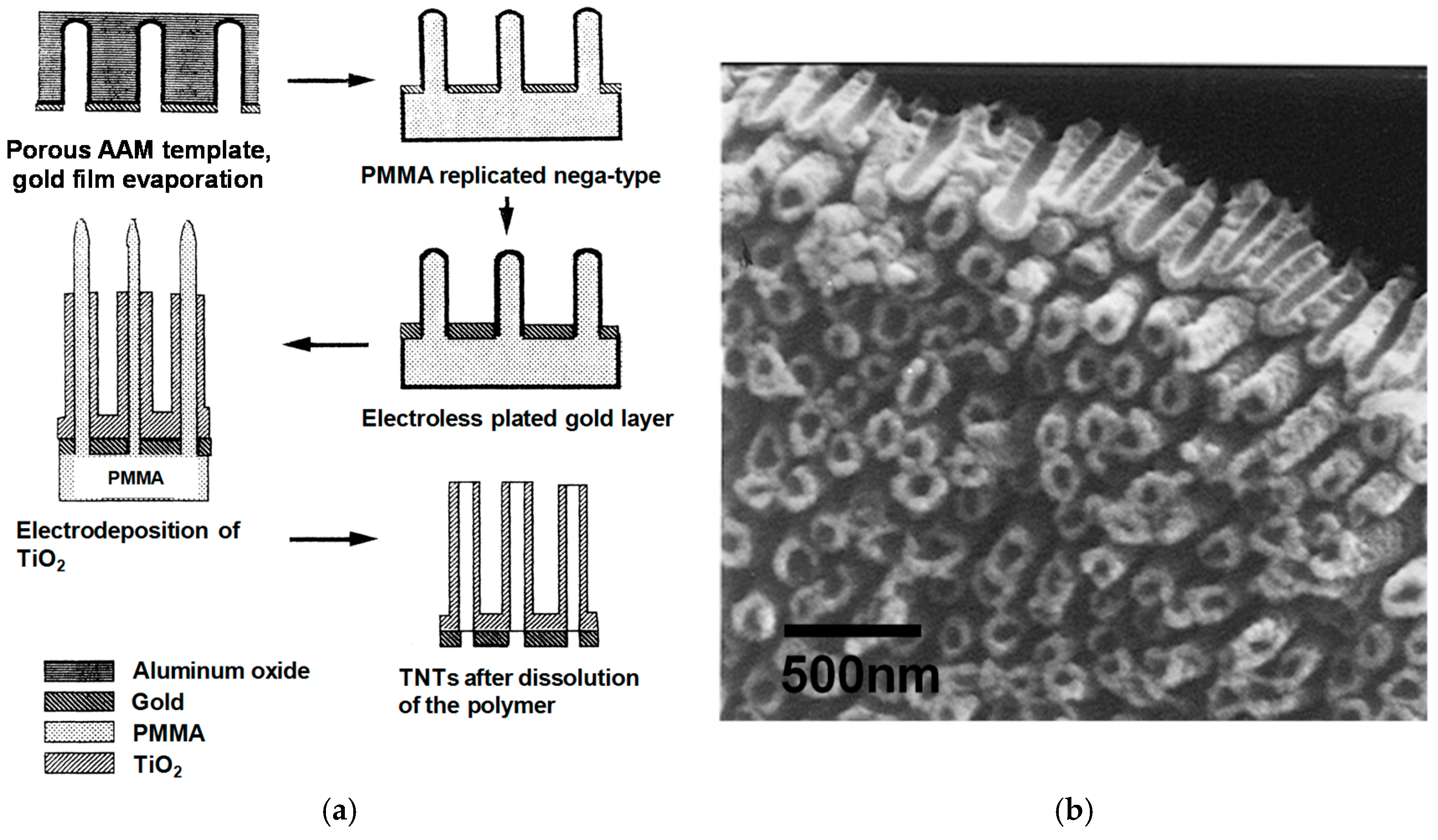
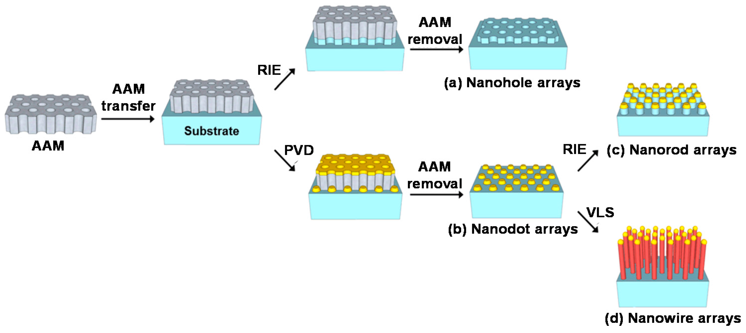
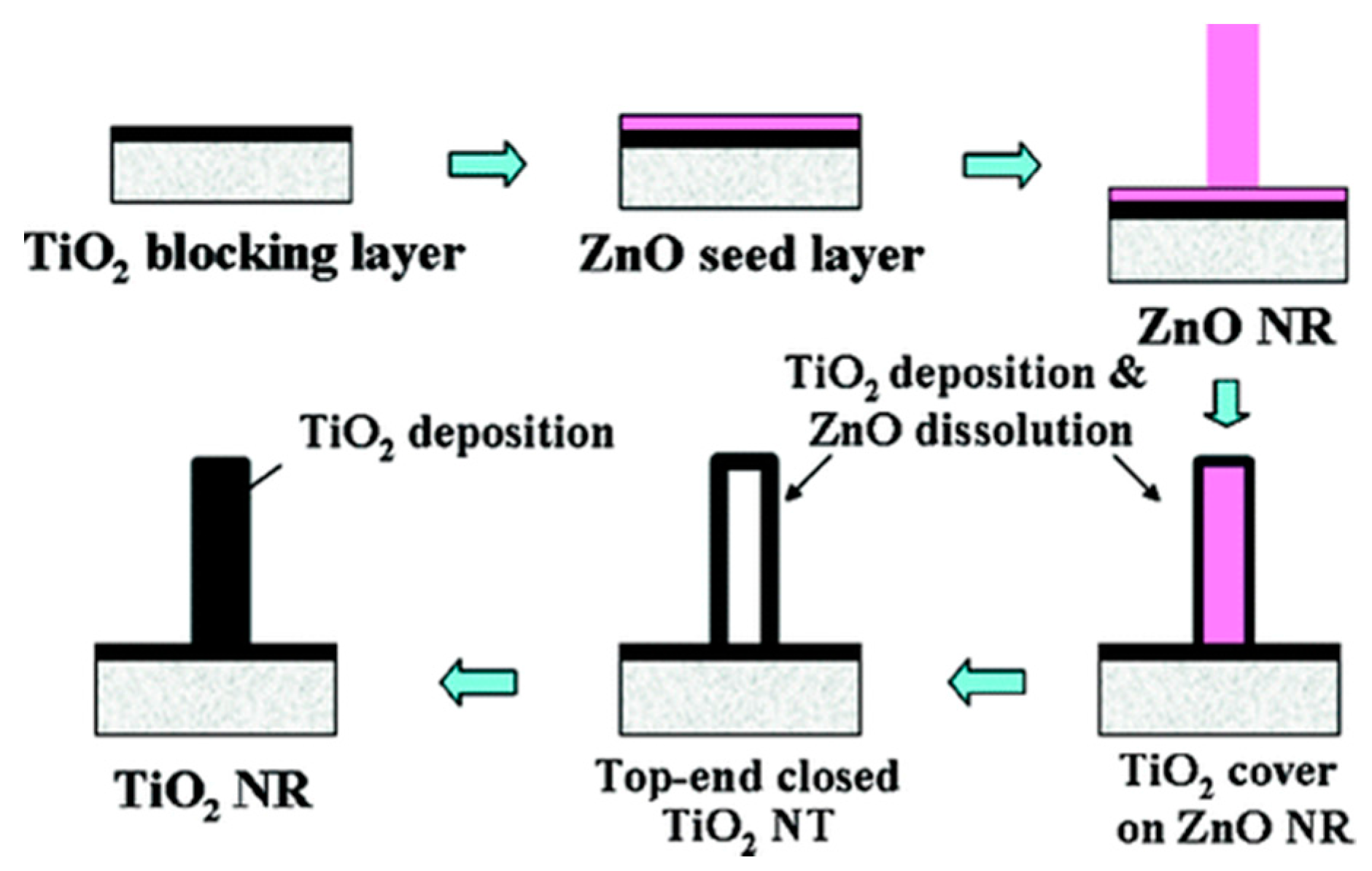
3.2. Template-Assisted Method

Template-assisted synthesis offers a reproducible synthetic approach for precise control over the size, shape and configuration, and growth direction of 1D nanostructured materials. In a typical template-assisted synthesis synthetic process, an anodised aluminium oxide membrane (AAM) is used as a template that possesses a self-oriented porous structure with tightly controlled pore size, density, and intervals. Thus, as Ti-precursors penetrate into the porous membrane structure through various deposition processes such as electrochemical deposition (ECD), atomic layer deposition (ALD), chemical vapour deposition (CVD), physical vapour deposition (PVD), sol-gel deposition, reactive ion etching (RIE), and vapor-liquid-solid (VLS) growth etc., well-oriented 1D TiO2 nanostructured materials with tunable dimensions such as lengths and diameter can be achieved. Figure 6 shows the general processes for the fabrication of well-oriented nanostructured arrays using an AAM template.
In Figure 6a,b, nanoholes and nanodots are a kind of intermediate stage prior to fabricating 1D nanostructures, and they can be prepared by RIE and PVD methods, respectively. In particular, nanodots can simply be achieved by depositing the precursors of the desired materials through an AAM template where the array pattern with controlled size and interdistance of the nanodots is defined by the template, and further well-oriented 1D nanostructured arrays are grown along the nanodot pattern.
Hoyer [34] first reported 1D TiO2 NT arrays using the template-assisted method via replication and electrodeposition process. Figure 7a shows fabrication of TiO2 NT arrays by electrodeposition of TiO2 onto the surfaces of polymethylmethacrylate (PMMA) rods as a template with gold film substrates replicated from porous AMM template. After dissolution of PMMA template in acetone at 40 °C, well-oriented TiO2 NT arrays were fabricated (Figure 7b).
Similar to the AAM template-assisted method, ZnO NR arrays can be employed as the template for 1D TiO2 NT arrays. Yodyingyong and co-workers [35] reported the formation of well-oriented nanoporous TiO2 NT arrays on transparent conductive oxide (TCO) substrates using ZnO NR arrays as the template. As seen in Figure 8, the ZnO NR template is prepared by the hydrothermal method, and then TiO2 NTs are formed onto the surfaces of ZnO NR template by immersing the template substrate in Ti-precursor solution at room temperature for 1.5 h, and further the ZnO templates are dissolved by TiO2 deposited ZnO template substrate in acidic solution for 1 h. More importantly, this ZnO NR template-assisted method offers in-situ assembly of well-oriented 1D TiO2 NT arrays with porous tube walls onto the TCO substrates. Although well-oriented 1D TiO2 nanostructures can be achieved through the AAM template-assisted method, adhesion issues near the interfaces between the 1D nanostructures and the surfaces of substrates occur. In particular, wet-etching the AAM template and transplanting 1D TiO2 arrays to the TCO substrates are necessary to fabricate the photoanodes for solar cells, but those processes may cause breakdown of unstable parts of 1D TiO2 nanostructures and poor interface properties due to adhesion issues, while ZnO NR templated onto TCO substrates may offer a proper solution due to the preferential etching characteristic along the (0001) orientation, facilitating the mild template removal with a top-down etching process. Additionally, the formation of porous walls of 1D TiO2 NT arrays by etching processes using TiCl4 contributes to a high surface area of 119 m2·g−1, expected to increase the amount of dye adsorption in DSCs.

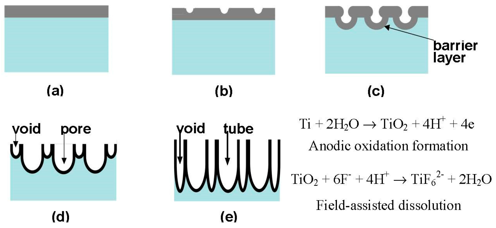
3.3. Electrochemical Anodisation Method

As discussed earlier, the template-assisted method seem to be more beneficial compared to the hydrothermal method in terms of reproducible preparation of well-oriented 1D TiO2 nanostructures with precise control of the geometric features such as lengths and diameters. However, the template-assisted methods require an additional dissolution process to remove undesired templates such as AAM, PMMA mold, and ZnO NR arrays. Furthermore, the dissolution process may also damage the desired 1D TiO2 nanostructures. Thus, the electrochemical anodisation approach for 1D TiO2 nanostructures has been of great interest in fabricating stable vertically-oriented TiO2 NT arrays because it is a template-free process with no additional post-treatment. The geometry of the anodised TiO2 NT array can readily be controlled by modulating the anodising conditions such as anodising time, electrolyte condition, and applied potential. In contrast, the template-assisted method is limited by the geometry of the applied template [14].
Typically, the anodic TiO2 NT arrays are grown by anodising pure Ti foil in an electrolyte including fluoride ions. During anodisation, the growth of TiO2 NT arrays is driven by the competition between anodic oxidation and chemical/field-assisted dissolution (equations in Figure 9). Figure 9 shows the comprehensive TiO2 NT growth mechanism by anodisation. When starting the anodization, dense and thin TiO2 layers are quickly formed onto the Ti foil substrates (Figure 9a), and subsequently undergo localised dissolution to form small pores (Figure 9b). The localised dissolution makes the barrier layer thinner, leading to an increasing electric field intensity across the barrier layer to further grow pores (Figure 9c). In fact, the barrier layer acts as a resistance to the flow of ions such as Ti4+ and O2−, which need to transport through the anodic oxide layer to maintain the oxidation active. In the meantime, higher resistance caused by thicker barrier layers can be overcome by increasing the applied potentials for a higher electric field. The presence of fluoride ions in the electrolyte allows the creation of channels in which current flows to keep the oxidation process active [36]. The thickness of the barrier layers underneath the pores/tubes is continuously reduced by dissolution, and simultaneously regenerated by oxidation. In Figure 9d, the electric field distribution at the bottom surface of the pore causes widening and deepening of pores. As the pores get deeper, the electric field in the exposed metallic regions increases, thus enhancing the field-assisted oxide growth and oxide dissolution. At the same time, the inter-pore voids start to be formed. Thereafter, both voids and pores grow in equilibrium. The TNT length increases until the oxidation rate at the metal/oxide interface equals the chemical dissolution rate of the top surface of the tubes (at the oxide/electrolyte interface). Afterwards, the TNT length is independent of anodizing time, as a result of a given electrolyte concentration and applied potential [37,38].
As the anodisation process is properly modified, defect-free anodic 1D TiO2 NT arrays can be fabricated. Wang and co-workers [39] demonstrated a novel protocol to prepare defect-free 1D TiO2 NT arrays using a two-step anodisation process. In the first anodisation step, the grown NT arrays are peeled off thereby the ordered footprint of NTs are left on the surface of the Ti substrate. After the second anodisation step, nanoporous-layer-covered well-aligned NT arrays are obtained. The defect-free condition of 1D TiO2 nanostructures as the photoanodes for solar cells would suppress charge recombination by reducing charge trapping sites.
The morphology of well-oriented TiO2 NT arrays can be tuned by modulating anodising conditions, thereby length, pore diameter, and wall thickness, and wall surface roughness are controllable. Yun and co-workers [14,40,41,42] comprehensively investigated the geometrical properties of TiO2 NT arrays with different experimental conditions. Under the optimised anodisation conditions with the applied potential of 60 V in the electrolyte containing 0.5 wt % NaF and 5 wt % water, geometry of TiO2 NT arrays was significantly changed with anodising time. As seen in Figure 10a,b, 3 h-, 10 h-, and 15 h-anodised TiO2 NT arrays present 3.3 μm, 11.5 μm, and 20.6 μm in length, respectively, and the pore diameter also increases from 50 nm to ~90 nm with the increase in anodising time.
The proportional increase in NT lengths can be attributed to the continuous oxidation of Ti foil, whereas the decrease in tube wall thickness is due to chemical dissolution of the oxide. In Figure 10c, well-oriented TiO2 NT arrays are observed over the large area of Ti foil substrates with the uniform growth of lengths and pore diameters, and those TiO2 NT arrays can directly be employed as the photoanodes of solar cells without further fabrication processes [14,24].

4. 1D TiO2 Nanostructure-Based Solar Cell Applications: DSCs and PSCs

In light absorber-sensitised solar cell systems such as DSCs and PSCs, the photovoltaic performance is driven by the charge transport properties and light harvesting efficiency, and therefore strategic approaches to enhance electron transport and lifetime and light scattering should be considered. In this regard, 1D TiO2 nanostructured materials would be an excellent candidate to meet such requirements in the cases of both DSCs and PSCs owing to the novel charge transport and optical features of unique 1D TiO2 nanostructures. In this review, thus, as 1D TiO2 nanostructures are applied as the photoanodes, the desirable strategical architectures in DSCs and PSCs will be discussed with various ideas suggested by the current research progress.

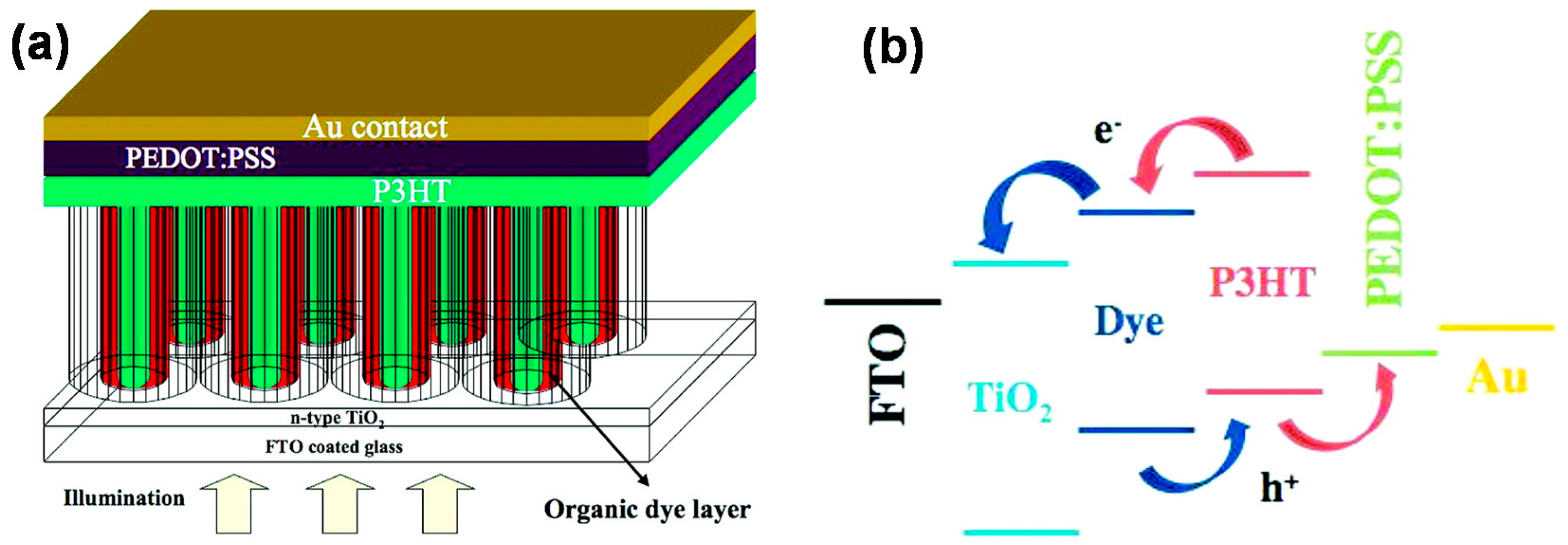
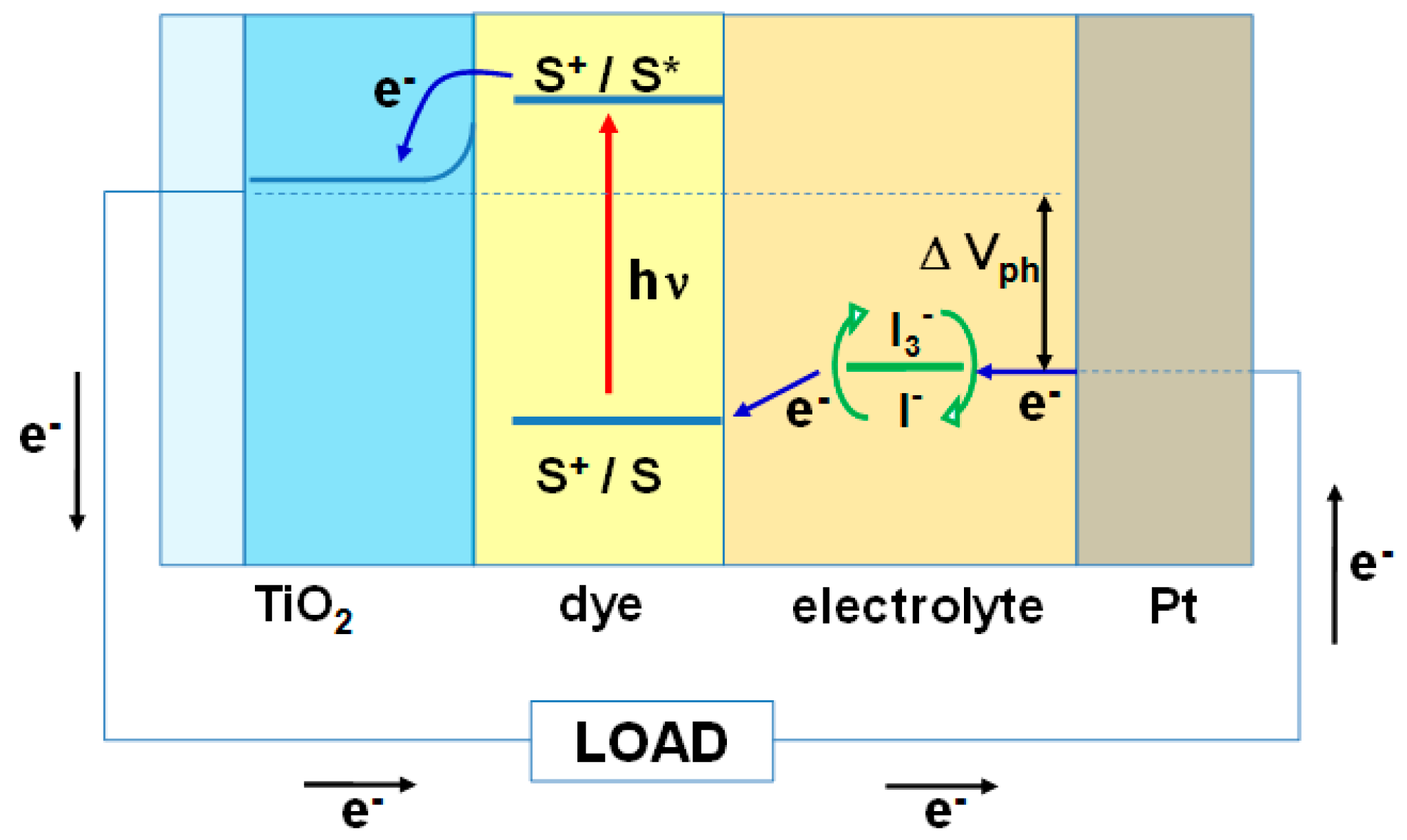
4.1. 1D TiO2 Nanostructure-Based DSCs

In 1991, O’Regan and Gratzel [3] reported low-cost DSCs fabricated using mesoporous TiO2 layers. The DSCs are basically a thin-layer solar cell fabricated by sandwiching two TCO electrodes (typically fluorine-doped tin oxide or indium-doped tin oxide). The photoanoode is composed of a mesoporous TiO2 layer adsorbed with a dye as a photosensitiser deposited onto the TCO substrate. The counter electrode is composed of finely distributed Pt films deposited on another TCO substrate. The inner space between a photoanode and a counter electrode is filled with a liquid electrolyte containing I/I3 redox couple in acetonitrile. Figure 11 presents a schematic diagram on the principles of DSC operation. Under sunlight illumination, excited electrons generated from the dyes are injected into the conduction band of TiO2, and then the injected electrons diffuse to the TiO2/TCO interfaces through the mesoporous particulate network, where electrons are extracted to the external load.
Meanwhile, the resulting oxidised dyes are reduced rapidly to the ground state by I in the electrolyte and the electrons reaching the Pt counter electrode through the external load reduce back the formed I3 to I, thereby the DSCs have a cyclic electron transfer process [3,43,44]. The current best PCE obtained from the DSCs is 12.3% using porphyrin sensitisers and cobalt (II/III) redox electrolyte [45]. In the development of 1D TiO2 nanostructure-applied DSCs, 1D TiO2 NTs prepared by a hydrothermal method were first applied to DSCs. Compared to mesoporous TiO2 NP systems using commercial P25 TiO2 nanoparticles, TiO2 NT-DSCs showed higher PCE of 6.4% than TiO2 NP-DSCs with PCE of 5.5%, attributed to the improved electron transfer along the NT structure. After TiCl4 post-treatment, the PCE of 1D NT-applied DSCs further increased to 7.1%, which is attributed to the facilitation of the electron transport by the improved interparticle connectivity [46]. Karthik and co-workers [47] reported backside-illuminated DSCs with vertically oriented TiO2 NT arrays with long lengths of 20 μm, achieving a PCE of 6.9%. However, 1D TiO2-DSCs have still been struggling to reach the high photovoltaic performance of the mesoporous TiO2-based DSCs. The lower efficiency of 1D TiO2-DSCs is mainly due to the relatively low light harvesting efficiency that can be attributed to the small amount of dye adsorption by their small surface area and low transmittance by backside-illumination. Recently, various strategies to overcome those drawbacks by surface engineering and electrode architecture have been reported. So and co-workers [48] achieved high PCE of 8.09% with conical-shaped TiO2 NT arrays as the photoanodes under backside-illumination conditions, wherein the conical-shaped TiO2 NT arrays were prepared by two step anodisation processes using an electrolyte containing 0.2 M NH4F, 50 vol.% lactic acid and 50 vol.% triethyleneglycol (Figure 12a). In spite of light absorption loss by the backside-illumination, the significant improvement of 1D TiO2 NT-DSCs was mainly due to the efficient light utilisation management by the conical shaped tips of the tubes. Although the modification of the 1D nanostructures can contribute to improving the light utilisation in solar cells, the backside-illumination condition still limits the overall light harvesting efficiency so that the frontside-illumination condition is more preferable to enhance the overall photovoltaic performances of the cells. As shown in Figure 12b, Lv and co-workers [49] applied porous rutile TiO2 NR arrays onto TCO substrates for enhancing the performance of DSCs, where ~30 μm thick TiO2 NR arrays were prepared by a hydrothermal method, and the completed NR arrays were further etched by HCl. The etched TiO2 NR arrays showed much higher dye loading compared to their counterpart mesoporous TiO2, leading to an improved PCE of 7.91% with Jsc of 20.49 mA·cm−2. Figure 12c shows the anodised 1D TiO2 NT arrays are directly grown onto the TCO substrates. In this case, instead of Ti foil substrates, Ti metal deposited TCO was used as the source material for the anodisation, and thus TiO2 NT arrays can be strongly grown onto the TCO substrates [50]. Hierarchical designs integrating more than two heterostructured nanomaterials provide multiple advantages in optimising the solar cell architectures. As seen in Figure 12d,e, 0D and 3D nanostructured materials can be incorporated with 1D nanostructured materials in various arrangements, leading to efficient light scattering and electron transport properties and large dye loading, followed by improving overall photovoltaic performances. Similar to Figure 12c, Figure 12d also presents frontside-illuminated 1D TiO2 NT-DSCs using the anodised TiO2 NT arrays. However, in this work, the fabrication procedure of the anodised 1D TiO2 NT arrays onto the TCO substrates is different from that of Figure 12b. Instead of using Ti metal deposited TCO substrates, the anodised TiO2 NT arrays were transplanted onto the TCO substrates by imprinting the peeled off the TiO2 NT arrays from Ti foil substrates. When applying the peeled off TiO2 NT arrays as the photoanodes, randomly oriented TiO2 NPs are incorporated onto the bottom or the top of the TiO2 NT arrays. In the junction structure of “FTO-double TiO2 NP layers-17 μm thick TiO2 NT arrays”, the photoelectron lifetime was extended by 237.5% and the PCE was 8.8% with Jsc of 18.89 mA·cm−2 [51]. In Figure 12e, the photoanodes are composed of branched 0D-3D TiO2 composites on TiO2 NT arrays at the bottom, where 0D TiO2 nanoparticles are on the top of the 3D TiO2 microspheres. Particularly, the branched 1D TiO2 NT arrays and 0D-3D TiO2 nanocomposite layers provide rough surfaces, contributing to improving the charge transport capacity and light harvesting efficiency, resulting in a PCE of 9.1% with Jsc of 17.9 mA·cm−2 [52].
Taking all the above 1D TiO2 photoanode designs for DSCs into account, the use of 1D TiO2 nanostructures as the photoanode in solar cells leads to a significant change in designing solar cell device structures compared to the conventional mesoporous TiO2 photanode systems with randomly oriented structures, wherein both advantages and disadvantages of 1D TiO2 nanostructures in solar cell application can be found. Although the relatively smaller surface area of 1D TiO2 nanostructures results in low device performance due to the low dye loading amount, such drawbacks can be overcome through strategic approaches to modify 1D TiO2 nanostructures and the architecture of 1D TiO2-DSCs. Specifically, the low light harvesting efficiency of 1D TiO2-DSCs is a key issue in improving device performance, and it can be improved by excellent light scattering effect of the modified conical shaped TiO2 NTs (Figure 12a) and increasing incident light absorption by the front illumination device architecture (Figure 12c). Another approach to enhance light harvest efficiency is by increasing the surface areas of 1D TiO2 photoanodes to uptake a large amount of dyes. This can be achieved by using porous 1D TiO2 nanostructures (Figure 12b) and 0D/3D/1D integrated TiO2 nanostructures (Figure 12d,e). In particular, the integrated 1D TiO2 photoanodes lead to significantly improved light harvesting efficiency through the synergistic effect of the integrated 0D/3D nanoparticles with large amount of dye loading and enhancing light scattering. Recently, Mahmood and co-workers [54] have reported highly efficient hyperbranched 3D TiO2 photoanodes consisting of four-layered 1D TiO2 nanostructured arrays with a PCE of 11.22%, which is comparable to that of high efficiency DSCs using mesoporous TiO2 photoanodes. The remarkable performance of the unique hyperbranched structured DSCs is due to their significantly enhanced electron lifetime and light harvesting efficiency, demonstrating the great potential of the hyperbranched structures in next generation solar cells.
As the intermediate stage in DSC progress prior to PSCs, solid-state DSCs (SSDSCs) have been extensively studied as the alternative way to solve some of the potential drawbacks of DSCs. Although DSCs have already achieved a high PCE of 12.3%, the liquid electrolyte in DSCs may cause potential leakage and corrosion problems. Thus it would be meaningful to replace liquid electrolytes with solid electrolytes to overcome such disadvantages of DSCs. In addition, 1D TiO2-SSDSCs have also been investigated as one of the promising approaches for high performance. Most importantly, it is noted that the working mechanism and the device structure of SSDSCs are analogous to those of PSCs. Thus, it would be meaningful to briefly review 1D TiO2-SSDSCs before moving on to the 1D TiO2-PSC applications. The main key in SSDSCs would be the use of solid-state hole transport materials (HTMs) to replace the liquid electrolytes found in DSCs. Typically, p-type inorganic materials or organic materials are applied as the HTMs in SSDSCs. spiro-MeOTAD (2,2′,7,7′-tetrakis-(N,N-di-p-methoxyphenylamine)-9,9′-spirobifulerene) is used as HTM in SSDSCs [55]. The SSDSCs using spiro-MeOTAD as a HTM have already achieved a PCE of 5.1%, but this PCE is still lower than that of DSCs using liquid electrolytes [56]. Ding and co-workers [57] recognised that the main reason would be a pore filling issue of HTM into the dye-sensitised photoanode internal structure, and it was indicated that a 2.5 μm thick TiO2 layer with 60%–65% pore filling prepared by optimising the spin coating conditions was the best solution. Likewise, in the case of 1D TiO2-SSDSCs, the optimised pore filling conditions should be investigated by considering the thickness of 1D TiO2 arrays and spin coating conditions. Mor and co-workers [58] investigated 1D TiO2 NT-SSDSCs, mimicking a typical bi-layered organic photovoltaic architecture as seen in Figure 13a. In this device structure, 1D TiO2 NT arrays were fabricated by anodising Ti metal-deposited TCO substrates (refer to Figure 12b), and poly(3-hexylthiophene-2,5-diyl) (P3HT) as a p-type HTM and PEDOT:PSS as an electron blocking layer were applied to SSDSCs. In the charge transfer processes of Figure 13b, excited electrons from dye and P3HT are injected to the conduction band of TiO2, while holes are efficiently separated and transferred to Au through the PEDO:PSS layers by a p-type P3HT HTM.
As pore filling is a key issue in SSDSCs, the deposition of P3HT into the NTs was performed by spin coating after pre-wetting NT arrays with p-xylene, a non-polar solvent, acting to penetrate P3HT inside the NT arrays. With 600–700 nm thick and ~35 nm pore diameter, the achieved PCE was 3.8%. Roh and co-workers [59] reported high efficiency SSDSCs prepared using hierarchical anatase pine tree-like TiO2 NT (PTT) arrays in which the hierarchical anatase PTT arrays were fabricated directly onto the TCO substrates by a one-step hydrothermal method. The applied electrolyte was poly((1-(4-ethenylphenyl)methyl)-3-butylimidazolium iodide) (PEBII), which was deposited onto the PTT arrays by two-step drop casting. The SSDSCS assembled with 19 μm thick PTT arrays showed an excellent PCE of 8%, which was twice higher than that of commercially available TiO2 paste with a PCE of 4%, representing one of the highest records achieved from N719 dye-based SSDSCs. In Table 1, we summarise the photovoltaic performance of DSCs and SSDSCs using 1D TiO2 nanostructured photoanodes.

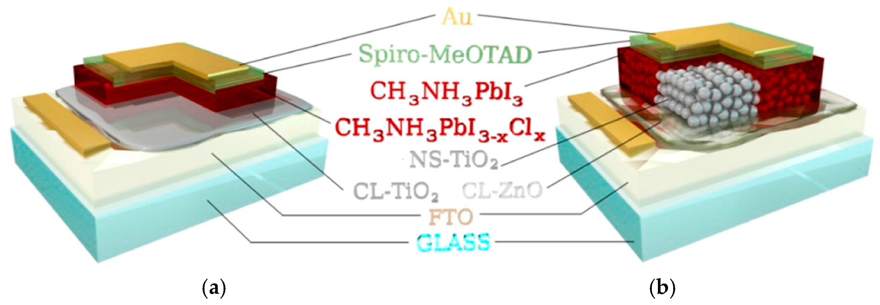
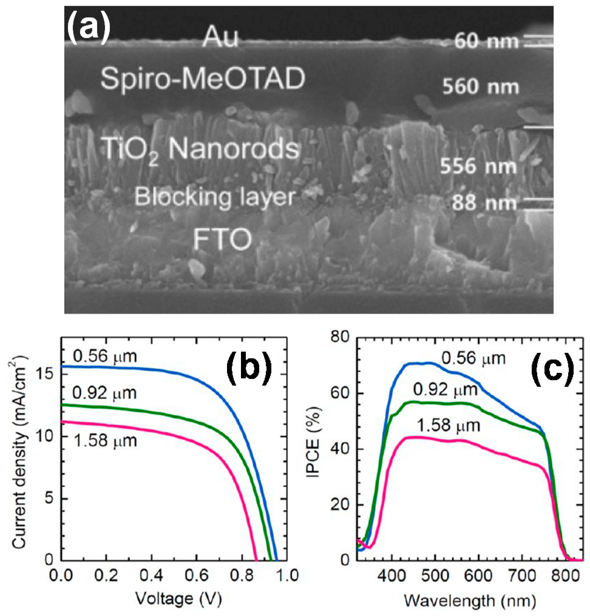
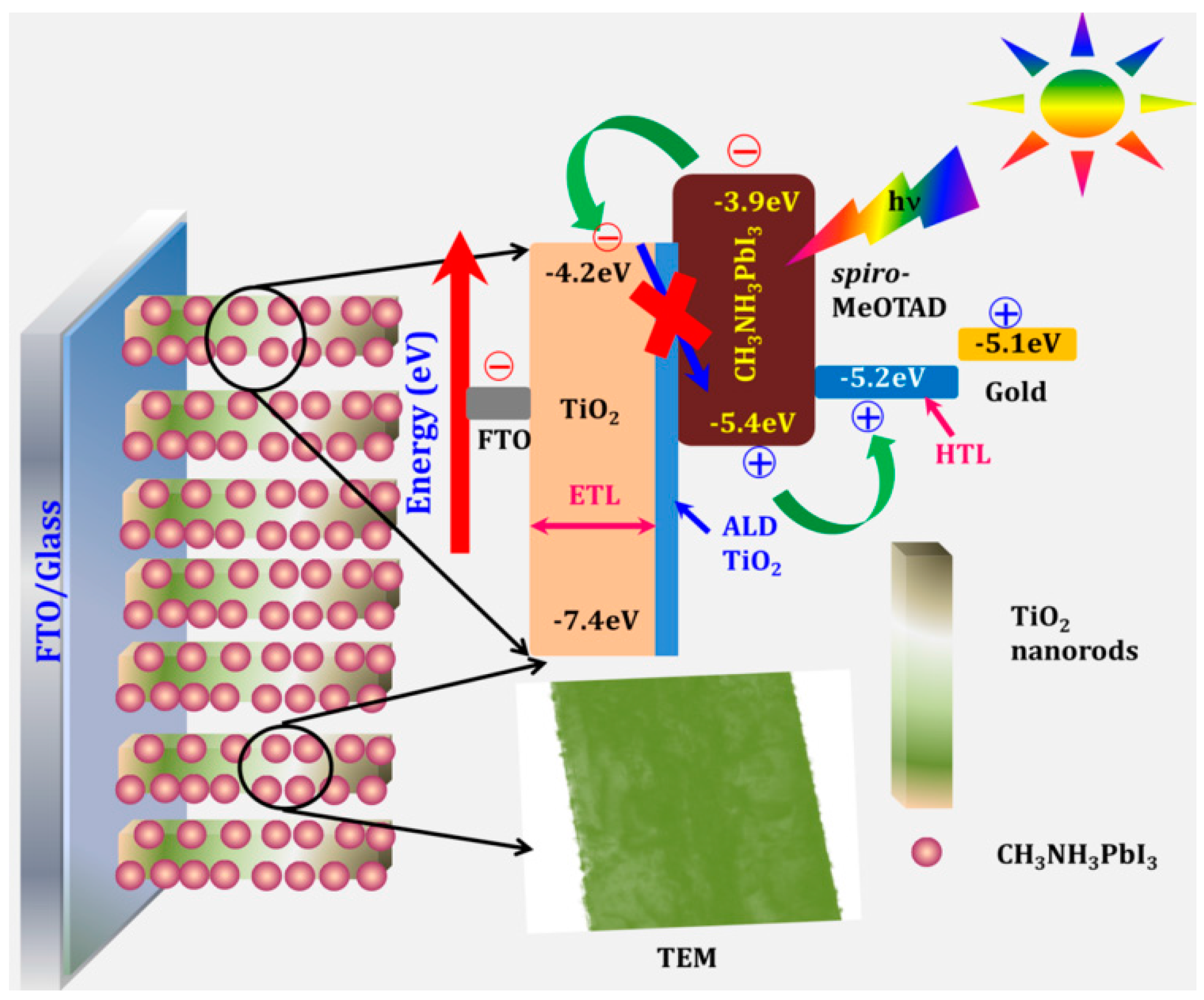
4.2. 1D TiO2 Nanostructure-Based PSCs

Since Kojima and co-workers [4] first reported PSCs comprising perovskite light absorbers such as CH3NH3PbI3 and CH3NH3PbBr3 in a liquid electrolyte, the progress of PSCs has been dramatically fast in a short-term period. Recently, Seok’s group [5,64] has reported a world-best PCE record of 22.1% achieved by incorporating methylammonium (MA) and formamidinium (FA) ions, which has attracted great attention to the potential of low-cost and simple solution processed solar cells compared to expensive Si-based solar cells. The working mechanism of PSCs is shown in Figure 13. Basically, PSCs are composed of an n-type perovskite-sensitised photoanode, p-type HTM layer, and an Au metal contact. Depending on the presence of TiO2 active layers, PSCs can be classified to two different device structures: Figure 14a indicates planar structured PSCs without a TiO2 active layer, while Figure 14b presents mesoscopic PSCs with a mesoporous TiO2 active layer. Similar to the working principles of DSCs and SSDSCs, electron-hole charge separation by injecting electrons from perovskites to TiO2 take place in PSCs, and subsequently the injected electrons are extracted to an external load through the TCO (FTO) substrate, while the separated holes from the perovskite are transferred to Au metal contact via a HTM layer. However, due to unique perovskite properties such as charge transport and charge accumulation, the working mechanism should be different from DSCs and SSDSCs.
For instance, CH3NH3PbI3−xClx perovskite thin films shows both electron and hole diffusion lengths are over 1 μm, indicating a dimension 5–10 times greater than the absorption depth. The larger diffusion length leads to a much longer recombination lifetime [66]. Electron and hole mobilities were also found to be as high as 25 cm2·Vs−1, and both mobilities were almost balanced and remained high along with a slow microsecond time scale for recombination [67]. However, the photovoltaic performance may decrease in case the mobility of the injected electrons in the TiO2 layer is slower than that of the perovskites. Thus, as considering the diffusion length and the mobility of the injected electrons, strategical design of the TiO2 layers would be important to improve the performance [6]. Since the advantages of 1D TiO2 nanostructures in DSCs are still a promising option in designing the device structure of PSCs, the use of 1D TiO2 nanostructures would contribute to improving the performance of PSCs. In comparison with the absorption coefficient of Ru-based N719 dye, the absorption coefficient of CH3NH3PbI3 perovskite was an order of magnitude higher than that of the N719 dye. Furthermore, despite the small amount of perovskite loading onto TiO2, the photocurrent density was twice higher than that of the fully loaded N719 dye onto TiO2 [68]. In this regard, Kim and co-workers [69] first employed TiO2 NR arrays as the photoanode to PSCs using CH3NH3PbI3 perovskite (Figure 15a). In Figure 15c, the PCE was the highest at 9.4% with 560 nm thick NR arrays, and the performance decreased with an increase in NR lengths. This indicates that the shorter NRs more efficiently utilise the short wavelength light than the longer NRs, related with the higher pore filling fraction of the short NRs.
Wu and co-workers [70] investigated the dimensional effects of TiO2 electron transport layers (ETL) in the PSC performance by comparing 0D NP, 1D NW, and 2D nanosheets (NS), where TiO2 NP, NW, and NS were tuned by the different organic solvents during the solvothermal reaction. These fabricated TiO2 layers presented enhanced optical transparency, minimising light absorption loss. The photovoltaic performances of PSCs using 1D NW and 2D NS photoanodes were higher than that of the 0D NP counterparts. Basically, efficient infiltration of perovskite sensitisers in 1D NW and 2D NS structures would improve light absorption efficiency. Particularly, 1D NW-based PSCs demonstrated an excellent performance with a PCE exceeding 16%, which was due to the bilayered ETL system consisting of a self-assembled compact and thin TiO2 blocking layer and NW active layer. This bilayered ETL film can lead to blocking the photogenerated holes and improve electron extraction, thereby enhancing PSC performance.
Similar to the DSCs, 3D/1D combined layered hyperbranched TiO2 NR photoanodes also led to improving PSC performance, indicating a PCE of 15.5% with Jsc of 20.5 mA·cm−2, Voc of 1 V, and FF of 0.75. 3D hyperbranched structures are suitable for high light harvesting efficiency with large surface area, while 1D NRs included in the 3D hyperbranched structures can efficiently transfer electrons over long distances, suppressing recombination losses.
Surface engineering of 1D TiO2 NRs by the atomic layered deposition (ALD) method provides a uniform and ultrathin passivation layer on the surface of NRs, leading to improved photovoltaic performance with high Voc and FF. The enhancement of Voc and FF is mainly due to the interface properties. The ultrathin passivation layer by ALD offers pinhole-free surfaces over the TCO substrates and TiO2 NR arrays, thereby improving pore filling and charge generation, and reducing recombination. Particularly, the back-flow of electrons from the TiO2 conduction band to CH3NH3PbI3 and HTM was minimised by the ALD passivation layer (Figure 16). With the optimised ALD passivation thickness of 4.8 nm, the PCE of 1D TiO2 NR-PSCs was 13.45% with Voc of 0.945 V, Jsc of 19.78 mA·cm−2, and FF of 72% [54].
Recently, Lin and co-workers [72] have reported the best efficiency of 1D TiO2 NR-PSCs by optimising NR diameter, densities, and surfaces through a facile solvothermal method. Surface treatment using UV-ozone on TiO2 NR array also contributed to increasing the PCE from 13.58% to 14.72%. Through the surface treatment, the remaining organic contaminants resulting from the solvothermal process could be successfully removed, and further the adhesion between NR array and the perovskite layer was strengthened by the surface modification, which could promote faster electron injection between the perovskite layer and TiO2. Therefore, an enhancement of Jsc, Voc, and particularly FF was obtained from the PSCs with surface-treated TiO2 NR arrays, leading to a higher PCE. With the optimised perovskite capping layer atop the TiO2 NR array, an encouraging PCE of 18.22% has been achieved with Jsc of 22.9 mA·cm−2, which is the highest efficiency reported so far for 1D nanostructure-applied PSCs. Most importantly, the high performance and simple surface modification method of the TiO2 NR-PSCs are encouraging to compete with the conventional mesoscopic PSCs with mesoporous TiO2 photoanode [72]. Table 2 summarises the photovoltaic performance of the 1D TiO2 nanostructured photoanode-employed PSCs.

5. Conclusions

In this review article, the novel properties, synthetic methods, and applications of 1D TiO2 nanostructures have been reviewed, with a focus on photoanodes for solar cell applications. Basically, the photovoltaic performance of solar cells is driven by the charge transport properties and light harvesting efficiency, which can be improved by optimising the photoanode materials and device architecture. Thus, it is important to note that the unique morphology of 1D TiO2 nanostructures offers excellent charge transport properties such as charge separation, electron injection, and electron lifetime. Besides, 1D TiO2 nanostructures lead to efficient light utilisation management by light scattering and channeling effects. In comparison to randomly oriented TiO2 nanoparticulate systems, the vertically oriented 1D TiO2 NTs and NWs present significantly improved charge transport properties and light harvesting efficiency in DSCs, followed by the improvement of overall photovoltaic performance of the devices. In particular, the hierarchical architecture incorporating 0D TiO2 nanoparticles or 3D hollow TiO2 microspheres to 1D TiO2 nanostructures can further improve the performance with their large surface area as well as 1D structured light scattering layer and express electron channels. In PSCs, 1D TiO2 nanostructures can also be a promising candidate for high efficiency solar cells. Especially, the much higher light absorption coefficient and extremely long charge diffusion lengths of the perovskites would be beneficial to remedy a drawback of 1D TiO2 nanostructures, their relatively low light harvesting efficiency caused by the lower dye loading in DSCs. However, the 1D TiO2-PSCs have not been extensively studied yet, compared to the case of 1D TiO2-DSCs, indicating there is still much room to further develop 1D TiO2-PSCs. Since the key issues of 1D TiO2-PSCs are pore filling and optimising the device architecture using 1D TiO2 nanostructured layers, various deposition methods, newly developed perovskites and HTMs, and advanced PSC architectures should be preferentially considered to achieve high performance of 1D TiO2-PSCs. In addition, studies of 1D TiO2-applied flexible and large scale devices may provide insights into the commercialisation of DSCs and PSCs in the near future.

Acknowledgments

The authors would like to acknowledge financial support from Australian Research Council through its DP (DP110101638) and FF programs. This work was performed in part at the Queensland node of the Australian National Fabrication Facilities.

Author Contributions

Jung-Ho Yun and Yun Hau Ng conceived and designed the structure of this work; Rose Amal and Lianzhou Wang contributed discussion on all the sections; Jung-Ho Yun wrote the paper.

Conflicts of Interest

The authors declare no conflict of interest.

References

  1. Lewis, N.S.; Crabtree, G. Basic Research Needs for Solar Energy Utilization: Report of the Basic Energy Sciences Workshop on Solar Energy Utilization; US Department of Energy, Office of Basic Energy Science: Washington, DC, USA, 2005.
  2. Matsumura, M.; Matsudaira, S.; Tsubomura, H.; Takata, M.; Yanagida, H. Dye sensitization and surface structures of semiconductor electrodes. Ind. Eng. Chem. Prod. Res. Dev. 1980, 19, 415–421. [Google Scholar] [CrossRef]
  3. O’Regan, B.; Gratzel, M. A low-cost, high-efficiency solar cell based on dye-sensitized colloidal TiO2 films. Nature 1991, 353, 737–740. [Google Scholar] [CrossRef]
  4. Kojima, A.; Teshima, K.; Shirai, Y.; Miyasaka, T. Organometal halide perovskites as visible-light sensitizers for photovoltaic cells. J. Am. Chem. Soc. 2009, 131, 6050–6051. [Google Scholar] [CrossRef] [PubMed]
  5. National Center for Photovoltaics (NCPV). Research Cell Efficiency Record Efficieny Chart. Available online: http://www.nrel.gov/pv/ (accessed on 20 October 2016).
  6. Jung, H.S.; Park, N.-G. Perovskite solar cells: From materials to devices. Small 2015, 11, 10–25. [Google Scholar] [CrossRef] [PubMed]
  7. Ng, Y.H.; Ikeda, S.; Harada, T.; Higashida, S.; Sakata, T.; Mori, H.; Matsumura, M. Fabrication of hollow carbon nanospheres encapsulating platinum nanoparticles using a photocatalytic reaction. Adv. Mater. 2007, 19, 597–601. [Google Scholar] [CrossRef]
  8. Ng, Y.H.; Ikeda, S.; Harada, T.; Park, S.; Sakata, T.; Mori, H.; Matsumura, M. Photocatalytic route for synthesis of hollow porous carbon/Pt nanocomposites with controllable density and porosity. Chem. Mater. 2008, 20, 1154–1160. [Google Scholar] [CrossRef]
  9. Ng, Y.H.; Lightcap, I.V.; Goodwin, K.; Matsumura, M.; Kamat, P.V. To what extent do graphene scaffolds improve the photovoltaic and photocatalytic response of TiO2 nanostructured films? J. Phys. Chem. Lett. 2010, 1, 2222–2227. [Google Scholar] [CrossRef]
  10. Bell, N.J.; Ng, Y.H.; Du, A.; Coster, H.; Smith, S.C.; Amal, R. Understanding the enhancement in photoelectrochemical properties of photocatalytically prepared TiO2-reduced graphene oxide composite. J. Phys. Chem. C 2011, 115, 6004–6009. [Google Scholar] [CrossRef]
  11. Jing, L.; Tan, H.L.; Amal, R.; Ng, Y.H.; Sun, K.-N. Polyurethane sponge facilitating highly dispersed TiO2 nanoparticles on reduced graphene oxide sheets for enhanced photoelectro-oxidation of ethanol. J. Mater. Chem. A 2015, 3, 15675–15682. [Google Scholar] [CrossRef]
  12. Snaith, H.J. Perovskites: The emergence of a new era for low-cost, high-efficiency solar cells. J. Phys. Chem. Lett. 2013, 4, 3623–3630. [Google Scholar] [CrossRef]
  13. Feng, X.; Zhu, K.; Frank, A.J.; Grimes, C.A.; Mallouk, T.E. Rapid charge transport in dye-sensitized solar cells made from vertically aligned single-crystal rutile TiO2 nanowires. Angew. Chem. 2012, 124, 2781–2784. [Google Scholar] [CrossRef]
  14. Yun, J.-H.; Ng, Y.H.; Ye, C.; Mozer, A.J.; Wallace, G.G.; Amal, R. Sodium fluoride-assisted modulation of anodized TiO2 nanotube for dye-sensitized solar cells application. ACS Appl. Mater. Interfaces 2011, 3, 1585–1593. [Google Scholar] [CrossRef] [PubMed]
  15. Chou, T.P.; Zhang, Q.; Cao, G. Effects of dye loading conditions on the energy conversion efficiency of zno and TiO2 dye-sensitized solar cells. J. Phys. Chem. C 2007, 111, 18804–18811. [Google Scholar] [CrossRef]
  16. Guo, M.Y.; Fung, M.K.; Fang, F.; Chen, X.Y.; Ng, A.M.C.; Djurišić, A.B.; Chan, W.K. ZnO and TiO2 1D nanostructures for photocatalytic applications. J. Alloy. Compd. 2011, 509, 1328–1332. [Google Scholar] [CrossRef]
  17. Wang, X.; Li, Z.; Shi, J.; Yu, Y. One-dimensional titanium dioxide nanomaterials: Nanowires, nanorods, and nanobelts. Chem. Rev. 2014, 114, 9346–9384. [Google Scholar] [CrossRef] [PubMed]
  18. Ahmad, S. An affordable green energy source—Evolving through current developments of organic, dye sensitized, and perovskite solar cells. Int. J. Green Energy 2016, 13, 859–906. [Google Scholar] [CrossRef]
  19. Roy, P.; Kim, D.; Lee, K.; Spiecker, E.; Schmuki, P. TiO2 nanotubes and their application in dye-sensitized solar cells. Nanoscale 2009, 2, 45–59. [Google Scholar] [CrossRef] [PubMed]
  20. Kopidakis, N.; Schiff, E.A.; Park, N.G.; van de Lagemaat, J.; Frank, A.J. Ambipolar diffusion of photocarriers in electrolyte-filled, nanoporous TiO2. J. Phys. Chem. B 2000, 104, 3930–3936. [Google Scholar] [CrossRef]
  21. Zhu, K.; Neale, N.R.; Miedaner, A.; Frank, A.J. Enhanced charge-collection efficiencies and light scattering in dye-sensitized solar cells using oriented TiO2 nanotubes arrays. Nano Lett. 2007, 7, 69–74. [Google Scholar] [CrossRef] [PubMed]
  22. Kang, S.H.; Choi, S.H.; Kang, M.S.; Kim, J.Y.; Kim, H.S.; Hyeon, T.; Sung, Y.E. Nanorod-based dye-sensitized solar cells with improved charge collection efficiency. Adv. Mater. 2008, 20, 54–58. [Google Scholar] [CrossRef]
  23. Nakayama, K.; Kubo, T.; Nishikitani, Y. TiO2 nanotube layers on Ti substrates for high efficiency flexible dye-sensitized solar cells. Appl. Phys. Exp. 2008, 1. [Google Scholar] [CrossRef]
  24. Yun, J.-H.; Kim, I.K.; Ng, Y.H.; Wang, L.; Amal, R. Optical modeling-assisted characterization of dye-sensitized solar cells using TiO2 nanotube arrays as photoanodes. Beilstein J. Nanotechnol. 2014, 5, 895–902. [Google Scholar] [CrossRef] [PubMed]
  25. Tétreault, N.; Horváth, E.; Moehl, T.; Brillet, J.; Smajda, R.; Bungener, S.; Cai, N.; Wang, P.; Zakeeruddin, S.M.; Forró, L.; et al. High-efficiency solid-state dye-sensitized solar cells: Fast charge extraction through self-assembled 3D fibrous network of crystalline TiO2 nanowires. ACS Nano 2010, 4, 7644–7650. [Google Scholar] [CrossRef] [PubMed]
  26. Sung, Y.-E.; Kang, S.H.; Kim, J.-Y. Nanotube-and nanorod-based dye-sensitized solar cells. In Energy Efficiency and Renewable Energy through Nanotechnology; Springer: Berlin, Germany, 2011; pp. 317–350. [Google Scholar]
  27. Matthews, A. The crystallization of anatase and rutile from amorphous titanium dioxide under hydrothermal conditions. Am. Mineral. 1976, 61, 419–424. [Google Scholar]
  28. Izumi, F. The polymorphic crystallization of titanium (IV) oxide under hydro-thermal conditions. II. The roles of inorganic anions in the nucleation of rutile and anatase from acid solutions. Bull. Chem. Soc. Jpn. 1978, 51, 1771–1776. [Google Scholar] [CrossRef]
  29. Lan, Y.; Gao, X.P.; Zhu, H.Y.; Zheng, Z.F.; Yan, T.Y.; Wu, F.; Ringer, S.P.; Song, D.Y. Titanate nanotubes and nanorods prepared from rutile powder. Adv. Funct. Mater. 2005, 15, 1310–1318. [Google Scholar] [CrossRef]
  30. Cho, I.S.; Chen, Z.; Forman, A.J.; Kim, D.R.; Rao, P.M.; Jaramillo, T.F.; Zheng, X. Branched TiO2 nanorods for photoelectrochemical hydrogen production. Nano Lett. 2011, 11, 4978–4984. [Google Scholar] [CrossRef] [PubMed]
  31. Wang, Q.; Wen, Z.; Li, J. Solvent-controlled synthesis and electrochemical lithium storage of one-dimensional TiO2 nanostructures. Inorg. Chem. 2006, 45, 6944–6949. [Google Scholar] [CrossRef] [PubMed]
  32. Wu, W.-Q.; Rao, H.-S.; Xu, Y.-F.; Wang, Y.-F.; Su, C.-Y.; Kuang, D.-B. Hierarchical oriented anatase TiO2 nanostructure arrays on flexible substrate for efficient dye-sensitized solar cells. Sci. Rep. 2013, 3. [Google Scholar] [CrossRef] [PubMed]
  33. Lee, W.; Park, S.-J. Porous anodic aluminum oxide: Anodization and templated synthesis of functional nanostructures. Chem. Rev. 2014, 114, 7487–7556. [Google Scholar] [CrossRef] [PubMed]
  34. Hoyer, P. Formation of a titanium dioxide nanotube array. Langmuir 1996, 12, 1411–1413. [Google Scholar] [CrossRef]
  35. Yodyingyong, S.; Zhou, X.; Zhang, Q.; Triampo, D.; Xi, J.; Park, K.; Limketkai, B.; Cao, G. Enhanced photovoltaic performance of nanostructured hybrid solar cell using highly oriented TiO2 nanotubes. J. Phys. Chem. C 2010, 114, 21851–21855. [Google Scholar] [CrossRef]
  36. Zhang, X.; Wang, F.; Huang, H.; Li, H.; Han, X.; Liu, Y.; Kang, Z. Carbon quantum dot sensitized TiO2 nanotube arrays for photoelectrochemical hydrogen generation under visible light. Nanoscale 2013, 5, 2274–2278. [Google Scholar] [CrossRef] [PubMed]
  37. Mor, G.K.; Varghese, O.K.; Paulose, M.; Shankar, K.; Grimes, C.A. A review on highly ordered, vertically oriented TiO2 nanotube arrays: Fabrication, material properties, and solar energy applications. Sol. Energy Mater. Sol. Cells 2006, 90, 2011–2075. [Google Scholar] [CrossRef]
  38. Yun, J.-H. Anodic Formation of Ordered TiO2 Nanotube Arrays for Solar Energy Conversion Applications; The University of New South Wales: Sydney, Australia, 2012. [Google Scholar]
  39. Wang, D.; Yu, B.; Wang, C.; Zhou, F.; Liu, W. A novel protocol toward perfect alignment of anodized TiO2 nanotubes. Adv. Mater. 2009, 21, 1964–1967. [Google Scholar] [CrossRef]
  40. Yun, J.-H.; Ng, Y.H.; Huang, S.; Conibeer, G.; Amal, R. Wrapping the walls of n-TiO2 nanotubes with p-CuInS2 nanoparticles using pulsed-electrodeposition for improved heterojunction photoelectrodes. Chem. Commun. 2011, 47, 11288–11290. [Google Scholar] [CrossRef] [PubMed]
  41. Yun, J.-H.; Wong, R.J.; Ng, Y.H.; Du, A.; Amal, R. Combined electrophoretic deposition–anodization method to fabricate reduced graphene oxide–TiO2 nanotube films. RSC Adv. 2012, 2, 8164–8171. [Google Scholar] [CrossRef] [Green Version]
  42. Yun, J.-H.; Ng, Y.H.; Wong, R.J.; Amal, R. Reduced graphene oxide: Control of water miscibility, conductivity, and defects by photocatalysis. ChemCatChem 2013, 5, 3060–3067. [Google Scholar] [CrossRef]
  43. Hagfeldt, A.; Lindström, H.; Södergren, S.; Lindquist, S.-E. Photoelectrochemical studies of colloidal TiO2 films: The effect of oxygen studied by photocurrent transients. J. Electroanal. Chem. 1995, 381, 39–46. [Google Scholar] [CrossRef]
  44. Nazeeruddin, M.K.; Kay, A.; Rodicio, I.; Humphry-Baker, R.; Mueller, E.; Liska, P.; Vlachopoulos, N.; Graetzel, M. Conversion of light to electricity by cis-X2bis(2,2′-bipyridyl-4,4′-dicarboxylate)ruthenium(II) charge-transfer sensitizers (x = Cl, Br, I, CN, and SCN) on nanocrystalline titanium dioxide electrodes. J. Am. Chem. Soc. 1993, 115, 6382–6390. [Google Scholar] [CrossRef]
  45. Yella, A.; Lee, H.-W.; Tsao, H.N.; Yi, C.; Chandiran, A.K.; Nazeeruddin, M.K.; Diau, E.W.-G.; Yeh, C.-Y.; Zakeeruddin, S.M.; Grätzel, M. Porphyrin-sensitized solar cells with cobalt (II/III)–based redox electrolyte exceed 12 percent efficiency. Science 2011, 334, 629–634. [Google Scholar] [CrossRef] [PubMed]
  46. Ohsaki, Y.; Masaki, N.; Kitamura, T.; Wada, Y.; Okamoto, T.; Sekino, T.; Niihara, K.; Yanagida, S. Dye-sensitized TiO2 nanotube solar cells: Fabrication and electronic characterization. Phys. Chem. Chem. Phys. 2005, 7, 4157–4163. [Google Scholar] [CrossRef] [PubMed]
  47. Karthik, S.; Gopal, K.M.; Haripriya, E.P.; Sorachon, Y.; Maggie, P.; Oomman, K.V.; Craig, A.G. Highly-ordered TiO2 nanotube arrays up to 220 μm in length: Use in water photoelectrolysis and dye-sensitized solar cells. Nanotechnology 2007, 18. [Google Scholar] [CrossRef]
  48. So, S.; Kriesch, A.; Peschel, U.; Schmuki, P. Conical-shaped titania nanotubes for optimized light management in dsscs reach back-side illumination efficiencies >8%. J. Mater. Chem. A 2015, 3, 12603–12608. [Google Scholar] [CrossRef]
  49. Lv, M.; Zheng, D.; Ye, M.; Xiao, J.; Guo, W.; Lai, Y.; Sun, L.; Lin, C.; Zuo, J. Optimized porous rutile TiO2 nanorod arrays for enhancing the efficiency of dye-sensitized solar cells. Energy Environ. Sci. 2013, 6, 1615–1622. [Google Scholar] [CrossRef]
  50. Mor, G.K.; Shankar, K.; Paulose, M.; Varghese, O.K.; Grimes, C.A. Use of highly-ordered TiO2 nanotube arrays in dye-sensitized solar cells. Nano Lett. 2006, 6, 215–218. [Google Scholar] [CrossRef] [PubMed]
  51. Zheng, Q.; Kang, H.; Yun, J.; Lee, J.; Park, J.H.; Baik, S. Hierarchical construction of self-standing anodized titania nanotube arrays and nanoparticles for efficient and cost-effective front-illuminated dye-sensitized solar cells. ACS Nano 2011, 5, 5088–5093. [Google Scholar] [CrossRef] [PubMed]
  52. Wu, W.-Q.; Xu, Y.-F.; Rao, H.-S.; Su, C.-Y.; Kuang, D.-B. Trilayered photoanode of TiO2 nanoparticles on a 1d–3d nanostructured TiO2-grown flexible ti substrate for high-efficiency (9.1%) dye-sensitized solar cells with unprecedentedly high photocurrent density. J. Phys. Chem. C 2014, 118, 16426–16432. [Google Scholar] [CrossRef]
  53. Guo, W.; Xu, C.; Wang, X.; Wang, S.; Pan, C.; Lin, C.; Wang, Z.L. Rectangular bunched rutile TiO2 nanorod arrays grown on carbon fiber for dye-sensitized solar cells. J. Am. Chem. Soc. 2012, 134, 4437–4441. [Google Scholar] [CrossRef] [PubMed]
  54. Mahmood, K.; Swain, B.S.; Amassian, A. Highly efficient hybrid photovoltaics based on hyperbranched three-dimensional TiO2 electron transporting materials. Adv. Mater. 2015, 27, 2859–2865. [Google Scholar] [CrossRef] [PubMed]
  55. Bach, U.; Lupo, D.; Comte, P.; Moser, J.E.; Weissortel, F.; Salbeck, J.; Spreitzer, H.; Gratzel, M. Solid-state dye-sensitized mesoporous TiO2 solar cells with high photon-to-electron conversion efficiencies. Nature 1998, 395, 583–585. [Google Scholar]
  56. Snaith, H.J.; Moule, A.J.; Klein, C.; Meerholz, K.; Friend, R.H.; Grätzel, M. Efficiency enhancements in solid-state hybrid solar cells via reduced charge recombination and increased light capture. Nano Lett. 2007, 7, 3372–3376. [Google Scholar] [CrossRef] [PubMed]
  57. Ding, I.K.; Tétreault, N.; Brillet, J.; Hardin, B.E.; Smith, E.H.; Rosenthal, S.J.; Sauvage, F.; Grätzel, M.; McGehee, M.D. Pore-filling of Spiro-OMeTAD in solid-state dye sensitized solar cells: Quantification, mechanism, and consequences for device performance. Adv. Funct. Mater. 2009, 19, 2431–2436. [Google Scholar] [CrossRef]
  58. Mor, G.K.; Kim, S.; Paulose, M.; Varghese, O.K.; Shankar, K.; Basham, J.; Grimes, C.A. Visible to near-infrared light harvesting in TiO2 nanotube array–P3HT based heterojunction solar cells. Nano Lett. 2009, 9, 4250–4257. [Google Scholar] [CrossRef] [PubMed]
  59. Roh, D.K.; Chi, W.S.; Jeon, H.; Kim, S.J.; Kim, J.H. High efficiency solid-state dye-sensitized solar cells assembled with hierarchical anatase pine tree-like TiO2 nanotubes. Adv. Funct. Mater. 2014, 24, 379–386. [Google Scholar] [CrossRef]
  60. Yang, K.H.; Chen, C.C. Alumina template assistance in titania nanotubes dye-sensitized solar cell (TiO2 NT-DSSC) device fabrication. ISRN Nanotechnol. 2012, 2012, 132797. [Google Scholar] [CrossRef]
  61. Wu, W.-Q.; Xu, Y.-F.; Su, C.-Y.; Kuang, D.-B. Ultra-long anatase TiO2 nanowire arrays with multi-layered configuration on fto glass for high-efficiency dye-sensitized solar cells. Energy Environ. Sci. 2014, 7, 644–649. [Google Scholar] [CrossRef]
  62. Maggie, P.; Karthik, S.; Oomman, K.V.; Gopal, K.M.; Brian, H.; Craig, A.G. Backside illuminated dye-sensitized solar cells based on titania nanotube array electrodes. Nanotechnology 2006, 17. [Google Scholar] [CrossRef]
  63. Lin, C.-J.; Yu, W.-Y.; Chien, S.-H. Transparent electrodes of ordered opened-end TiO2-nanotube arrays for highly efficient dye-sensitized solar cells. J. Mater. Chem. 2010, 20, 1073–1077. [Google Scholar] [CrossRef]
  64. Lee, J.-W.; Kim, H.-S.; Shin, H.; Jung, H.S.; Yoo, P.J.; Park, J.H.; Jung, D.-Y.; Park, N.-G. A sharp focus on perovskite solar cells at Sungkyun International Solar Forum (SISF). ACS Energy Lett. 2016, 1, 500–502. [Google Scholar] [CrossRef]
  65. Gonzalez-Pedro, V.; Juarez-Perez, E.J.; Arsyad, W.-S.; Barea, E.M.; Fabregat-Santiago, F.; Mora-Sero, I.; Bisquert, J. General working principles of CH3NH3PbX3 perovskite solar cells. Nano Lett. 2014, 14, 888–893. [Google Scholar] [CrossRef] [PubMed]
  66. Stranks, S.D.; Eperon, G.E.; Grancini, G.; Menelaou, C.; Alcocer, M.J.P.; Leijtens, T.; Herz, L.M.; Petrozza, A.; Snaith, H.J. Electron-hole diffusion lengths exceeding 1 micrometer in an organometal trihalide perovskite absorber. Science 2013, 342, 341–344. [Google Scholar] [CrossRef] [PubMed]
  67. Ponseca, C.S.; Savenije, T.J.; Abdellah, M.; Zheng, K.; Yartsev, A.; Pascher, T.; Harlang, T.; Chabera, P.; Pullerits, T.; Stepanov, A.; et al. Organometal halide perovskite solar cell materials rationalized: Ultrafast charge generation, high and microsecond-long balanced mobilities, and slow recombination. J. Am. Chem. Soc. 2014, 136, 5189–5192. [Google Scholar] [CrossRef] [PubMed]
  68. Im, J.-H.; Lee, C.-R.; Lee, J.-W.; Park, S.-W.; Park, N.-G. 6.5% efficient perovskite quantum-dot-sensitized solar cell. Nanoscale 2011, 3, 4088–4093. [Google Scholar] [CrossRef] [PubMed]
  69. Kim, H.-S.; Lee, J.-W.; Yantara, N.; Boix, P.P.; Kulkarni, S.A.; Mhaisalkar, S.; Grätzel, M.; Park, N.-G. High efficiency solid-state sensitized solar cell-based on submicrometer rutile TiO2 nanorod and CH3NH3PbI3 perovskite sensitizer. Nano Lett. 2013, 13, 2412–2417. [Google Scholar] [CrossRef] [PubMed]
  70. Wu, W.-Q.; Huang, F.; Chen, D.; Cheng, Y.-B.; Caruso, R.A. Solvent-mediated dimension tuning of semiconducting oxide nanostructures as efficient charge extraction thin films for perovskite solar cells with efficiency exceeding 16%. Adv. Energy Mater. 2016, 6. [Google Scholar] [CrossRef]
  71. Mali, S.S.; Shim, C.S.; Park, H.K.; Heo, J.; Patil, P.S.; Hong, C.K. Ultrathin atomic layer deposited TiO2 for surface passivation of hydrothermally grown 1D TiO2 nanorod arrays for efficient solid-state perovskite solar cells. Chem. Mater. 2015, 27, 1541–1551. [Google Scholar] [CrossRef]
  72. Li, X.; Dai, S.-M.; Zhu, P.; Deng, L.-L.; Xie, S.-Y.; Cui, Q.; Chen, H.; Wang, N.; Lin, H. Efficient perovskite solar cells depending on TiO2 nanorod arrays. ACS Appl. Mater. Interfaces 2016, 8, 21358–21365. [Google Scholar] [CrossRef] [PubMed]
Figure 1. Schematic diagrams of electron transport pathway in (a) TiO2 nanoparticulate (NP)-based photoanodes; and (b) TiO2 nanotube (NT)-based photoanodes. Reprinted with permission from [19]. Copyright 2009 Royal Chemical Society.
Energies 09 01030 g001
Figure 2. Comparison of (a) charge transport time; and (b) recombination time constants for NP- and NT-based dye-sensitised solar cells (DSCs) as a function of the incident photon flux for 680 nm laser illumination. Reprinted with permission from [21]. Copyright 2007 American Chemical Society.
Energies 09 01030 g002
Figure 3. (ac) Calculated absorption, reflectance and (df) charge generation rate of the DSCs with different TiO2 NT arrays using generalised transfer matrix method (GTMM). (a,d) 3.3 μm thick TiO2 NT arrays; (b,e) 11.5 μm thick TiO2 NT arrays; and (c,f) 20.6 μm thick TiO2 NT arrays. Reprinted with permission from [24]. Copyright 2014 Beilstein-Institut.
Energies 09 01030 g003
Figure 4. Fibrous network structure photoanodes comprising TiO2 NTs. (a) Scanning electron microscope (SEM) image; and (b) transmittance and reflectance spectra of the photoanodes. Reprinted with permission from [25]. Copyright 2010 American Chemical Society.
Energies 09 01030 g004
Figure 5. SEM images of 1D TiO2 nanostructures using a hydrothermal method. (a) Randomly oriented TiO2 NTs. Reprinted with permission from [31]. Copyright 2006 American Chemical Society; (b) Well-aligned TiO2 NRs. Reprinted with permission from [30]. Copyright 2011 American Chemical Society; (c) Well-aligned TiO2 NWs. Reprinted with permission from [32]. Copyright 2013 Nature Publishing Group.
Energies 09 01030 g005
Figure 6. Schematic diagrams on the fabrication of well-oriented nanostructured arrays of: (a) nanoholes; (b) nanodots; (c) NRs; and (d) NWs using an AAM template. Reprinted with permission from [33]. Copyright 2014 American Chemical Society.
Energies 09 01030 g006
Figure 7. (a) Schematic diagram of the template-assisted synthetic process via replication and electrodeposition; and (b) SEM image of top and cross-section views for TiO2 NTs obtained after 20 min-electrodeposition. Reprinted with permission from [34]. Copyright 1996 American Chemical Society.
Energies 09 01030 g007
Figure 8. Schematic diagram of formation of TiO2 NT arrays by ZnO NR template-assisted method. Reprinted with permission from [35]. Copyright 2010 American Chemical Society.
Energies 09 01030 g008
Figure 9. Schematic diagram of the TiO2 NT growth mechanism. (a) Growth of dense and thin oxidation layer; (b) formation of pores onto the layer; (c) growth of the pores and repassivation of the pore tips; (d) growth of voids in the metallic part between pores under oxidation and chemical dissolution; and (e) the growth of fully developed TiO2 NT arrays. Reprinted with permission from [38]. Copyright 2012 The University of New South Wales.
Energies 09 01030 g009
Figure 10. Geometry of TiO2 NT arrays: (a) length; and (b) pore diameter and wall thickness as a function of anodising time; (c) cross-sectional SEM images of TiO2 NT arrays for 3 h, 10 h, and 15 h under 60 V applied potential in the electrolyte containing 0.5 wt % NaF and 5 wt % water. Reprinted with permission from [14]. Copyright 2011 American Chemical Society.
Energies 09 01030 g010
Figure 11. Schematic diagram on working mechanism of DSCs. Reprinted with permission from [38]. Copyright 2012 The University of New South Wales.
Energies 09 01030 g011
Figure 12. Schematic diagrams on the photoanode architectures in the 1D TiO2 nanostructure-applied DSSCs. (a) Cylindrical- and conical-shaped TiO2 NT arrays; (b) porous rutile TiO2 NR arrays by the post-etching process. Reprinted with permission from [53]. Copyright 2012 American Chemical Society; (c) Frontside-illuminated TiO2 NT-DSCs using Ti metal-deposited TCO substrates. Reprinted with permission from [50]. Copyright 2006 American Chemical Society; (d) Hierarchical layer-by-layer photoanode incorporating TiO2 NT array and TiO2 NP layer. Reprinted with permission from [51]. Copyright 2011 American Chemical Society; (e) Hierarchical structured photoanode incorporating branched TiO2 NT arrays and TiO2 hollow microspheres. Reprinted with permission from [52]. Copyright 2014 American Chemical Society.
Energies 09 01030 g012
Figure 13. Schematic diagram of (a) 1D TiO2 NT-SSDSCs in the frontside-illumination condition; and (b) energy level positions and charge transfer processes of the SSDSCs. Reprinted with permission from [58]. Copyright 2009 American Chemical Society.
Energies 09 01030 g013
Figure 14. (a) Planar structure without a mesoporous layer; and (b) mesoscopic PSCs with mesoporous TiO2 layer. Reprinted with permission from [65]. Copyright 2014 American Chemical Society.
Energies 09 01030 g014
Figure 15. (a) Cross-sectional SEM image of 1D TiO2 NR-PSCs; (b) I-V curves of 1D TiO2 NR-PSCs with different lengths; and (c) IPCE of 1D TiO2 NR-PSCs with different lengths. Reprinted with permission from [69]. Copyright 2013 American Chemical Society.
Energies 09 01030 g015
Figure 16. Schematic diagram of the energy level of 1D TiO2 NR-PSCs. Reprinted with permission from [71]. Copyright 2015 American Chemical Society.
Energies 09 01030 g016
Table 1. Summary of the photovoltaic characteristics for DSCs and SSDSCs using 1D TiO2 nanostructured photoanodes.
TiO2 Type; Fabrication Method 1Architecture 2ηJscVocFFDye Type; Dye ConcentrationReference
%mA·cm−2V%nmol·cm−2
DSCs with 1D TiO2 Nanostructured Photoanodes
Layered NTs; HTFI; 10 μm thick NT particulate layer on FTO7.1013.30.790.68N719; 150[46]
Layered and Hyper-branched NRs; HT/ESFI; 29 μm thick 4 layered Hyperbranched NRs on FTO11.2218.600.840.69N719; 240[54]
Vertical NT arrays; SG + AAO TemplateFI; 25 μm thick NT-AAO arrays on ITO2.705.50.720.69N3[60]
Vertical NW arrays; HTFI; 47 μm thick NW arrays on FTO9.4018.250.790.65N719; 160[61]
Vertical NT arrays; AnodisationBI; 6 μm thick NT arrays on Ti foil4.248.790.840.57N719[62]
Vertical and Conical shaped NT arrays; AnodisationBI; 13 μm thick NT arrays on Ti foil8.0915.630.790.66N719; 144[48]
Vertical NT arrays; AnodisationFI; 63 μm thick NT arrays on FTO9.1018.500.770.64N719; 152[63]
Vertical and Porous rutile NR arrays; HTFI; 30 μm thick NR arrays on FTO7.9120.490.710.54N719; 133[49]
Vertical and Hierarchical NT arrays; Anodisation/SGFI; 17 μm thick; FTO/double 0D NP/1D NT8.8018.890.750.62N719[51]
FTO/ 1D NT/double 0D NP6.0313.070.750.62
Vertical and Hierarchical NT arrays; HT/SGBI; 28 μm thick; 0D NP/3D Microsphere/1D NT/Ti foil9.1017.900.740.69N719; 148[52]
SSDSCs with 1D TiO2 Nanostructured Photoanodes
Vertical NT arrays; AnodisationFI; FTO/600–700 nm thick NT-dyes/P3HT/PEDOT:PSS/Au3.210.750.550.55SQ-1[58]
Vertical and Hierarchical NT arrays; HTFI; FTO/19 μm thick Hierarchical NT arrays-dyes/PEBII/Pt8.0017.700.740.62N719; 106[59]
1 In type and fabrication method, “NTs”, “NRs”, and “NWs” indicate “nanotubes”, “nanorods”, and “nanowires”, respectively. “HT”, “ES”, and “SG” indicate “hydrothermal method”, “electrospinning method”, and “sol-gel method”; 2 In Architecture, “FI” and “BI” indicate “frontside illumination” and “backside illumination”, respectively.
Table 2. Summary of photovoltaic characteristics for PSCs using 1D TiO2 nanostructured photoanodes.
TiO2 Type/Fabrication Method 1Architecture 2η (%)Jsc (mA·cm−2)Voc (V)FF (%)References
Vertical and Rutile NR arrays; HTFTO/NR-MAPbI3/Spiro-MeOTAD/Au [69]
0.56 μm thick NR9.415.60.960.63
0.92 μm thick NR7.312.60.930.62
1.58 μm thick NR5.911.20.870.61
Vertical NW arrays; STFTO/0.15–0.20 μm thick NW-MAPbI3/Spiro-MeOTAD/Au16.0422.601.010.71[70]
0.03–0.05 μm thick NP11.6121.830.900.59
0.07–0.10 μm thick NS13.0921.260.950.65
Layered Hyper-branched NR arrays; HT/ESFTO/1 layered Hyperbranched NR-MAPbI3/Spiro-MeOTAD/Au [54]
0.60 μm thick NR15.5020.51.000.75
0.85 μm thick NR6.8511.00.770.75
1.23 μm thick NR5.889.50.750.74
Vertical and Anatase NR arrays; HT/ALDFTO/1.8 μm thick NR-MAPbI3/Spiro-MeOTAD/Au [71]
TiCl4-treated NR arrays7.9816.160.850.58
ALD-treated NR arrays (4.8 nm thick)13.4519.780.940.72
Vertical NR arrays; ST/UV-O3FTO/0.18 μm thick NR-MAPbI3/Spiro-MeOTAD/Au [72]
UV-O3 treatment18.2222.091.040.76
No treatment13.8020.101.020.67
1 In type and fabrication method, “NRs” and “NWs” indicate “nanorods” and “nanowires”, respectively. “HT”, “ES”, “ALD”, “ST” indicate “hydrothermal method”, “electrospinning method”, “atomic layer deposition” and “solvothermal method”; 2 In Architecture, “MAPbI3” indicate “CH3NH3PbI3 perovskite. “NP” and “NS” indicate “nanoparticle” and “nanosheet”, respectively.

