Article

A Low-Cost High-Performance Interleaved Inductor-Coupled Boost Converter for Fuel Cells

1
Department of Electrical Engineering, National Changhua University of Education, Changhua 50074, Taiwan
2
Department of Electrical Engineering, National Chin-Yi University of Technology, Taichung 41170, Taiwan
*
Author to whom correspondence should be addressed.
Energies 2016, 9(10), 792; https://doi.org/10.3390/en9100792
Submission received: 14 June 2016 / Revised: 24 August 2016 / Accepted: 27 August 2016 / Published: 2 October 2016

Abstract

:
This paper presents an interleaved inductor-coupled converter for a fuel cell. It is designed to boost a low input voltage from a fuel cell to a specified voltage level for DC load or high voltage DC link, thus providing a high-voltage conversion ratio. The presented converter mainly involves coupled inductors and capacitor of voltage doublers for boosting purposes, but the voltage ratings of the involved power switches and diodes, in particular, remain unaffected as the output voltage is boosted. Using an interleaving trigger mechanism, this circuit configuration can not only suppress the input current ripple, but also reduce the current ratings of power switches. In simple terms, it is a low-cost but high-voltage gain converter due to a smaller number of required components and the lower current and voltage ratings of power switches. The operation principles and design steps are detailed herein, and the performance simulations are experimentally validated at the end of the work.

1. Introduction

Despite the recent plunge in oil prices, the development of alternative energy sources remains a key issue for CO2 emissions reduction due to global warming and climate change. So far, fuel cells, solar energy, and wind power stand as examples of the most successfully developed renewable energy sources. Yet fuel cells have the disadvantage of providing a low output voltage, and are unable to operate in parallel with other types of energy sources [1]. Furthermore, the output voltage provided by a fuel cell is found to vary with its load, according to which a power conditioner is required to boost the output voltage to a specified level for a DC linked load [2,3,4,5,6,7].
Currently, there exist a wide variety of boost converters in the literature. As presented in [8,9,10], conventional boost converters are characterized as being simple in structure and easy to control, while a major concern is the damage to overheated power switches caused by an overlong duty cycle. An isolated boost converter [11,12] has the same advantage as conventional boost converters, and is designed to provide a high voltage gain and to reduce the voltage rating by means of output capacitors connected in series. In such configuration, a high turns ratio between coupled inductors leads to a high voltage gain, but also gives rise to a large input current ripple, meaning that high current rated power switches are required. Consequently, the price paid reflects a rise in the facility’s costs and volume. As presented in [2,13], although the aim of a high voltage gain can be achieved using coupled inductors connected in series in inductor-coupled boosters, this configuration creates an excessive amount of parasitic capacitance between the coupled inductors and the power switches. As a result, circuit resonance is seen and power switches are damaged due to excessive surge voltage across and inrush current through the switches. Hence, a snubber is introduced into the configuration for switch damage prevention. Over recent years, there have been a number of interleaved boost converters published in the literature [14,15,16,17]. The configurations of interleaved boost converters not only have the same advantages as conventional counterparts, but also lower the current stress in inductors and power switches using an interleaving mechanism, and suppress the input current ripple. They cannot be applied to high output voltage operation, due to the fact that they provide the same voltage gain as a boost converter. In contrast, the interleaved boost converters, as presented in [18,19,20], have a high voltage gain advantage over those in [14,15,16,17] using capacitor of voltage doublers, and the voltage stress across power switches are lowered accordingly. Yet they are unable to boost the output voltage of fuel cells to a high voltage level due to an inadequate voltage gain. As presented in [21], a pair of high voltage ratio interleaved DC–DC converters operate in parallel, such that the input current splits into four branches and the pair of converters delivers power to its load in an interleaving manner. Even though this move is able to successfully suppress the ripples of input current and output voltage, this parallel configuration, as opposed to a single counterpart, doubles the converter cost, requires a complicated control mechanism, and occupies an oversized volume, while the voltage gain remains exactly the same. As presented in [4], voltage multiplier cells are employed to achieve a high voltage gain in an interleaved boost converter, but the voltage gain can be further improved at the cost of more voltage multiplier cells. In addition, this parallel configuration requires higher current rated power switches, due to an interleaved path. Although a two-phase interleaved converter, as presented in [22], provides the same voltage gain as those in [18,19,20], and the aim of voltage double can be achieved using capacitors connected in series, this configuration gives rise to high current stress in power switches, i.e., a rise in the implementation cost, and provides a voltage gain inadequate for high output voltage applications. A modular high step-up interleaved boost converter, presented in [23], is developed as a combined form of an inductor-coupled boost converter, as in [2,13], and an interleaved voltage double boost converter, as in [18,19,20]. This configuration provides a high voltage gain by use of coupled inductors connected in series with capacitor of voltage doublers, which involves a larger number of components, higher current rated power switches and higher voltage rated diodes. The coupled inductor connected in series was adopted in [24] to achieve a high voltage conversion ratio, but it increased the voltage rating and current rating of the switches. In addition, when the leakage inductance of the coupled inductor and the stray capacitance of the switches produce resonance, it will cause excess surge voltage and inrush current to the switches. As a result, switches with higher voltage and current rating were needed. As for [25], it operated two sets of capacitor voltage doublers, adopting interleaved control. By doing so, not only was the voltage gain of the converter increased, but the input current ripple and the voltage rating were reduced. However, it caused a problem by increasing the current stress of the switches. Hence, it is important to develop a high-voltage gain converter with low voltage/current power switches for keeping the facility costs down.
This paper presents an interleaved inductor-coupled converter as a way to resolve the above-stated problems. It is designed to provide a high voltage conversion ratio, using coupled inductors and capacitor of voltage doublers. In this manner, the voltage ratings of the involved power switches and diodes stay unaffected as the output voltage is boosted. In addition, the current stress on the coupled inductors and the power switches can be lowered, and the ripple level in the input current can be suppressed using an interleaving mechanism.

2. Fuel Cells

Among fuel cells consisting of various types of electrolytes, a proton exchange membrane (PEM) fuel cell is the most common type seen in practical applications due to the advantages of: (1) a low operating temperature leading to a high speed switching; (2) a low operating temperature for safety concerns; (3) easy modularization and a superior response to load variation; and (4) low emissions as well as a high conversion ratio. In light of this, a pair of Horizon (H-500XP) PEM fuel cells, as specified in Table 1 [26], is adopted as the electricity source in this work.

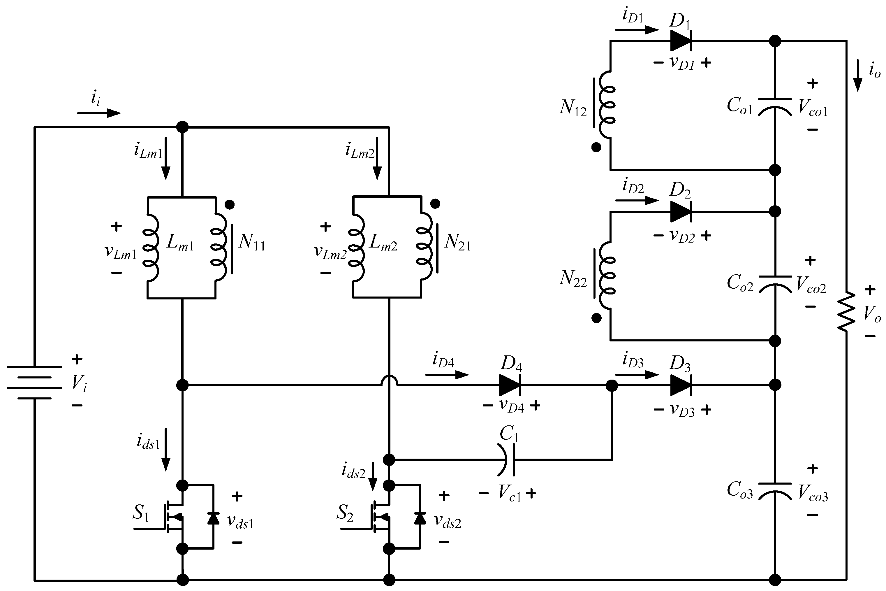
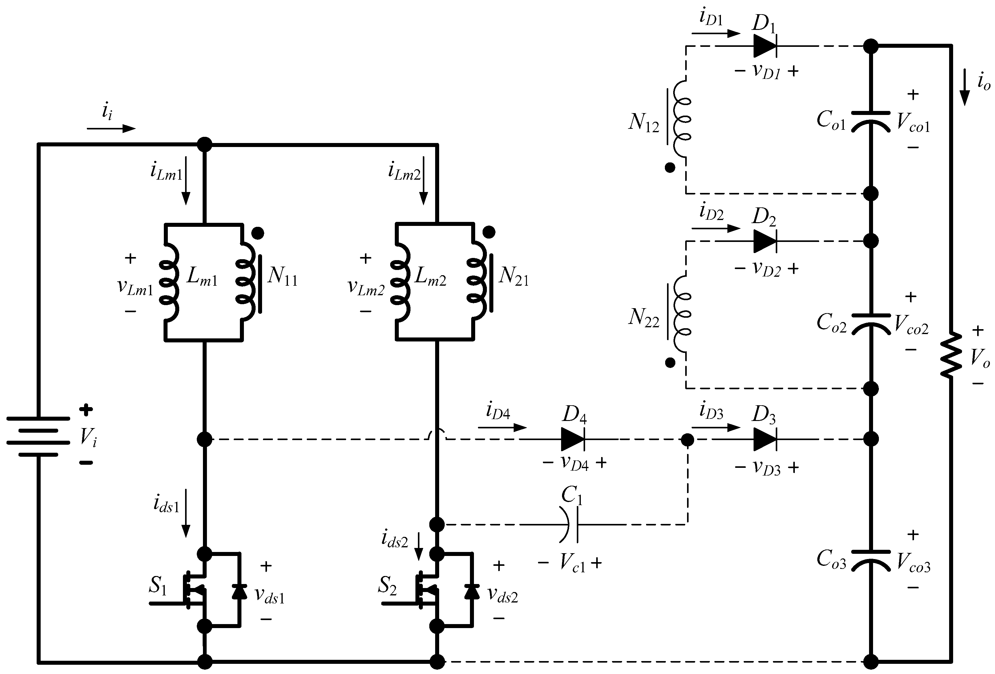
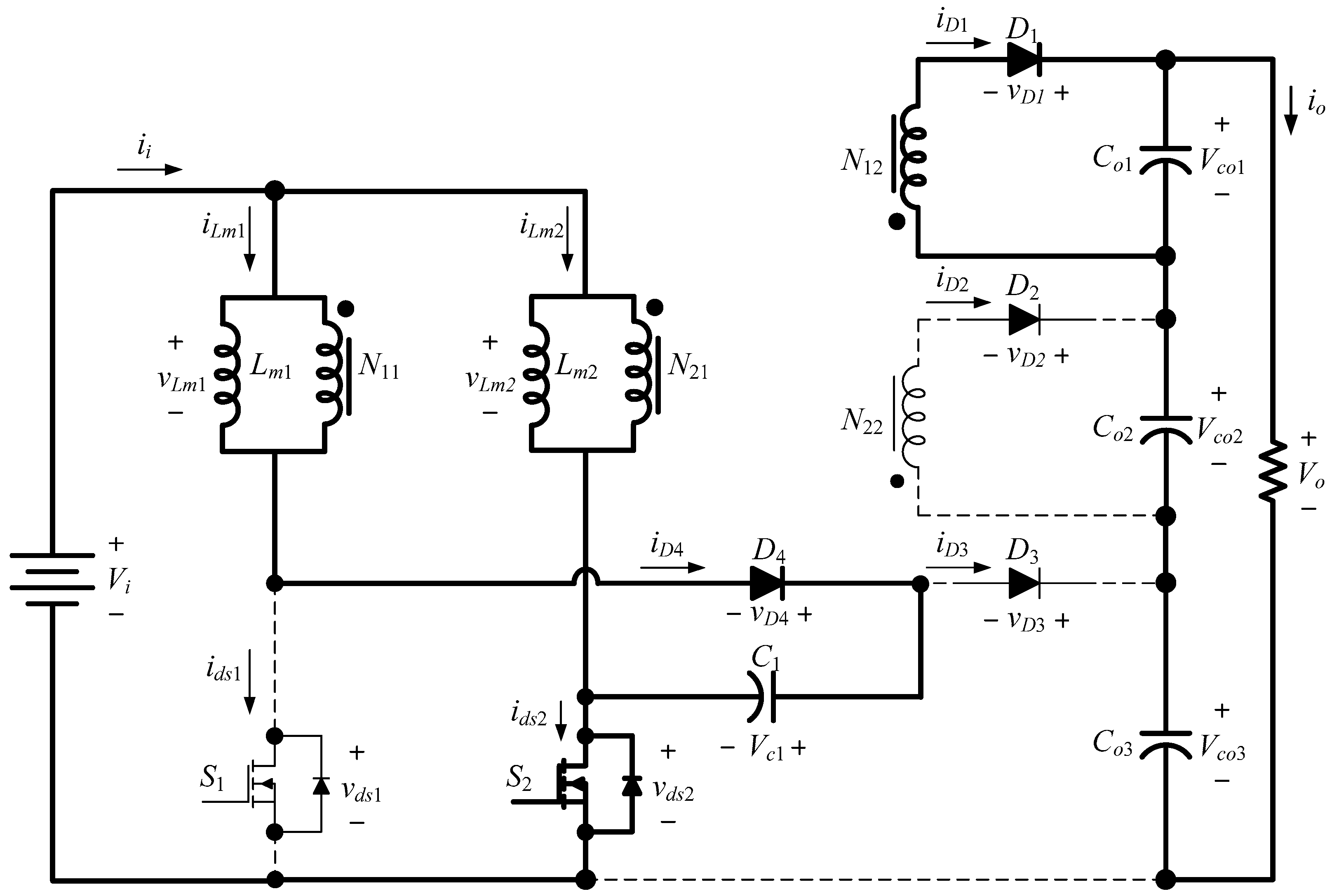
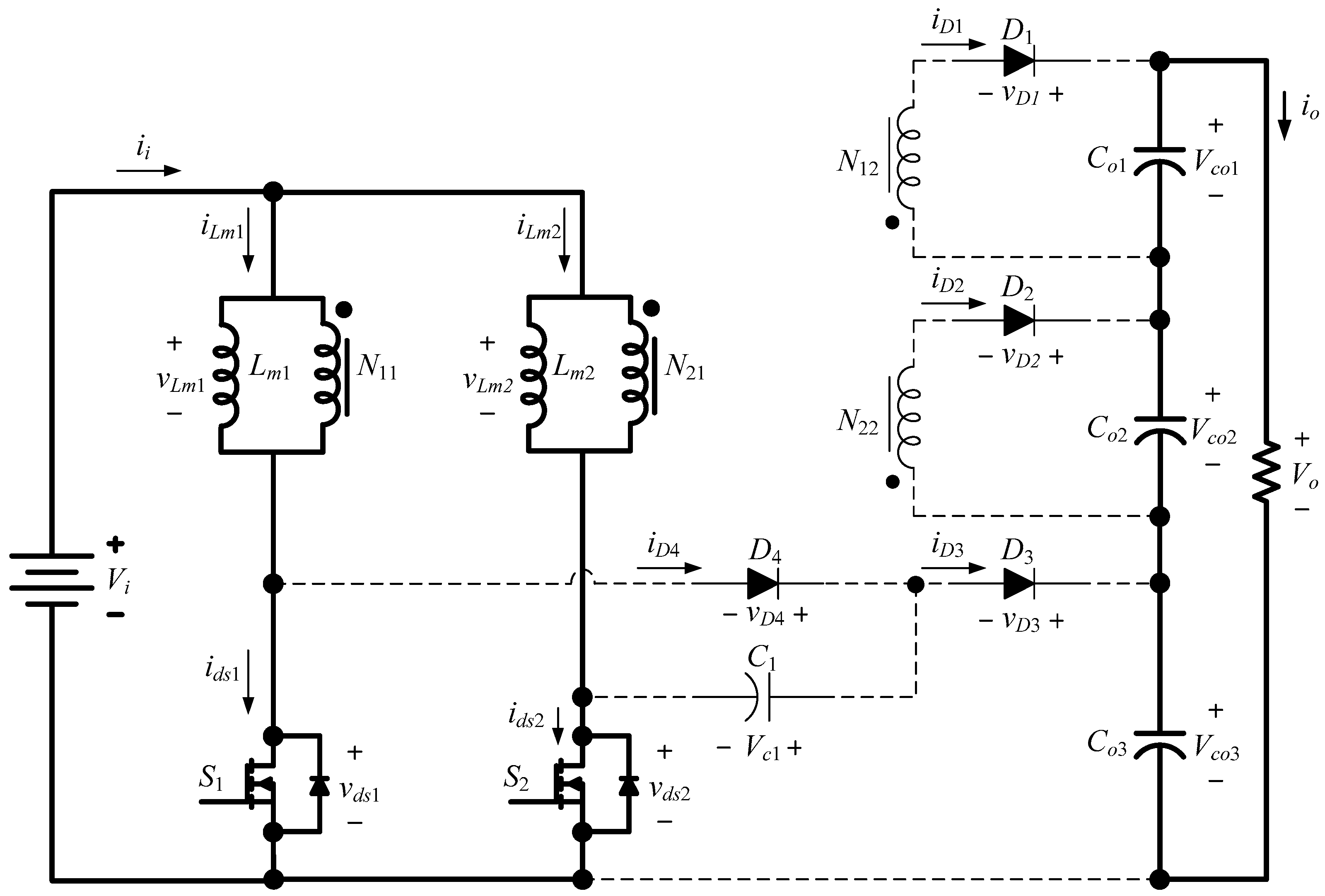
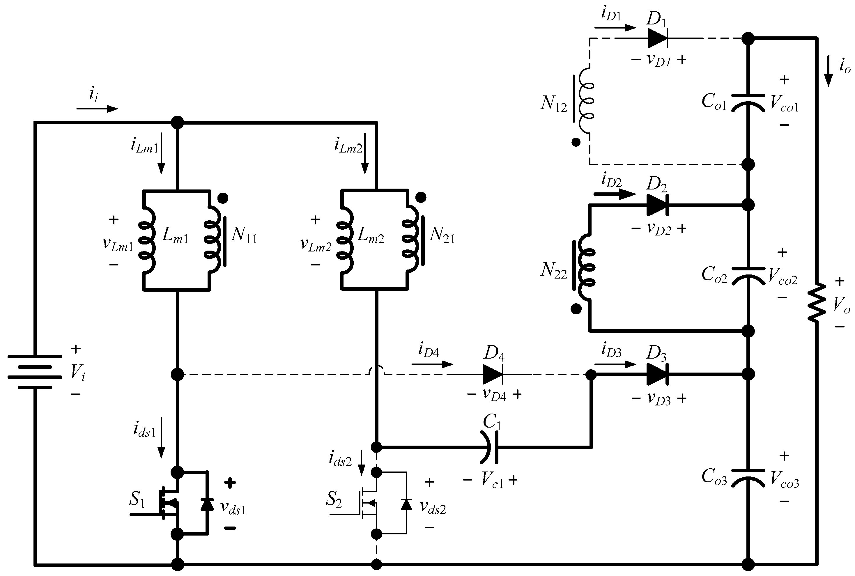
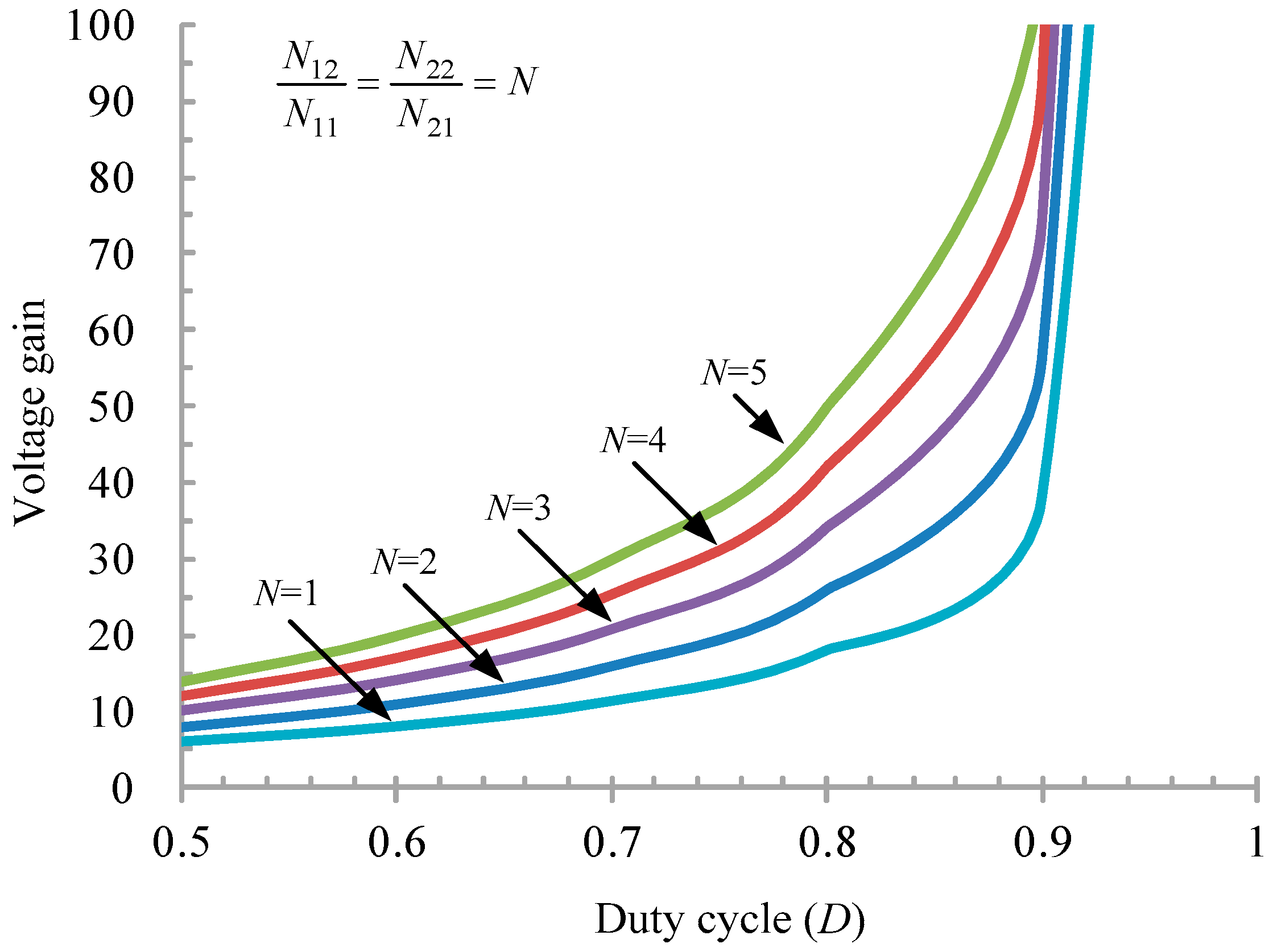
3. Inductor Coupled Interleaved Converter with High Voltage Conversion Ratio

As a low-voltage, high-current power source, a fuel cell requires a step-up converter for parallel operation with other types of power sources. Hence, this paper presents an interleaved inductor-coupled converter, as illustrated in Figure 1. It mainly involves a pair of boost converters, a flyback converter, and a clamp capacitor. Designed with a high voltage conversion ratio, this circuit configuration requires a low duty cycle, giving rise to a considerable reduction in the voltage ratings of power switches, in the conduction and switching loss of power switches. Besides, the input current ripple can be suppressed and the current rating of power switches can be reduced using an interleaving mechanism.
A good design of a boost converter with coupled inductor needs to achieve high voltage gain, low voltage and current ratings of switches, low voltage rating of diodes, and minimum additional elements. Table 2 lists the expected good design performance of the proposed boost converter with coupled inductors.

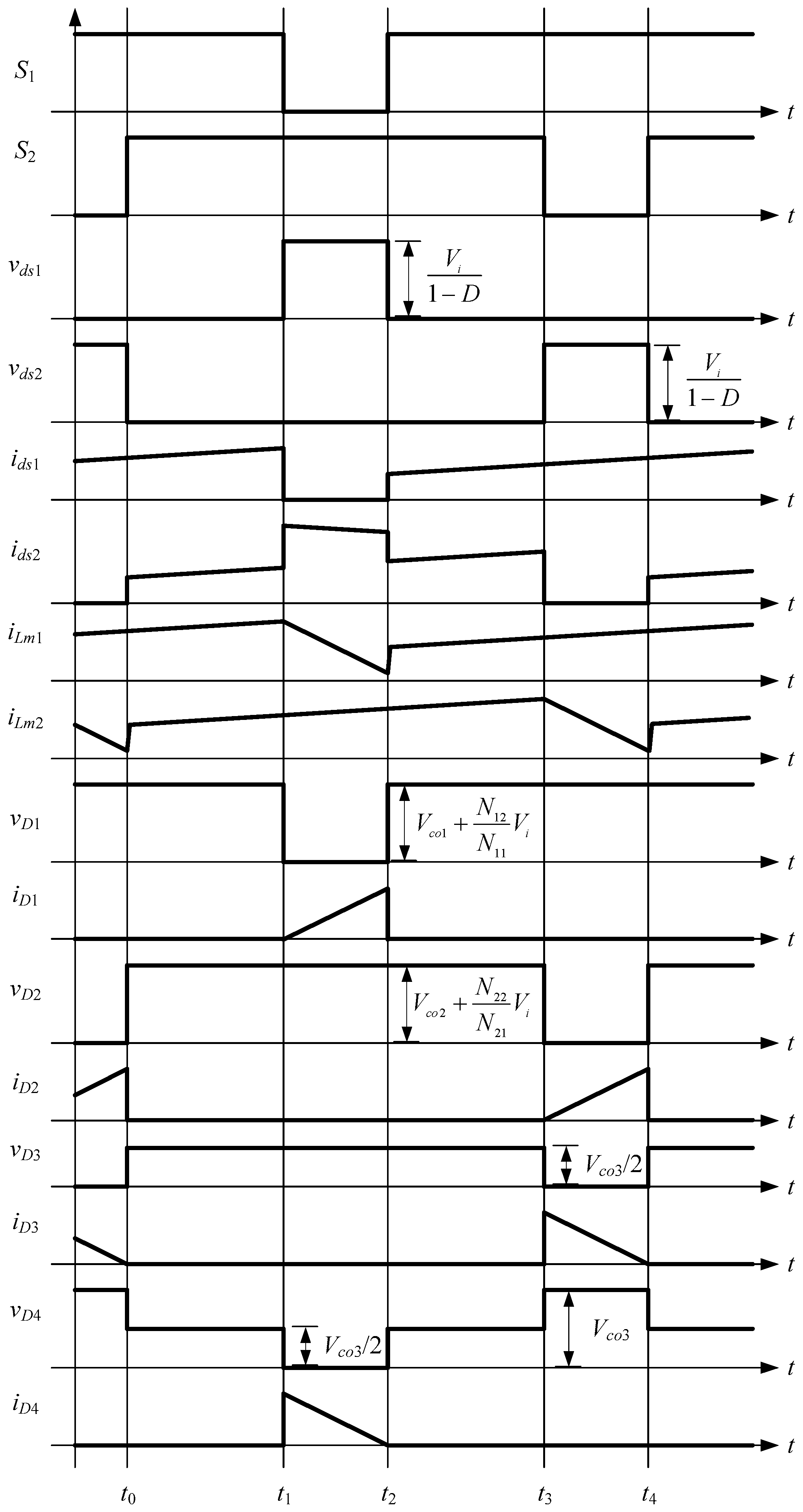
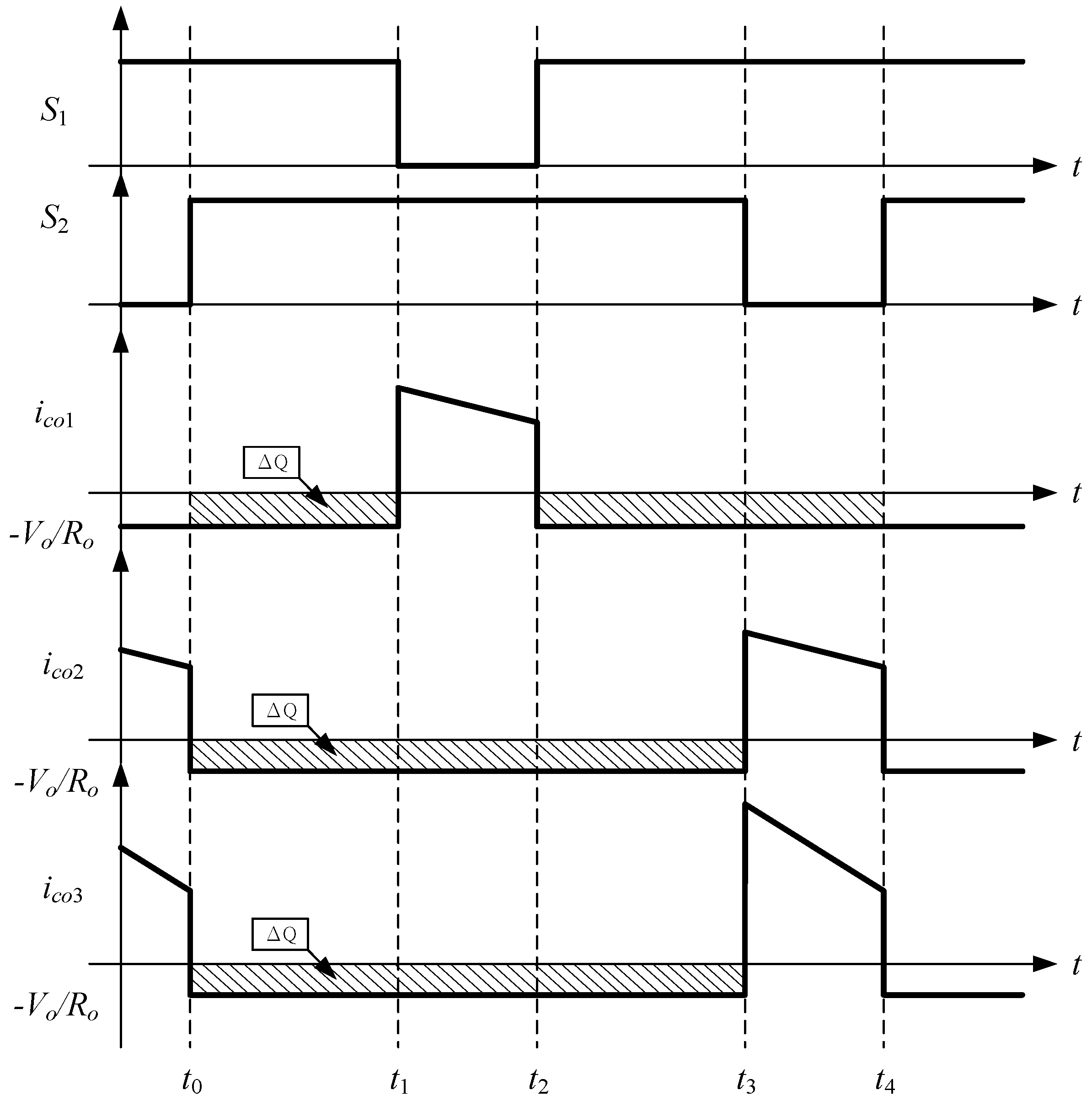
4. Operation Principle

This section is devoted to the mode analysis on the presented interleaved inductor-coupled converter. There are four operation modes involved in this converter, and the respective voltage and current waveforms across and through components are illustrated in Figure 2. For illustration purposes, the duty cycle is set to greater than 0.5 in continuous conduction mode (CCM), and the following assumptions are made.
(1)
All the components involved are ideal, meaning that the parasitic capacitance and the conduction resistance of each switch and the voltage drop across a forward-biased diode are not taken into account.
(2)
For simplification purposes, it is assumed that Lm1 = Lm2 = L, and iLm1 = iLm2. Hence, vLm1 = vLm2 = vL and iLm1 = iLm2 = iLm = 1/2ii.

4.1. Mode 1 (t0–t1)

The equivalent circuit in this mode is illustrated in Figure 3. Both S1 and S2 are switched on, and the input voltage Vi is applied to Lm1 and Lm2. With both inductors as energy storage devices, iLm1 and iLm2 rise linearly with time, expressed as:
L m 1 d i L m 1 d t = V i
L m 2 d i L m 2 d t = V i
The voltage drops across the reverse-biased diodes D1D4 are respectively described as:
v D 1 = V C o 1 + N 12 N 11 V i
v D 2 = V C o 2 + N 22 N 21 V i
v D 3 = V C o 3 V c 1
v D 4 = V c 1
The energy is released from the output capacitors Co1Co3 toward the load.

4.2. Mode 2 (t1–t2)

The equivalent circuit in this mode is illustrated in Figure 4. S1 is switched off, while S2 stays switched on. Meanwhile, iLm1 decreases linearly with time, formulated as:
L m 1 d i L m 1 d t = V i V c 1
The stored inductive energy is released by way of D4 to the clamp capacitor C1. In the same manner, the energy is released via D1 to the output capacitor Co1 due to the reversed polarity of N12, and the output voltage across Co1 is expressed as:
V C o 1 = N 12 N 11 ( V c 1 V i )
Furthermore, Lm2 serves as an energy storage device as in Mode 1, and iLm2 is given as:
L m 2 d i L m 2 d t = V i
The voltage drops across the reverse-biased diodes D2 and D3 are respectively expressed as:
v D 2 = V C o 2 + N 22 N 21 V i
v D 3 = V C o 3 V c 1

4.3. Mode 3 (t2–t3)

The equivalent circuit in this mode is illustrated in Figure 5. As in Mode 1, S1 and S2 both are switched on, and the input voltage Vi is applied to the inductors Lm1 and Lm2. Consequently, the currents through inductors, as given in Equations (1) and (2), rises linearly with time, and all the diodes are reverse-biased, as described in Equations (3)–(6). Hence, the electricity is delivered from Co1Co3 to the load.

4.4. Mode 4 (t3–t4)

The equivalent circuit in this mode is illustrated in Figure 6. S1 remains switched on, while S2 is switched off. In the meantime, iLm1 and iLm2 rises and decreases linearly with time respectively, described as:
L m 1 d i L m 1 d t = V i
L m 2 d i L m 2 d t = V i + V c 1 V C o 3
Electricity is released to Co3 via C1 and D3, owing to a reversal of the voltage polarity across Lm2. Likewise, the energy is released to Co2 by way of D2 due to the voltage polarity reversal across N22, and the voltage drop across Co2 is expressed as:
V C o 2 = N 22 N 21 ( V C o 3 V c 1 V i )
The voltage drops across D1 and D4 are respectively expressed as:
v D 1 = V C o 1 + N 12 N 11 V i
v D 4 = V C o 3
Following the inductor volt second balance principle, the combined use of Equations (1), (2), (7), and (13) gives:
V i D T + ( V i V c 1 ) × ( 1 D ) T = 0
V i D T + ( V i + V c 1 V C o 3 ) × ( 1 D ) T = 0
Back substitution of Equation (17) into Equation (18) now gives:
( V i + V c 1 + V i + V c 1 V C o 3 ) × ( 1 D ) T = 0
Rearrangement of Equation (19) gives the voltage drop across the clamp capacitor:
V c 1 = V c o 3 2
Substitution of Equation (20) into either Equation (18) or Equation (19) gives the voltage drop across the output capacitor Co3:
V C o 3 = 2 V i 1 D
VCo1VCo3 are summed as the total output voltage, formulated as:
V o = V C o 1 + V C o 2 + V C o 3
Substitution of Equations (8), (14), and (21) into Equation (22) gives:
V o = N 12 N 11 D V i 1 D + N 22 N 21 D V i 1 D + 2 V i 1 D
or, expressed in a concise form:
V o = [ ( N 12 N 11 + N 22 N 21 ) D + 2 ] 1 D V i
As a graphic representation of Equation (24), a family of voltage gain-duty cycle curves is illustrated in Figure 7, with N = N12/N11 = N22/N21 as a parameter.

5. Performance Comparison
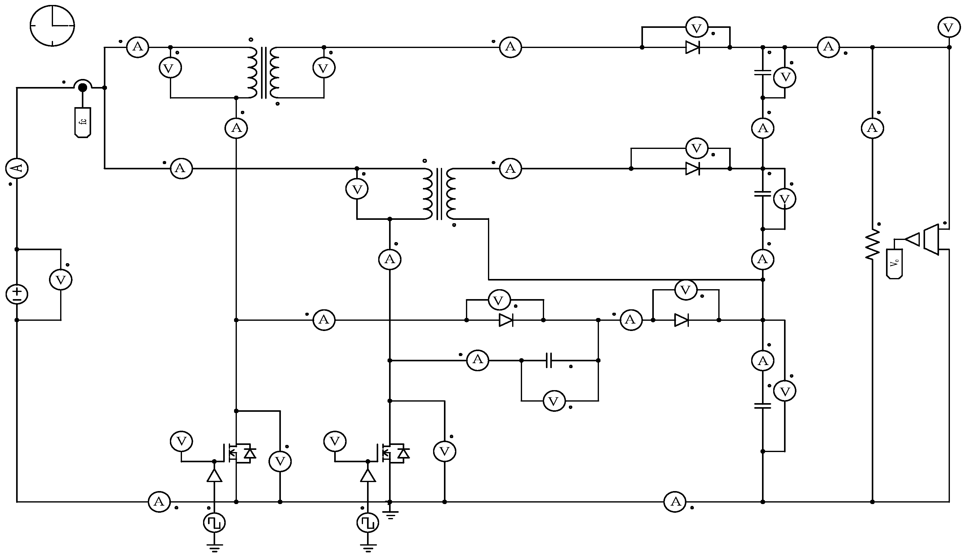
To demonstrate the performance superiority of this work, Table 3 gives a comparison on the voltage gain, voltage/current ratings of power switches, voltage rating of diodes, and the numbers of the required inductors, capacitors, and diodes in this proposal and other representative pieces of work [4,17,19,22,23,24,25].
As can be seen in Table 3, the presented converter is found to outperform its counterparts in terms of the number of components required and the voltage ratings of switches and diodes. It also meets the expected performance listed in Table 2.

6. Converter Design

The presented interleaved inductor-coupled converter is developed as a combined form of a boost converter and a flyback one. Table 4 lists the electrical specifications of the boost converter.
(1) Choice of inductance
Turns ratio of Lm1 to Lm2 is specified as 1:2 herein, and then substituted into Equation (24), simplified as:
V o = V i [ 4 D + 2 ] 1 D
For simplification purposes, the inevitable power loss in each component is not taken into account, meaning that the input power completely reaches the output of the converter, i.e.,
V i × 2 I L m ( a v g ) = P o
Substitution of the turns ratio and Equation (24) into Equation (26) gives the average inductor current:
I L m ( a v g ) = P o 2 V i = V i [ 4 D + 2 ] 2 2 ( 1 D ) 2 R
As illustrated in Figure 2, the maximum and minimum currents through Lm1 and Lm2 can be expressed in terms of the average value and the current swing, respectively, as:
I L m 1 , 2 ( m a x ) = P o 2 V i + 1 2 V i D T L m
I L m 1 , 2 ( m i n ) = P o 2 V i 1 2 V i D T L m
For operation in CCM, it is requested that ILm1,2(min) be greater than zero, that is,
I L m ( m i n ) = P o 2 V i 1 2 V i D T L m 0
Rearrangement of Equation (30) gives the lower bound of inductance:
L m ( m i n ) V i 2 D P o f
Designed to operate in CCM under a light load of 300 W, the presented converter must drive a 400 Ω load. Accordingly, Equations (24) and (31) give a duty cycle (D) of 0.78 and a minimum inductance of 23 µH, respectively. In consideration of redundancy, a 35 µH inductor is employed herein.
(2) Choice of capacitance
In the vast majority of DC/DC converters, the output is followed by a shunt capacitor as a way to reduce the output ripple voltage caused by on/off switching. With Co1 = Co2 = Co3 = Co, as illustrated in Figure 8, it is observed that iCo1iCo3 share the same waveform, and the change of charge is given as:
| Δ Q | = ( V o R o ) D T = C o Δ V o
Rearrangement of Equation (32) gives:
C o = D ( Δ V o / V o ) R o f
Under arbitrary load conditions, substitution of a ripple ratio below 0.5% to Equation (33) gives Co = 50 µF. Hence, a commercially available 470 µF/450 V capacitor is employed herein.
The above analysis indicates an equivalent impedance of 122.5 Ω and an output voltage of approximately 15 V at an output power of 1000 W in a fuel cell. Substitution of the above results into Equation (24) gives D = 0.78, and Equation (28) results in ILm1,2(max) ≈ 41 A. Furthermore, Figure 2 illustrates the waveforms of the current through and the voltage drop across the power switches and the diodes, according to which commercially available IGBT MMG100J030U (600 V/100 A) switches (IXYS, Milpitas, CA, USA) and IQBD30E60A1 (600 V/60 A) diodes (IXYS, Milpitas, CA, USA) are employed herein.

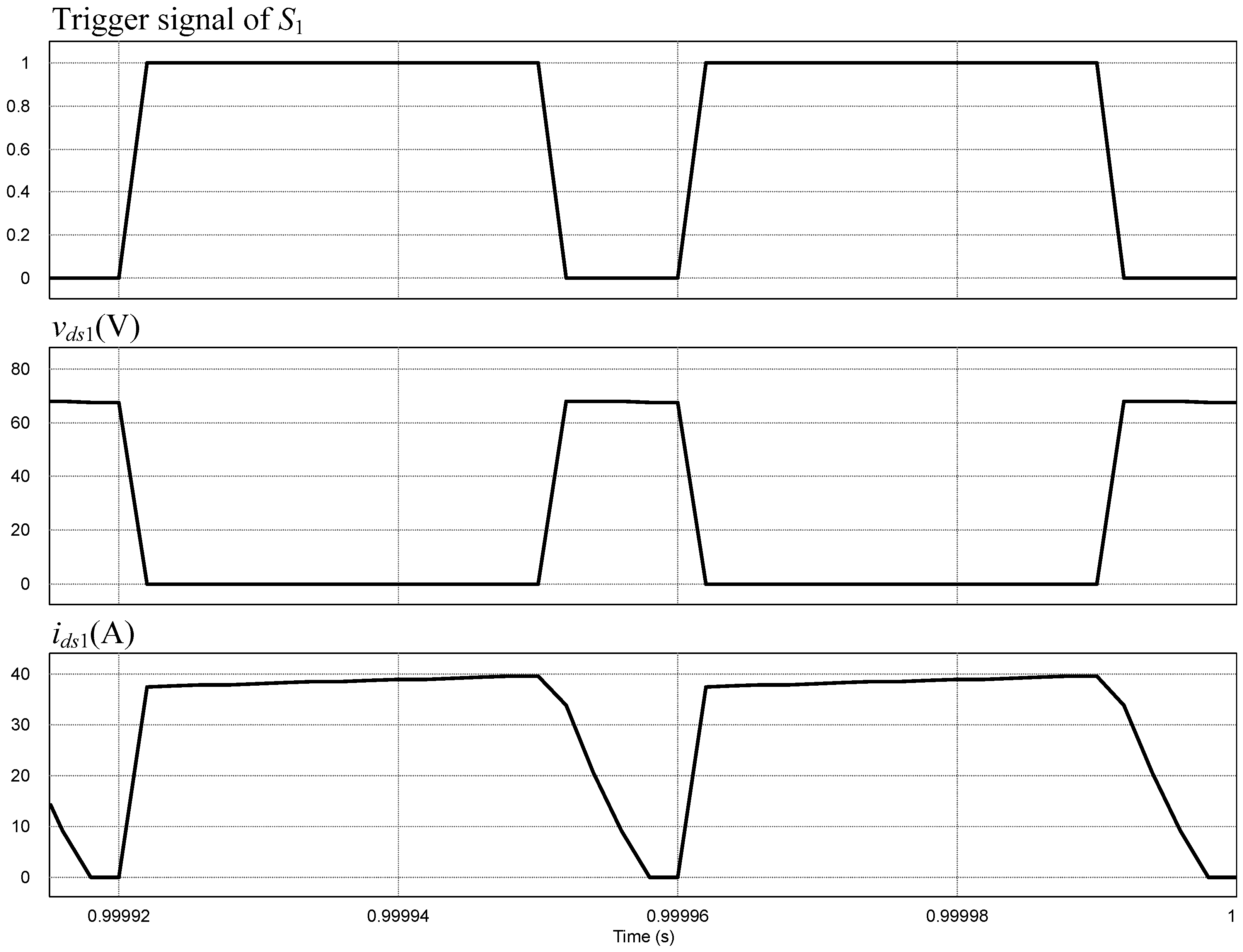
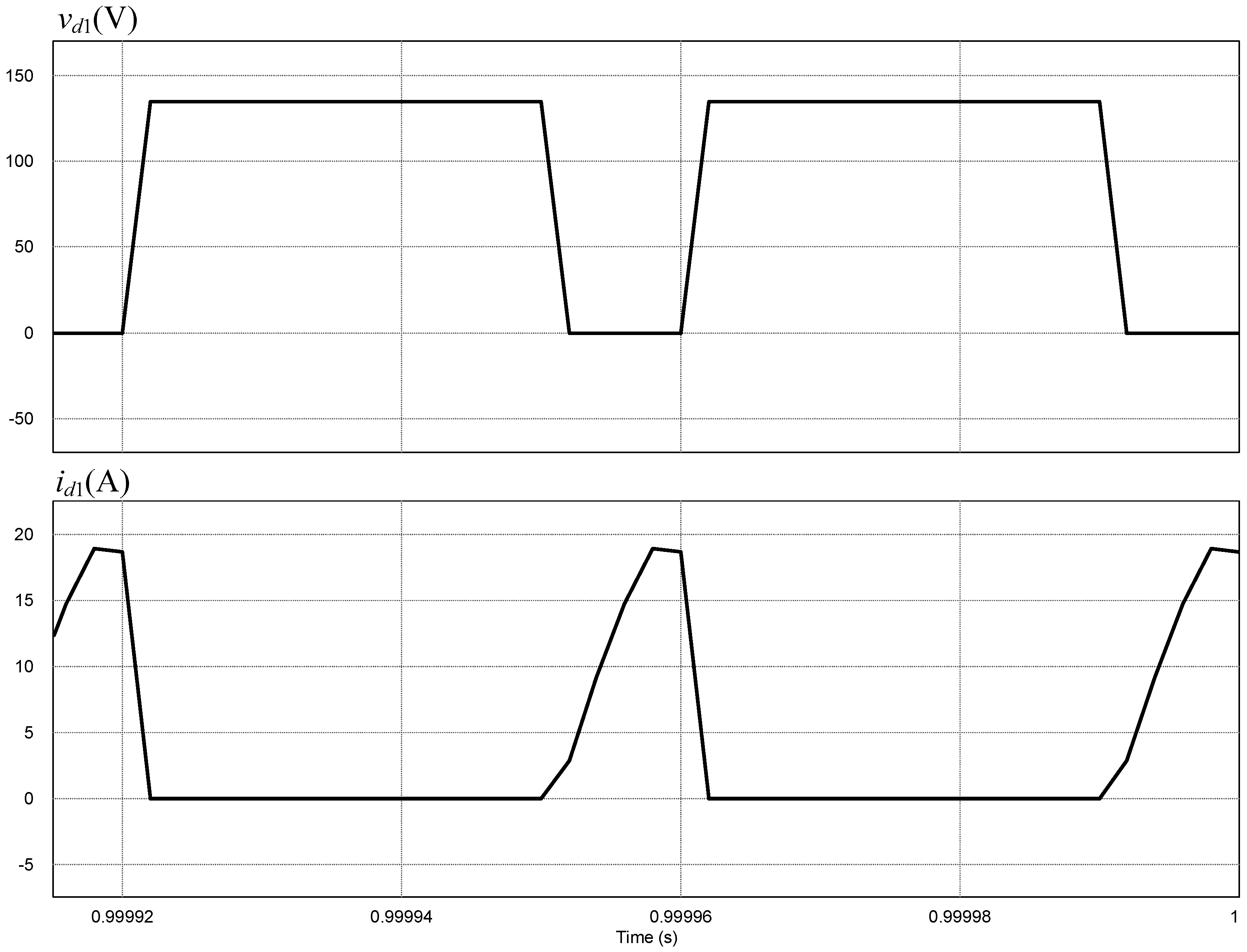
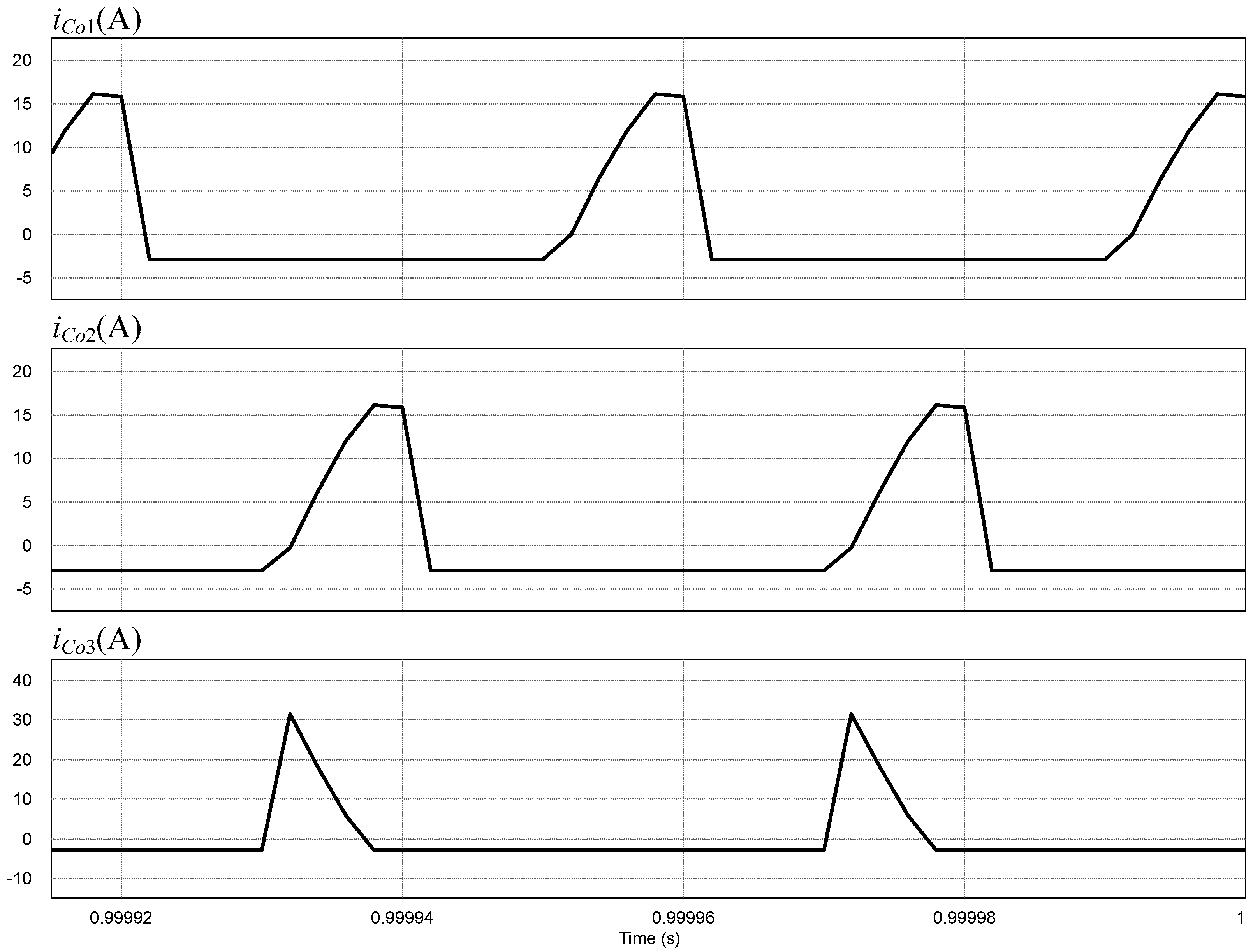
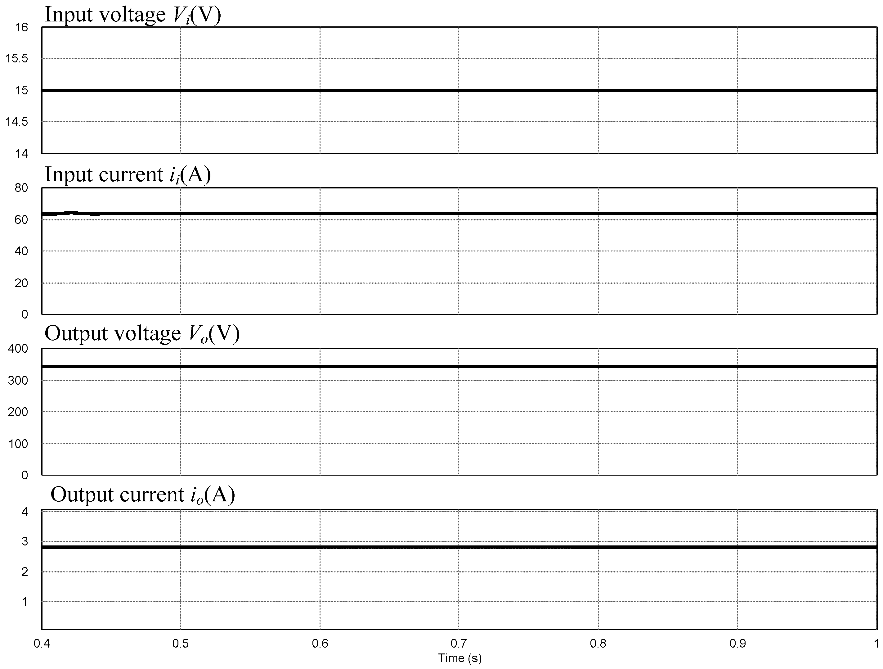
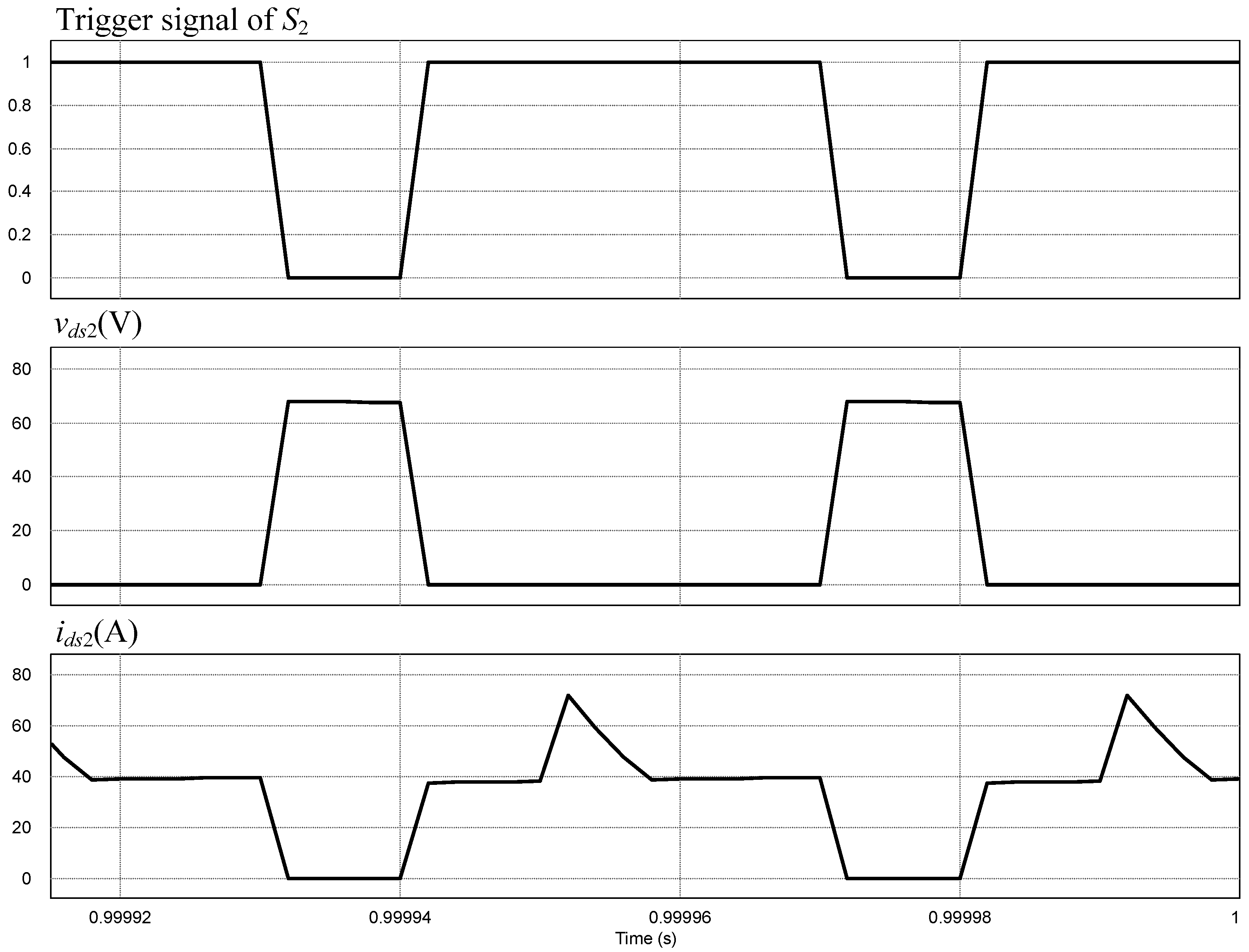
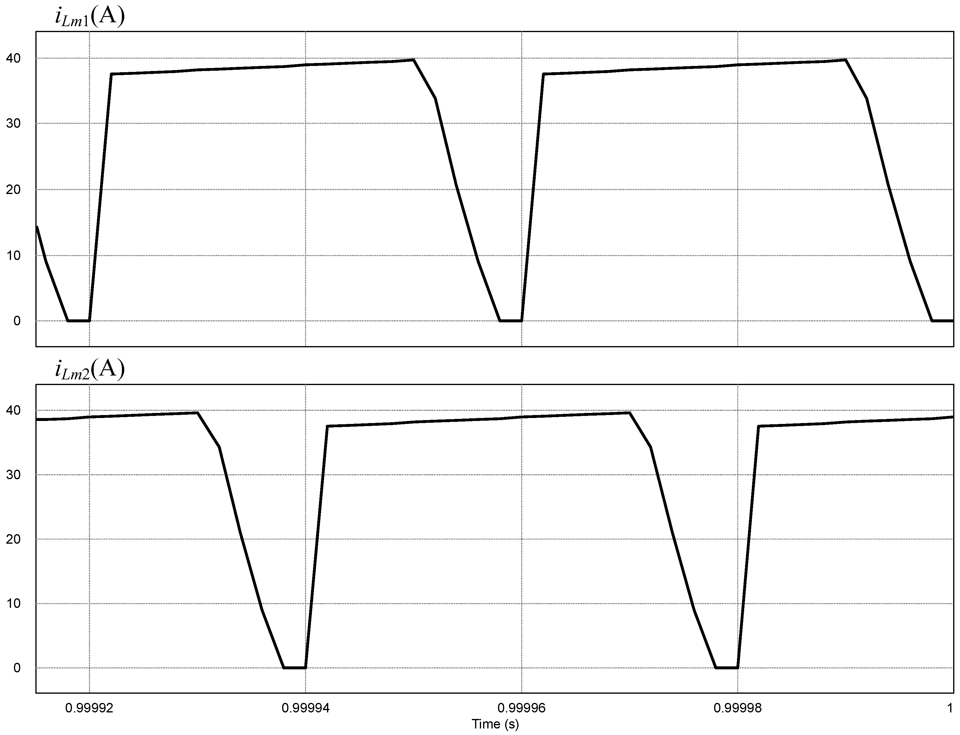
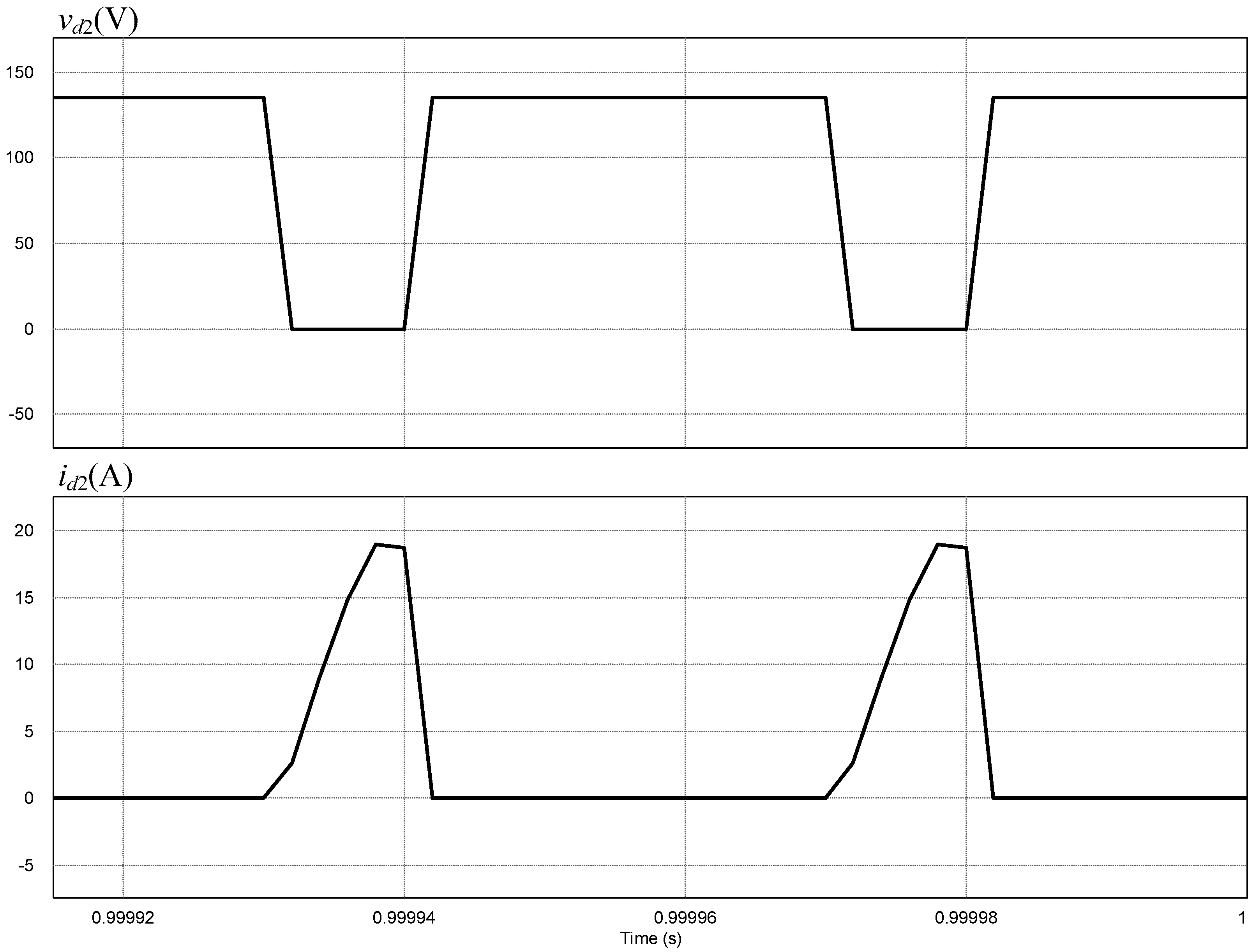
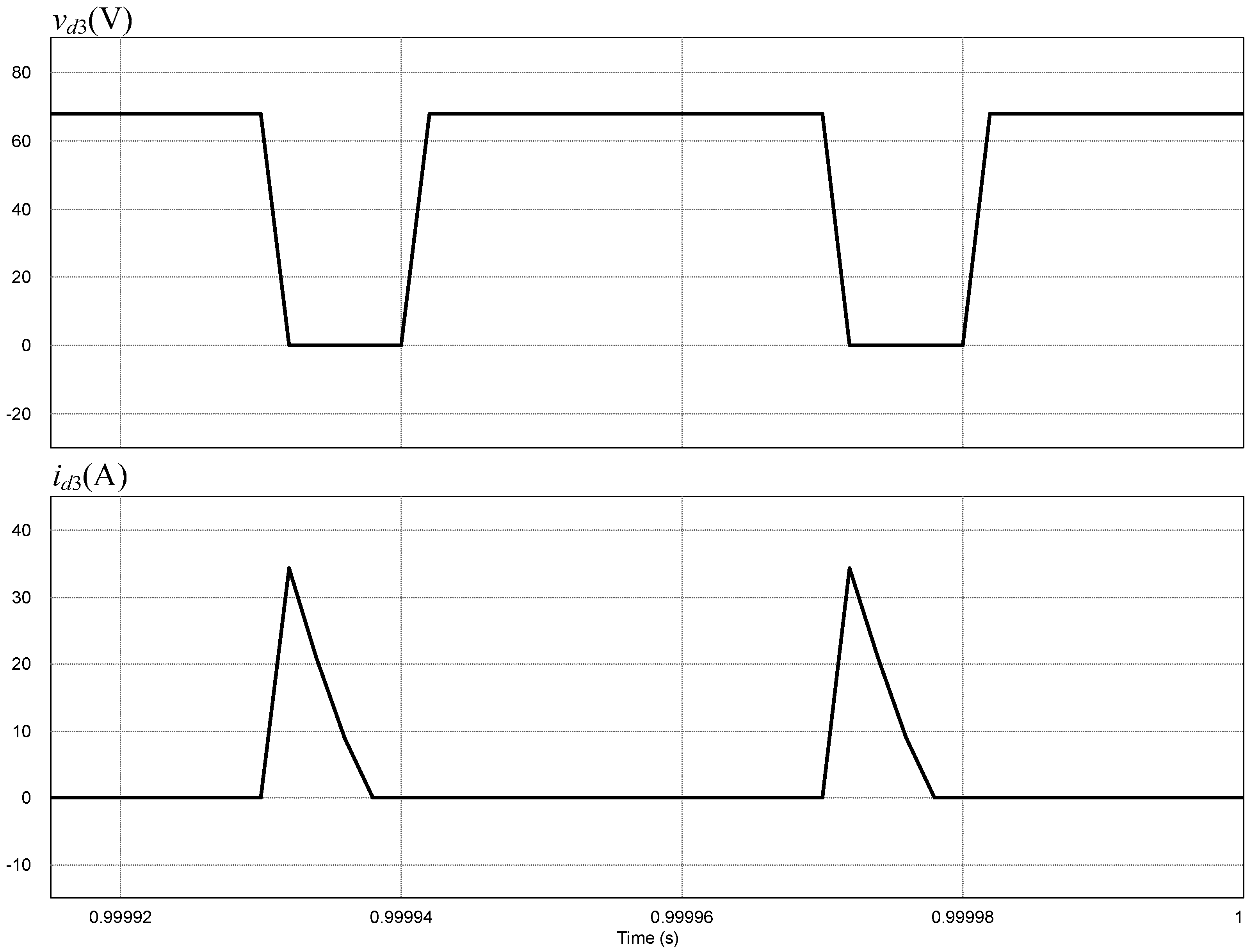
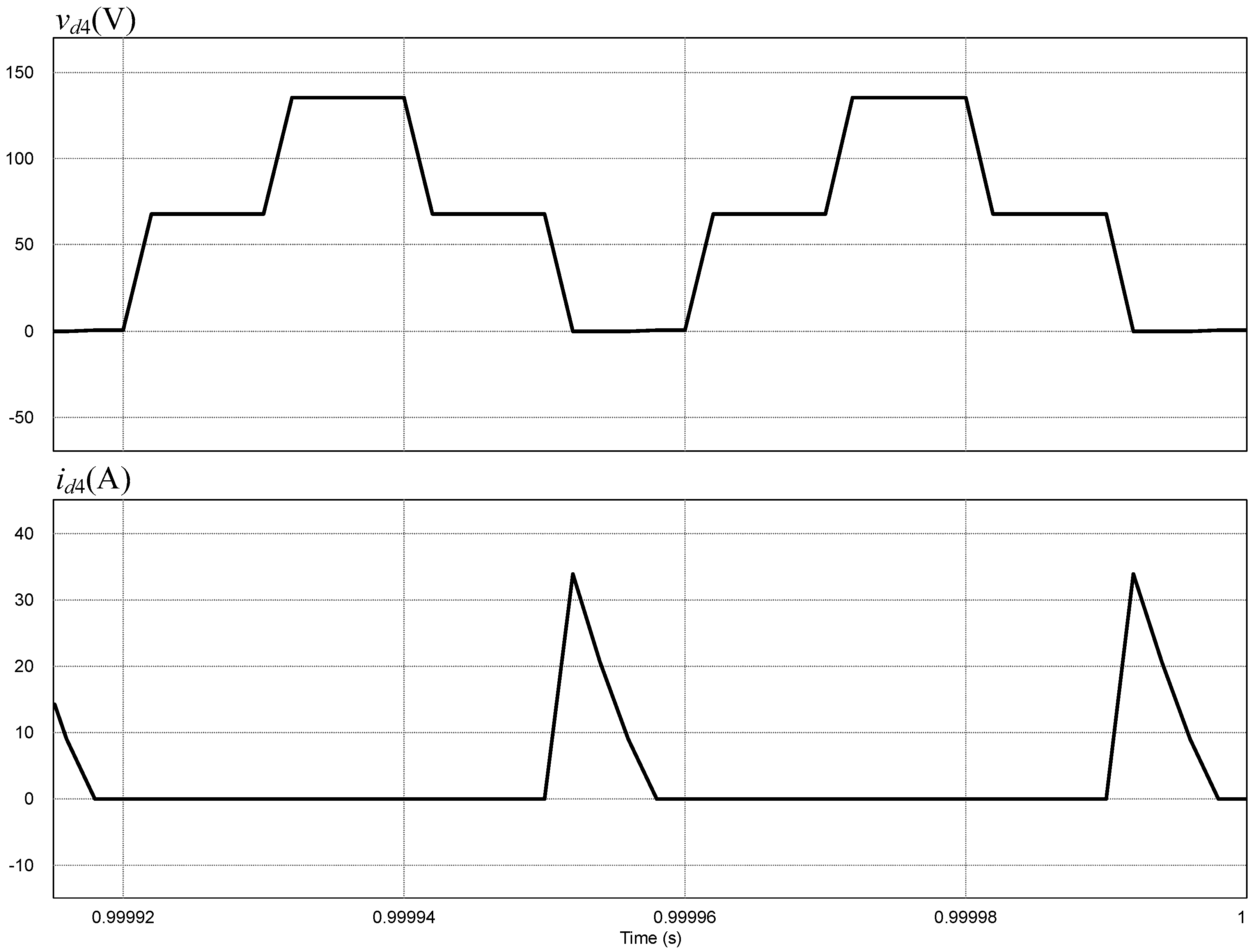
7. Simulation Results

Power simulation (PSIM) software simulations are conducted on an interleaved inductor-coupled converter with a high voltage conversion ratio as illustrated in Figure 9. With a fuel cell output voltage of 15 V, illustrated in Figure 10 are the simulated input and output voltage/current waveforms of the presented DC/DC converter at an output voltage of 350 V and an output power of 1000 W. Exhibited in Figure 11 and Figure 12 are the simulated waveforms of the trigger signals for S1 and S2, the currents through the diodes ids1 and ids2 and the voltage drops across the power transistors vds1 and vds2. Presented in Figure 13 are the simulated waveforms of the currents through the coupled inductors Lm1 and Lm2, while in Figure 14, Figure 15, Figure 16 and Figure 17 are the simulated voltage/current waveforms across/through the diodes D1D4, and in Figure 18 are the simulated current waveforms through the capacitors iCo1iCo3. A good agreement is found between all the above-stated simulation results and Figure 2.

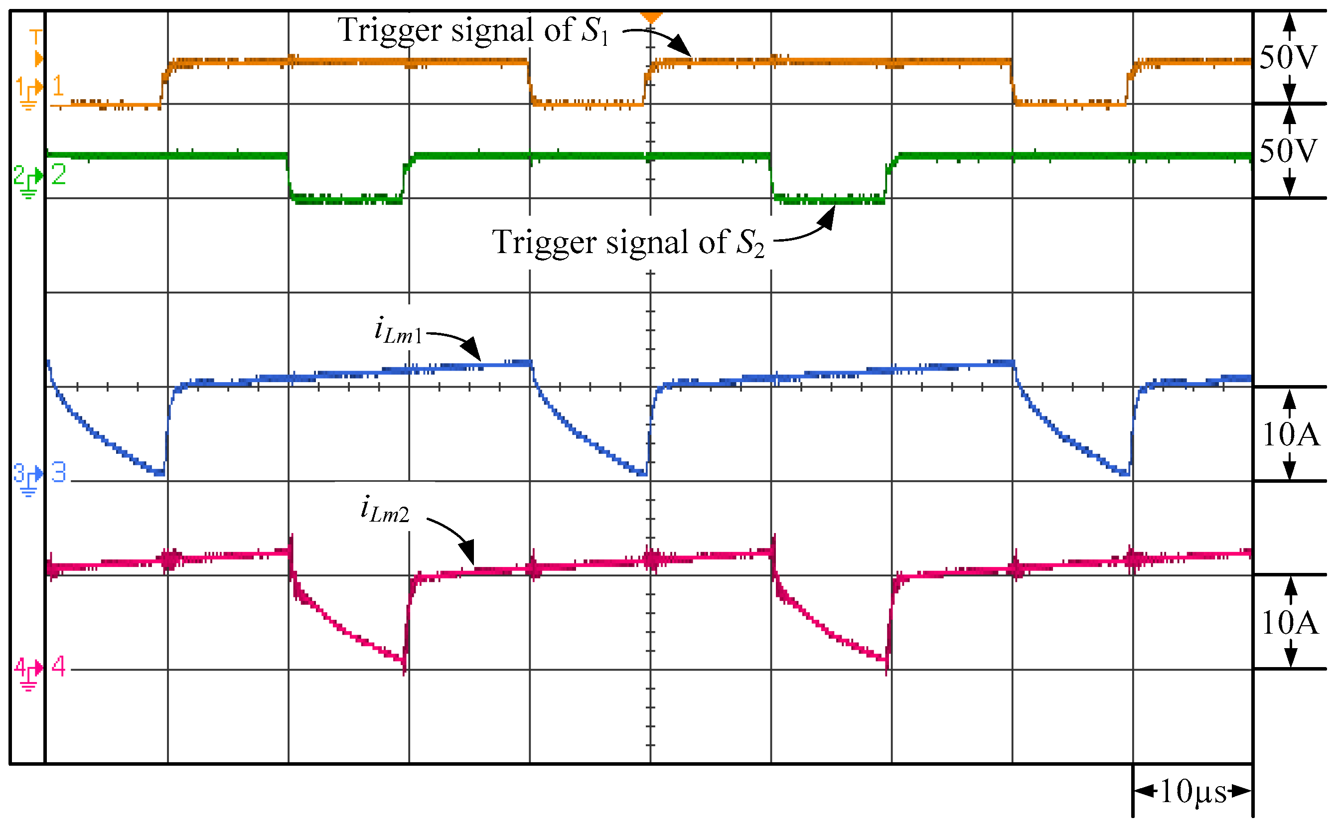
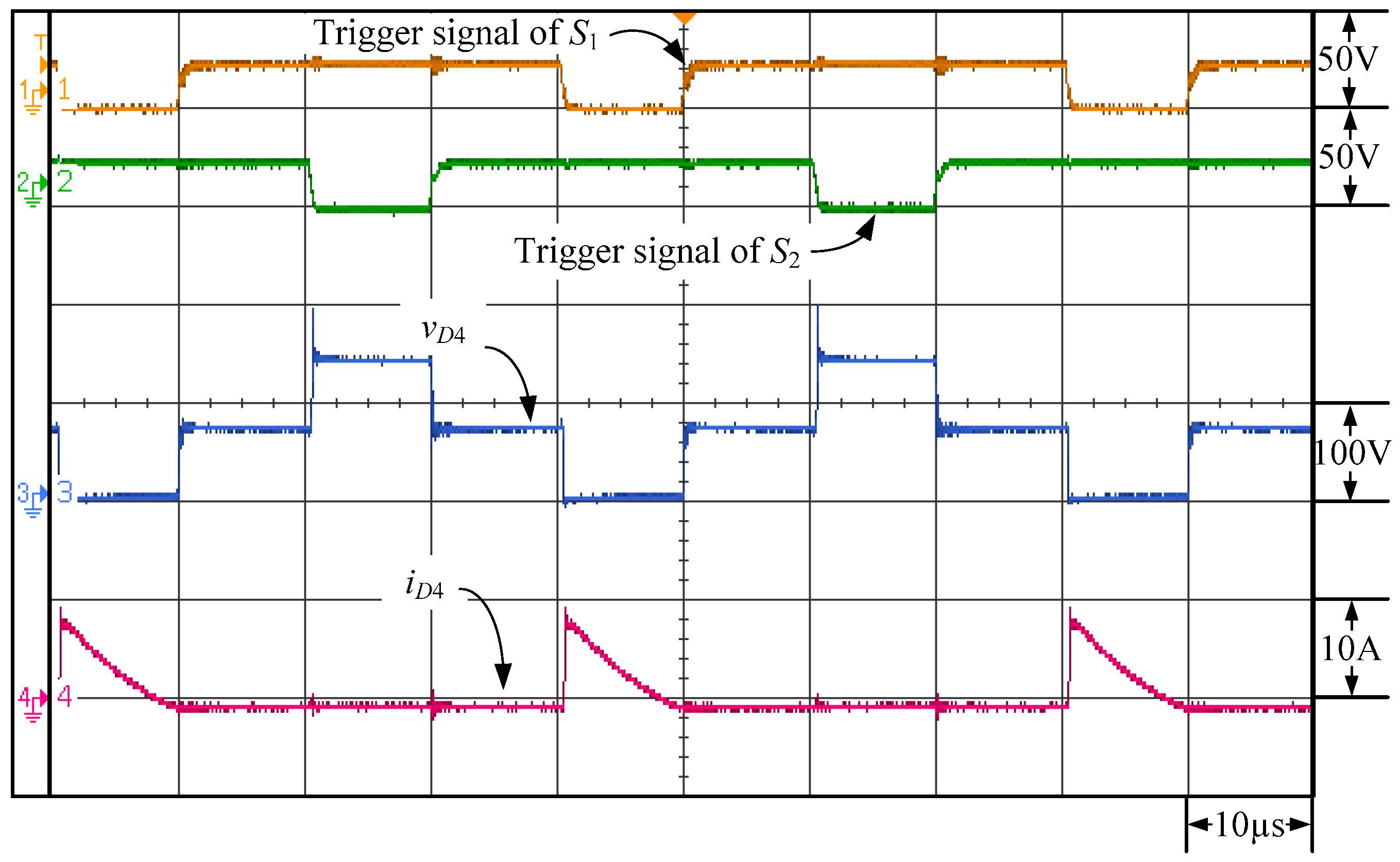
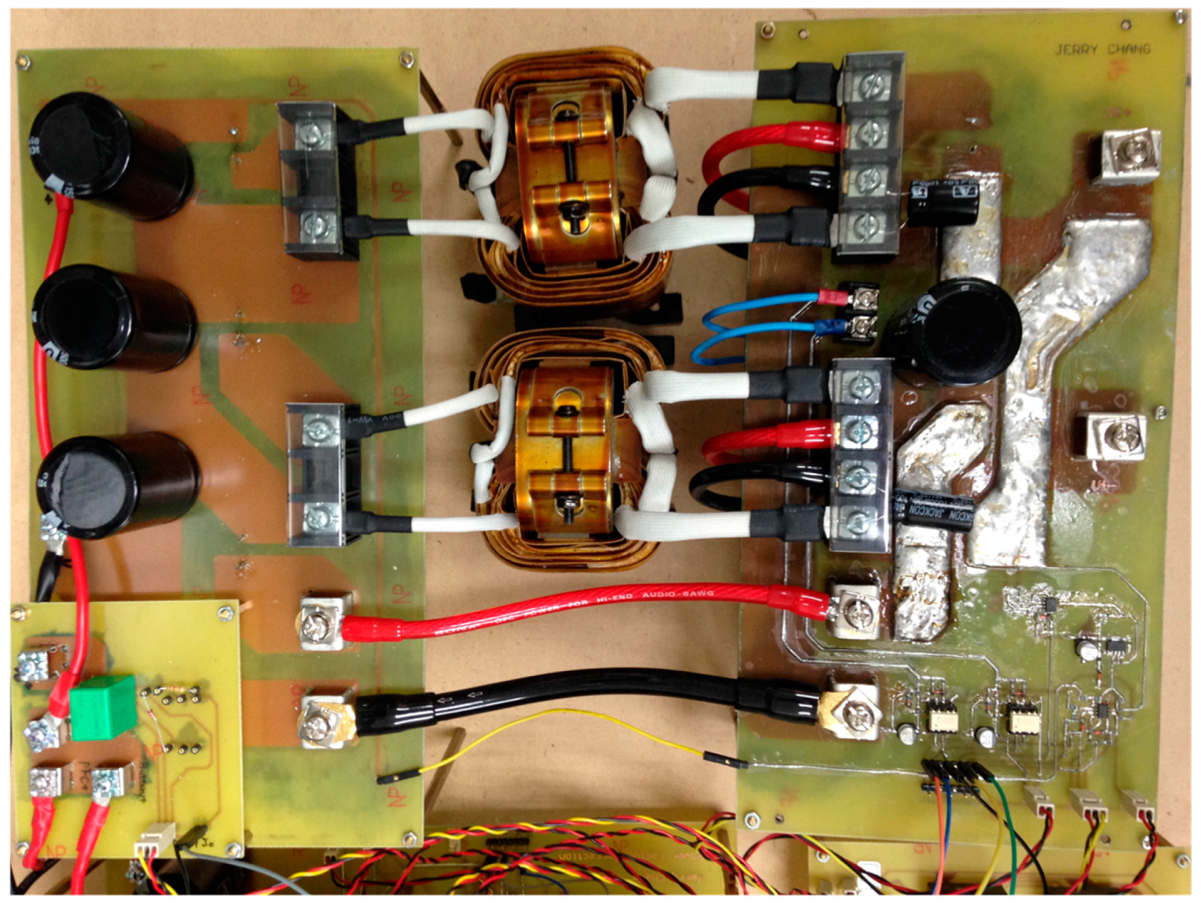
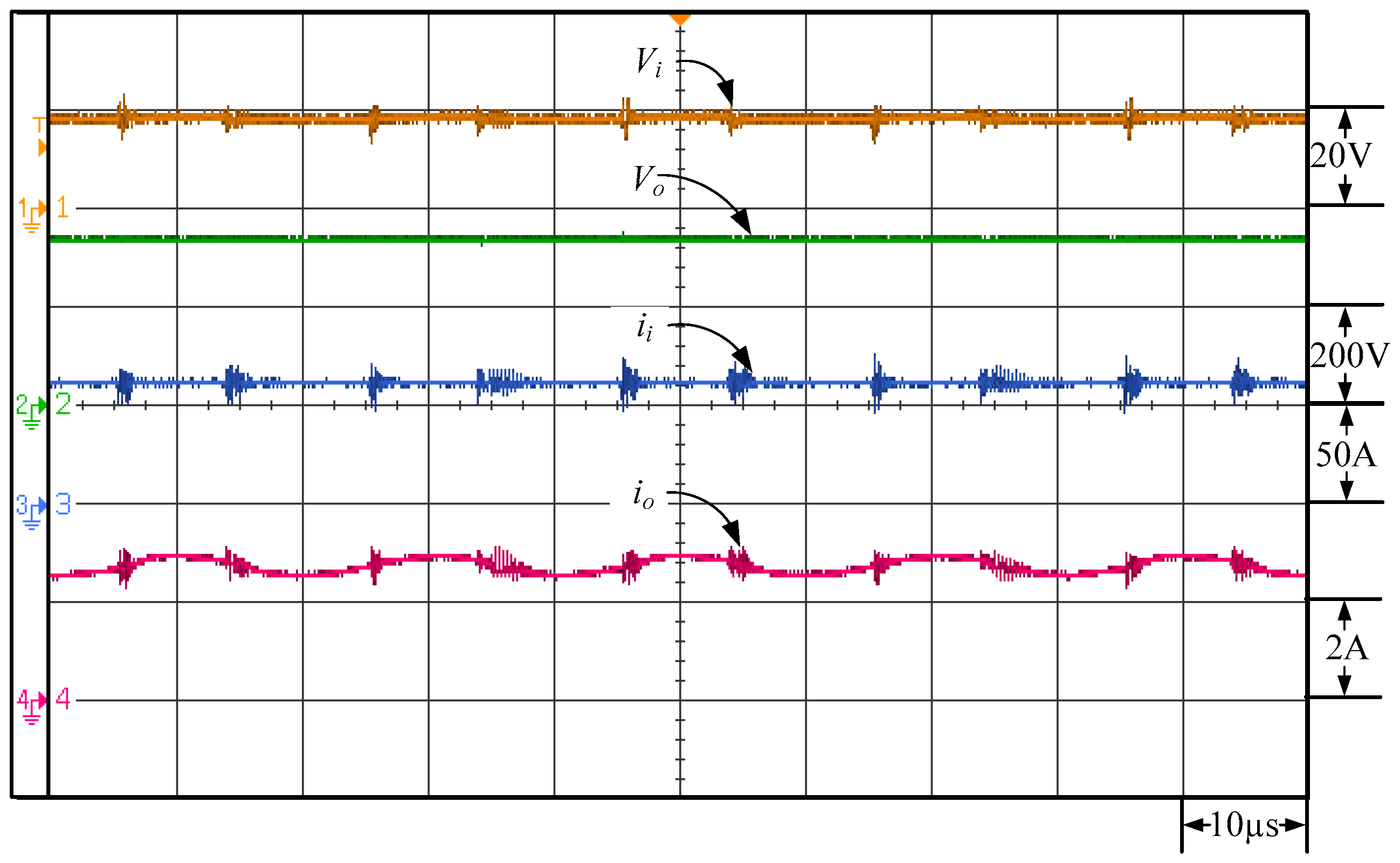
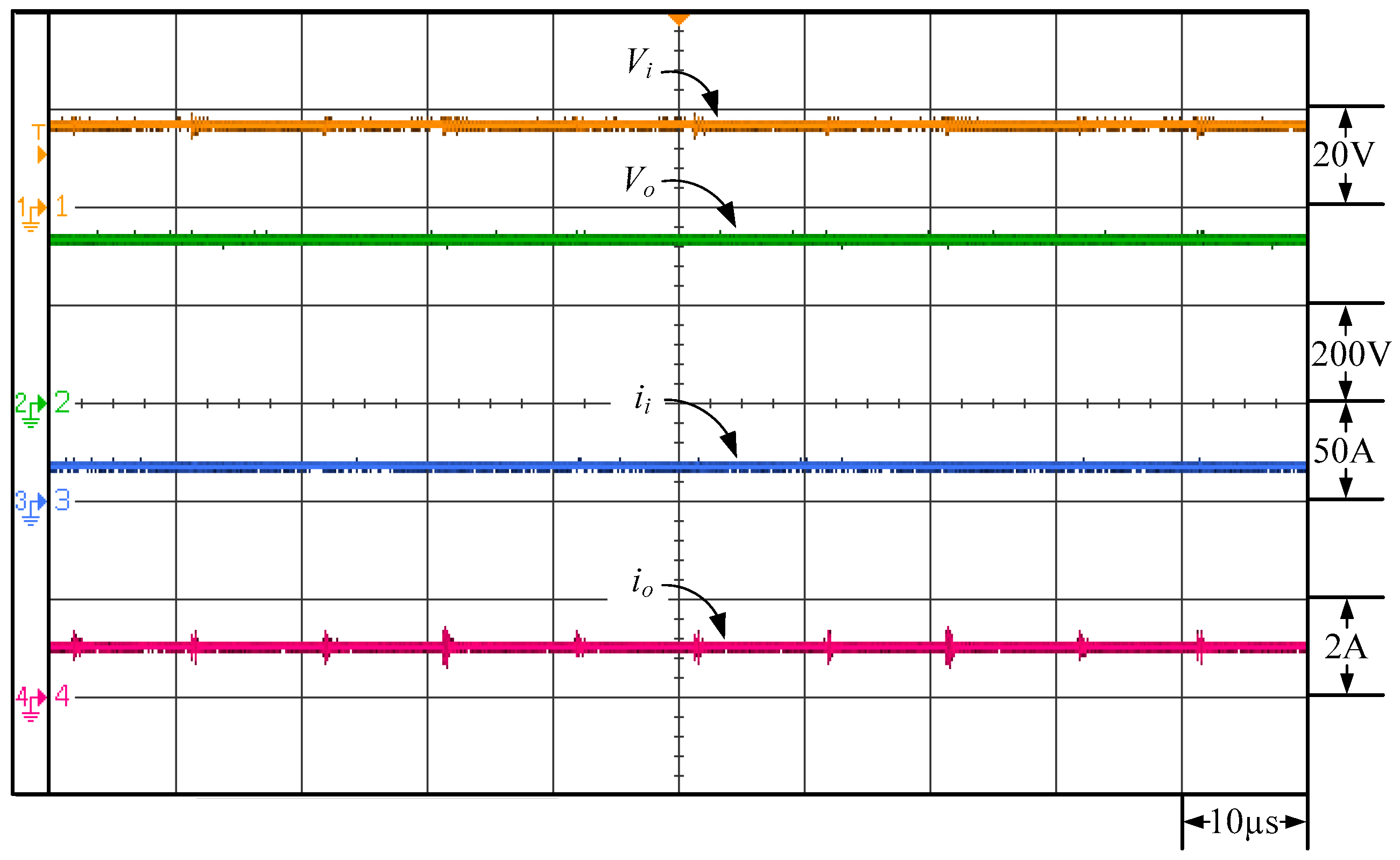
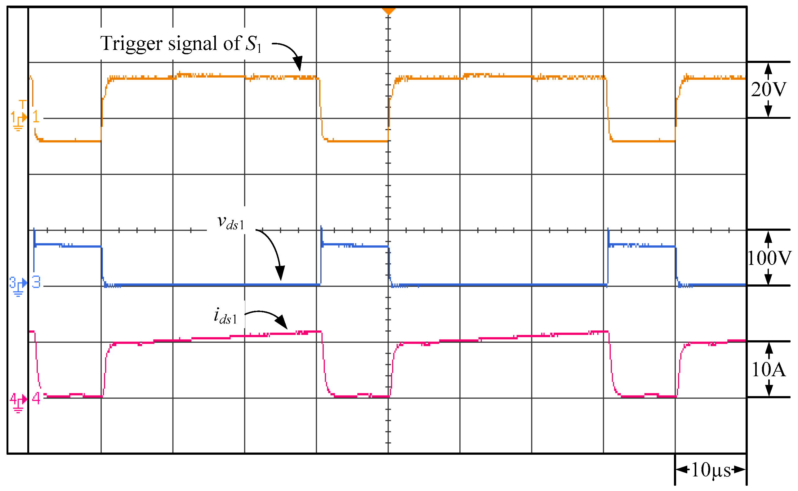
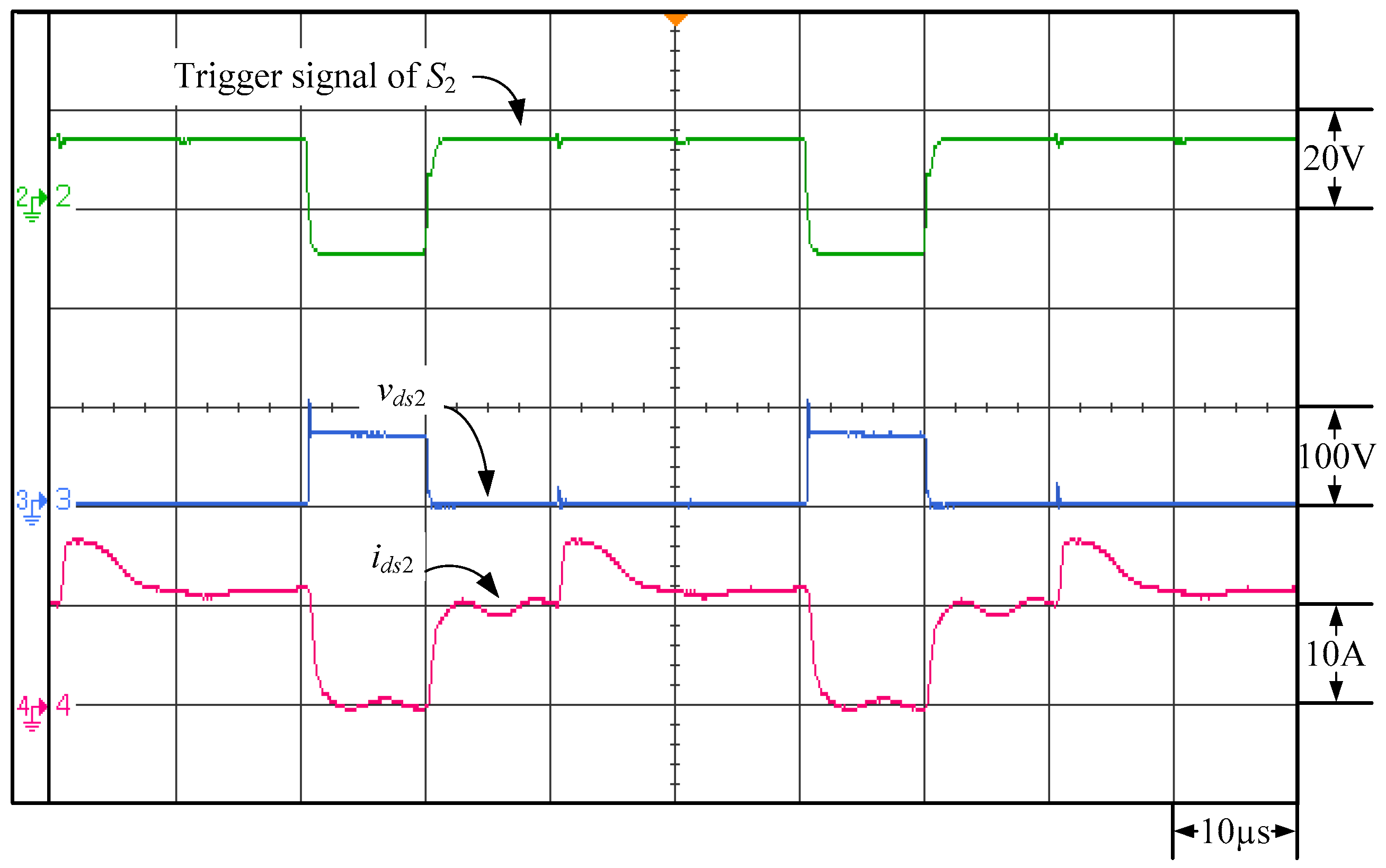
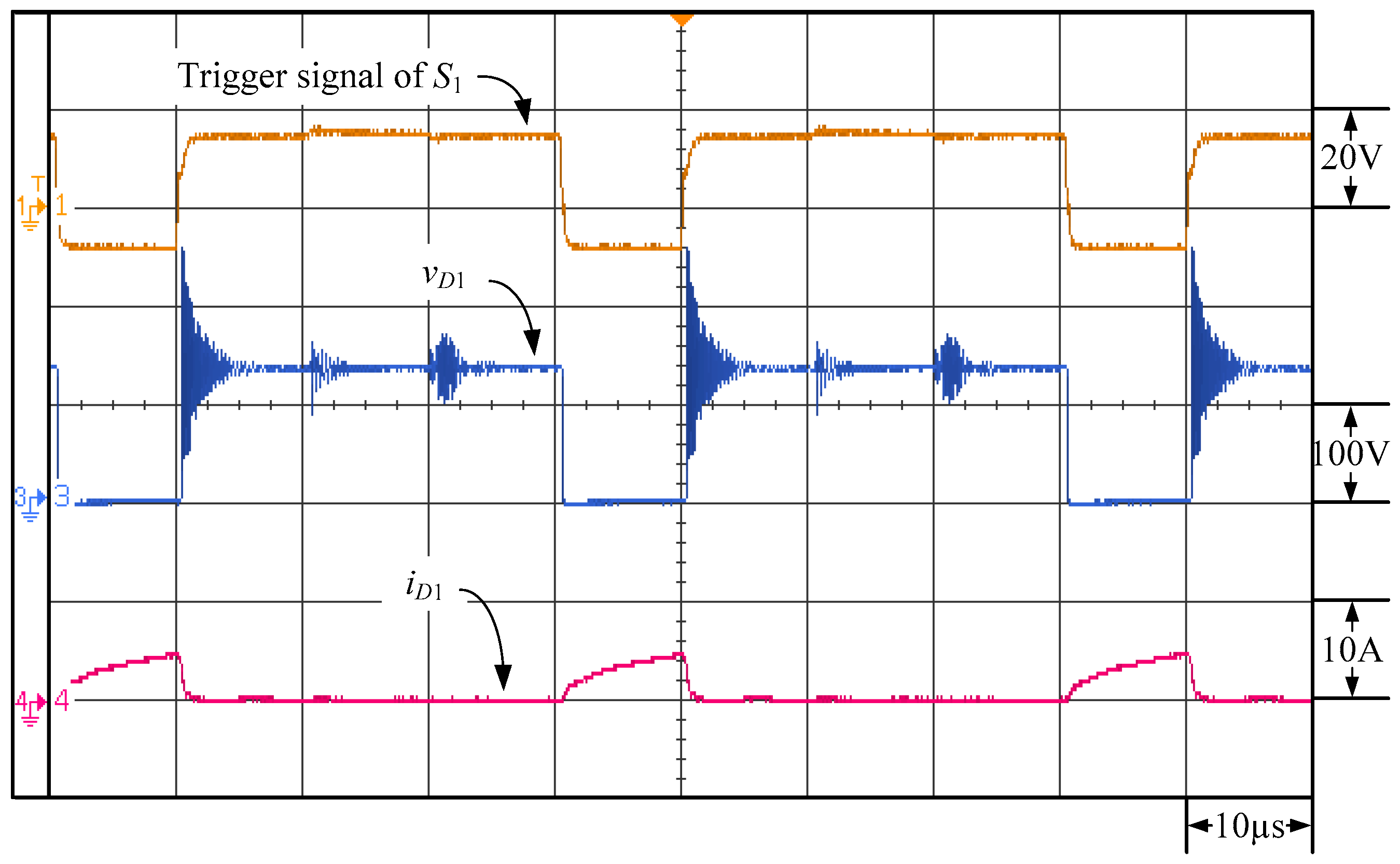
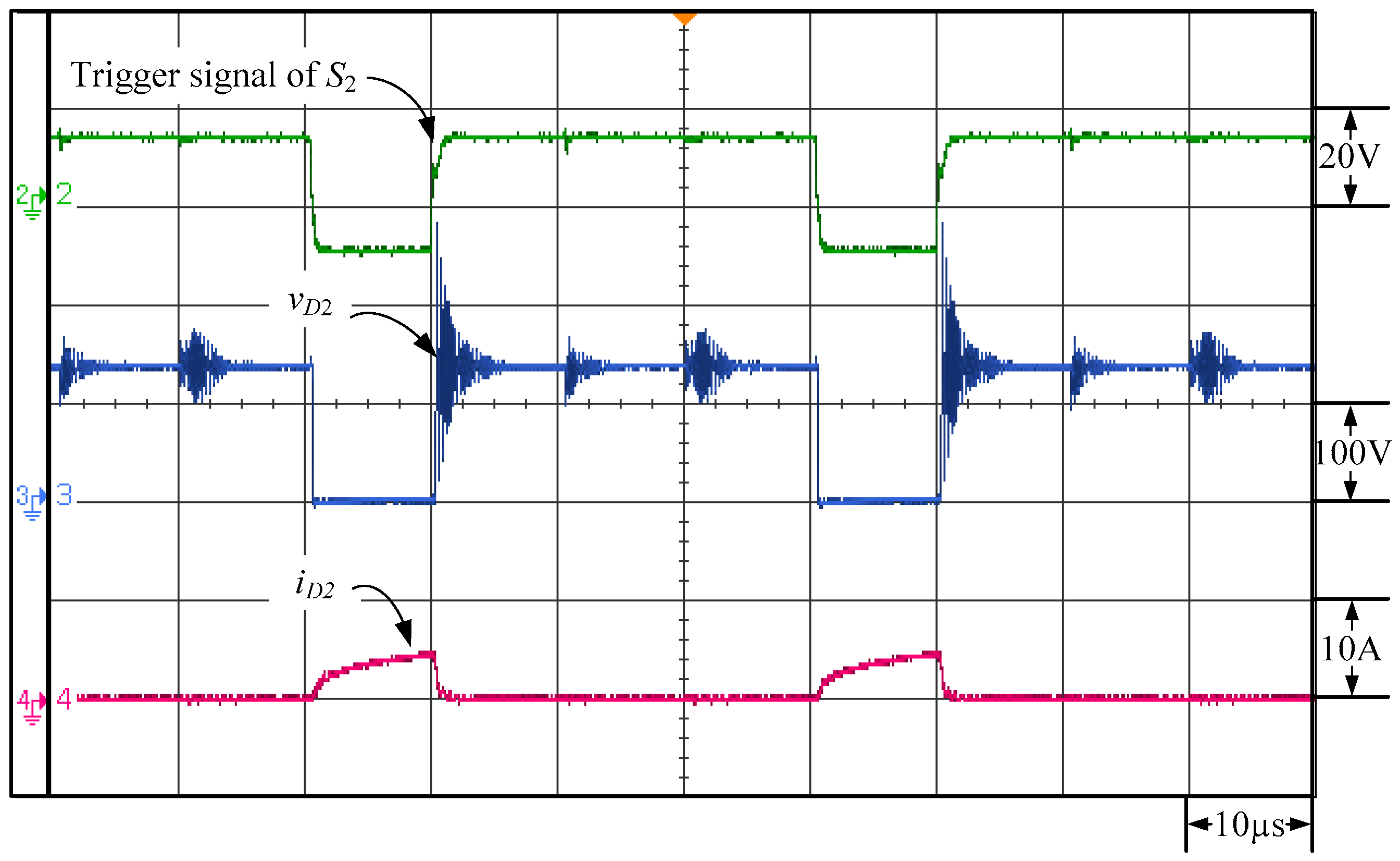
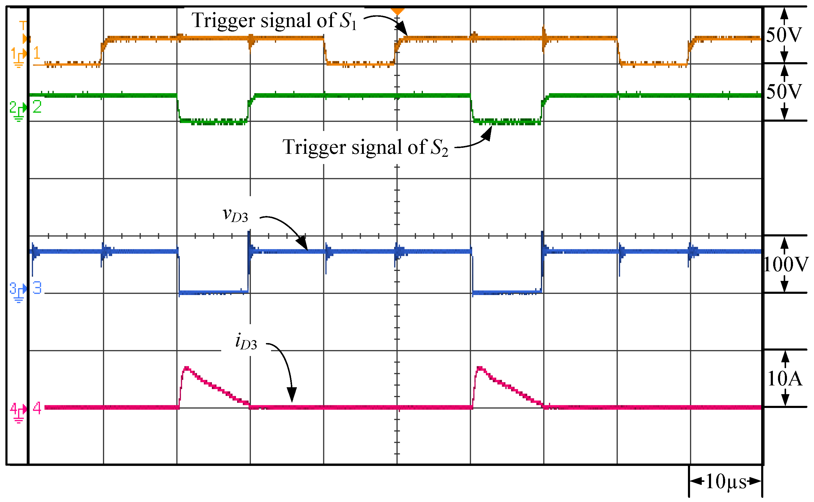
8. Experimental Results

This section is devoted to the experimental validation of PSIM simulations on a DC/DC converter with the electrical specifications listed in Table 5. A photo of the realized converter is presented in Figure 19, and Figure 20 illustrates the measured output voltage and current waveforms at an output power of 1000 W. With an extremely low level of ripples in the input and output current ii and io, the converter was found to be able to boost an input voltage of 18 V to an output voltage of 350 V. For comparison purposes, the waveforms measured at Po = 350 W are presented in Figure 21. As expected, a good performance agreement is seen once more between the simulation and experimental results. Figure 22 and Figure 23 illustrate the measured waveforms of the trigger signals for the main switches S1 and S2, the currents ids1 and ids2, and the voltage drops vds1 and vds2. As before, there is a good agreement between the simulation and experimental results, and the converter configuration meets the design requirement of components’ current/voltage ratings. Moreover, Figure 24 illustrates the measured current waveforms through the coupled inductors Lm1 and Lm2, where the ripple level of the input current ii is suppressed using an interleaving mechanism. Figure 25, Figure 26, Figure 27 and Figure 28 illustrate the measured current and voltage waveforms through and across the diodes D1D4. A good agreement is seen again between the simulation and experimental results.

9. Conclusions

This paper presents an interleaved inductor-coupled converter to boost the output voltage of fuel cells to a high voltage level and to overcome the problems of the voltage ratings of the involved power switches and diodes. By using the proposed circuit scheme of the converter, not only was the voltage gain increased, but the voltage ratings of power switches were also reduced. In addition, the current stress on the coupled inductors can be lowered, and the ripple level in the input current can be suppressed by using an interleaving mechanism. It is validated by simulation and experimental means to provide a high voltage conversion ratio, boosting an input voltage of 15 V to an output voltage of 350 V. In addition, as the output voltage is boosted, the voltage rating of power switches stays at Vi/(1 − D), meaning that it has no dependence on the output voltage, and the current rating is merely one half the input current. In conclusion, this paper presents a DC/DC converter with low cost but high performance due to a smaller number of required components, a high voltage conversion ratio, and low voltage and current stress on power switches.

Acknowledgments

This paper was sponsored by the Ministry of Science and Technology, Taiwan, under Grant No. MOST 104-2623-E-167-002-ET, and the authors feel deeply indebted to the Green Energy and Environment Research Laboratories, Industrial Technical Research Institute of Taiwan, for all the technical support.

Author Contributions

The mode analysis on the proposed interleaved inductor-coupled converter was made by Long-Yi Chang. Jung-Hao Chang carried out the simulations and experiments of the proposed converter. Kuei-Hsiang Chao was responsible for writing the paper and serves as the corresponding author. Kuei-Hsiang Chao also completed the components design of the proposed converter. Yi-Nung Chung measures the dynamic and steady-state performance of the proposed converter.

Conflicts of Interest

The authors declare no conflict of interest.

References

  1. Chen, Y.S.; Lin, S.M.; Hong, B.S. Experimental study on a passive fuel cell/battery hybrid power system. Energies 2013, 6, 6413–6422. [Google Scholar] [CrossRef]
  2. Hsieh, Y.P.; Chen, J.F.; Liang, T.J.; Yang, L.S. A novel high step-up DC-DC converter for a microgrid system. IEEE Trans. Power Electron. 2011, 26, 1127–1136. [Google Scholar] [CrossRef]
  3. Hsieh, Y.P.; Chen, J.F.; Liang, T.J.; Yang, L.S. Novel high step-up DC-DC converter for fuel cell energy conversion system. IEEE Trans. Ind. Electron. 2010, 57, 2007–2017. [Google Scholar]
  4. Prudente, M.; Pfitscher, L.L.; Emmendoerfer, G.; Romaneli, E.F.; Gules, R. Voltage multiplier cells applied to non-isolated DC-DC converters. IEEE Trans. Ind. Electron. 2008, 23, 871–887. [Google Scholar] [CrossRef]
  5. Pan, C.T.; Lai, C.M. A high-efficiency high step-up converter with low switch voltage stress for fuel cell system applications. IEEE Trans. Ind. Electron. 2010, 57, 1998–2006. [Google Scholar]
  6. Jung, D.Y.; Ji, Y.H.; Park, S.H.; Jung, Y.C.; Won, C.Y. Interleaved soft-switching boost converter for photovoltaic power-generation system. IEEE Trans. Power Electron. 2011, 26, 1137–1145. [Google Scholar] [CrossRef]
  7. Grötsch, M.; Mangold, M.; Kienle, A. Analysis of the coupling behavior of PEM fuel cells and DC-DC converters. Energies 2009, 2, 71–96. [Google Scholar] [CrossRef]
  8. Walker, G.R.; Sernia, P.C. Cascaded DC-DC converter connection of photovoltaic modules. IEEE Trans. Ind. Electron. 2004, 19, 1130–1139. [Google Scholar] [CrossRef]
  9. Alam, M.K.; Khan, F.H. Reliability analysis and performance degradation of a boost converter. IEEE Trans. Ind. Appl. 2014, 55, 3986–3994. [Google Scholar] [CrossRef]
  10. Hwang, T.S.; Park, S.Y. Seamless boost converter control under the critical boundary condition for a fuel cell power conditioning system. IEEE Trans. Power Electron. 2012, 27, 3616–3626. [Google Scholar] [CrossRef]
  11. Tseng, K.C.; Liang, T.J. Novel high-efficiency step-up converter. IEEE Trans. Power Electron. 2004, 151, 182–190. [Google Scholar] [CrossRef]
  12. Keum, M.H.; Choi, Y.; Han, S.K. High efficiency voltage-clamped coupled-inductor boost converter. In Proceedings of the 39th Annual Conference of the IEEE Industrial Electronics Society, Vienna, Austria, 10–13 November 2013; pp. 828–833.
  13. Lin, B.R.; Dong, J.Y. New zero-voltage switching DC-DC converter for renewable energy conversion systems. IET Power Electron. 2012, 5, 393–400. [Google Scholar] [CrossRef]
  14. Coruh, N.; Urgun, S.; Erfidan, T.; Ozturk, S. A simple and efficient implementation of interleaved boost converter. In Proceedings of the IEEE International Conference on Industrial Electronics and Applications, Beijing, China, 21–23 June 2011; pp. 2364–2368.
  15. Devi, M.A.; Valarmathi, K.; Mahendran, R. Ripple current reduction in interleaved boost converter by using advanced PWM techniques. In Proceedings of the IEEE International Conference on Advanced Communication Control and Computing Technologies, Ramanathapuram, India, 8–10 May 2014; pp. 115–119.
  16. Roh, Y.S.; Moon, Y.J.; Park, J.; Yoo, C. A two-phase interleaved power factor correction boost converter with a variation-tolerant phase shifting technique. IEEE Trans. Power Electron. 2014, 29, 1023–1040. [Google Scholar]
  17. Kosai, H.; McNeal, S.; Jordan, B.; Scofield, J.; Ray, B.; Turgut, Z. Coupled Inductor characterization for a high performance interleaved boost converter. IEEE Trans. Magn. 2009, 45, 4812–4815. [Google Scholar] [CrossRef]
  18. Jang, Y.T.; Jovanovic, M.M. Interleaved boost converter with intrinsic voltage-doubler characteristic for universal-line PFC front end. IEEE Trans. Power Electron. 2007, 22, 1394–1401. [Google Scholar] [CrossRef]
  19. Pan, C.T.; Lai, C.M.; Cheng, M.C.; Hsu, L.T. A low switch voltage stress interleaved boost converter for power factor correction. In Proceedings of the International Conference on Power Electronics and Drive Systems, Taipei, Taiwan, 2–5 November 2009; pp. 49–54.
  20. Lai, C.M.; Lin, Y.C.; Lee, D.S. Study and implementation of a two-phase interleaved bidirectional DC/DC converter for vehicle and DC-microgrid systems. Energies 2015, 8, 9969–9991. [Google Scholar] [CrossRef]
  21. Chang, L.Y.; Chao, K.H.; Chang, T.C. Application of high voltage ratio and low ripple interleaved DC-DC converter for a fuel cell. Sci. World J. 2012, 2012, 896508. [Google Scholar] [CrossRef] [PubMed]
  22. Pan, C.T.; Chuang, C.F.; Chu, C.C. A novel transformer-less adaptable voltage quadrupler DC converter with low switch voltage stress. IEEE Trans. Power Electron. 2014, 29, 4787–4796. [Google Scholar] [CrossRef]
  23. Lai, C.M.; Pan, C.T.; Cheng, M.C. High-efficiency modular high step-up interleaved boost converter for DC-microgrid applications. IEEE Trans. Power Electron. 2012, 48, 161–171. [Google Scholar] [CrossRef]
  24. Nguyen, T.V.; Petit, P.; Aillerie, M.; Salame, C.; Charles, J.P. Efficiency of magnetic coupled boost DC-DC converters mainly dedicated to renewable energy systems: Influence of the coupling factor. Int. J. Circuit Theory Appl. 2014, 43, 1042–1062. [Google Scholar] [CrossRef]
  25. Chen, Y.T.; Lin, W.C.; Liang, R.H. An interleaved high step-up DC-DC converter with double boost paths. Int. J. Circuit Theory Appl. 2014, 43, 967–983. [Google Scholar] [CrossRef]
  26. Horizon Fuel Cell Technologies. H-500XP Fuel Cell Stacks. Available online: http://www.horizoneducational.com/wp-content/uploads/2015/10/H-500XP_Stacks_Brochure_EN_v4_2015-10-12.pdf (accessed on 12 March 2016).
Figure 1. Configuration of the presented interleaved inductor-coupled boost converter.
Energies 09 00792 g001
Figure 2. Respective waveforms of the current through and the voltage across the components in the converter in Figure 1.
Energies 09 00792 g002
Figure 3. Equivalent circuit in Mode 1.
Energies 09 00792 g003
Figure 4. Equivalent circuit in Mode 2.
Energies 09 00792 g004
Figure 5. Equivalent circuit in Mode 3.
Energies 09 00792 g005
Figure 6. Equivalent circuit in Mode 4.
Energies 09 00792 g006
Figure 7. A family of voltage gain-duty cycle curves with N as a parameter.
Energies 09 00792 g007
Figure 8. Switch control signals and the current waveforms through the output capacitors over an operating cycle (t0t4).
Energies 09 00792 g008
Figure 9. Circuit configuration for power simulation (PSIM) software simulations.
Energies 09 00792 g009
Figure 10. Simulated input and output voltage/currents at an input voltage of 15 V, an output voltage of 350 V, and an output power of 1000 W.
Energies 09 00792 g010
Figure 11. Simulated waveforms related to the power switch S1.
Energies 09 00792 g011
Figure 12. Simulated waveforms related to the power switch S2.
Energies 09 00792 g012
Figure 13. Simulated current waveforms through the coupled inductors Lm1 and Lm2.
Energies 09 00792 g013
Figure 14. Simulated voltage and current waveforms for the diode D1.
Energies 09 00792 g014
Figure 15. Simulated voltage and current waveforms for the diode D2.
Energies 09 00792 g015
Figure 16. Simulated voltage and current waveforms for the diode D3.
Energies 09 00792 g016
Figure 17. Simulated voltage and current waveforms for the diode D4.
Energies 09 00792 g017
Figure 18. Simulated waveforms for the output capacitor current iCo1iCo3.
Energies 09 00792 g018
Figure 19. A photo of the realized interleaved inductor-coupled boost converter.
Energies 09 00792 g019
Figure 20. Measured voltage and current waveforms in the input and output at an output power of 1000 W for the implemented boost converter.
Energies 09 00792 g020
Figure 21. Measured voltage and current waveforms in the input and output at an output power of 350 W for the implemented boost converter.
Energies 09 00792 g021
Figure 22. Measured waveforms related to the power switch S1.
Energies 09 00792 g022
Figure 23. Measured waveforms related to the power switch S2.
Energies 09 00792 g023
Figure 24. Measured current waveforms through the coupled inductors Lm1 and Lm2.
Energies 09 00792 g024
Figure 25. Measured voltage and current waveforms for the diode D1.
Energies 09 00792 g025
Figure 26. Measured voltage and current waveforms for the diode D2.
Energies 09 00792 g026
Figure 27. Measured voltage and current waveforms for the diode D3.
Energies 09 00792 g027
Figure 28. Measured voltage and current waveforms for the diode D4.
Energies 09 00792 g028
Table 1. Specifications of a Horizon (H-500XP) proton exchange membrane (PEM) fuel.
ParameterSpecifications
Number of Cells30
Rated Power500 W
Rated Performance18 [email protected] A
Operating Voltage Range15–30 V
External Temperature0–35 °C
ReactantsHydrogen and Air
Max Stack Temperature63 °C
Hydrogen Pressure7.2–9.4 PSI
Hydrogen Flow Rate at Max Output5.86 L/min
Stack Size130 × 203 × 52 mm
Weight3.9 kg
Hydrogen Purity Requirement99.99% dry Hydrogen
Table 2. The expected good design performance of the proposed boost converter with coupled inductor.
Voltage GainVoltage Rating of SwitchesCurrent Rating of SwitchesVoltage Rating of DiodesNumber of InductorsNumber of CapacitorsNumber of Diodes
Vo/ViVds1, Vds2Ids1Ids2
2 V o V i V 0 2 I i 2 I i V o 2 4 4
Table 3. Performance and requirement comparison among representative types of boost converters and this proposal.
ConvertersVoltage GainVoltage Rating of Switches Vds1, Vds2Current Rating of SwitchesVoltage Rating of DiodesNumber of InductorsNumber of CapacitorsNumber of Diodes
Vo/ViIds1Ids2
Converter in [4] 3 1 D V o 3 I i I i 2 V o 3 234
Converter in [17] 1 1 D V o I i 2 I i 2 V o 212
Converter in [19] 2 1 D V o 2 I i 2 I i V o 222
Converter in [22] 2 1 D V o 2 I i I i V o 222
Converter in [23] 2 1 D + N D V o 2 + N D ( 1 D ) I i 2 I i 2 V o 2 + N D ( 1 D ) 334
Converter in [24] 1 + N D 1 D V o + N V i 1 + N ( 1 + N ) I i V o + N V i 111
Converter in [25] 3 1 D V o 3 I i I i 2 V o 3 233
Proposed converter 2 N D + 2 1 D V o 2 N D + 2 I i 2 I i N V o 2 N D + 2 244
Table 4. Design parameters and settings for the presented boost converter.
ParameterSpecifications
Range of input voltage range (Vin)15–30 V
Output voltage (Vo)350 V
Power rating (Po)1000 W
Switching frequency (f)25 kHz
Table 5. Electrical specifications and component model numbers involved in the implemented boost converter.
ParameterSpecification
Range of input voltage range (Vi)Vi = 15–30 V
Output voltage (Vo)Vo = 350 V
Switching frequency (f)f = 25 kHz
Power rating (Po)Po = 1000 W
Coupled inductance (Lm1, Lm2)Lm1 = Lm2 = Lm = 35 µH
Turns ratio of coupled inductor (N)N = 2
Clamped capacitance (C1)C1 = 470 µF
Power switches (S1, S2)MMG100J030U (600 V/100 A)
Diodes (D1, D2, D3, D4)IQBD30E60A1 (600 V/60 A)
Output capacitance (Co1, Co2, Co3)Co1= Co2 = Co3 = 470 µF

