Article

Smooth Switching Technique for Voltage Balance Management Based on Three-Level Neutral Point Clamped Cascaded Rectifier

School of Electrical Engineering, Southwest Jiaotong University, Chengdu 610031, China
*
Author to whom correspondence should be addressed.
Energies 2016, 9(10), 803; https://doi.org/10.3390/en9100803
Submission received: 15 April 2016 / Accepted: 26 September 2016 / Published: 3 October 2016
(This article belongs to the Special Issue Power Electronics Optimal Design and Control)

Abstract

:
This paper discussed the topology of in the three-level neutral point clamped cascaded rectifier (3LNPC-CR) for designing the Chinese Power Electronic Traction Transformer (PETT). To balance the DC-link voltage (Vdc) in 3LNPC-CR, a smooth switching technique is proposed in this paper. The controlling processes of each module are relatively independent when the proposed technique is applied in 3LNPC-CR. The proposed technique can keep the switching frequency constant and change the switch state smoothly while balancing Vdc. The Vdc balance ability is analyzed by calculating the unbalance degree of the loads. Simulation and experiment of three-module 3LNPC-CR are built, and then the effectiveness of the proposed technique is verified.

1. Introduction

In the past decade, various multilevel converter topologies, including the three-level neutral point clamped converter (3LNPC), modular multilevel converter (MMC) and cascaded H-bridge (CHB), are widely used in the industry [1,2]. To apply them in high voltage and high power situations, the modulations of the converters become complicated when the output voltage of the multilevel converter increases [3,4]. Among multilevel converter topologies, the CHB is used as a rectifier because it could convert the high AC voltage to the low DC voltage [5,6]. Thus, the cascaded H-bridge rectifier (CHBR) is used in the Solid-State Transformer (SST) to achieve the Internet of Energy in the smart grid [5]. In the SST, CHBR transforms the grid voltage to the lower DC-link voltage of each module. Moreover, CHBR is also applied in the Power Electronic Traction Transformer (PETT) for the 15 kV single phase voltage traction system in Europe [6]. PETT, with the similar topology to that of SST, could replace the traction transformer to step-down the voltage on the locomotive. PETT could save the weight and volume for the locomotive. Since Chinese traction system uses 25 kV single phase voltage, the voltage level of each module should increase. In [7], CHB with 3LNPC module is used in the Advanced Traction Power Supply System (ATPSS), when facing the 25 kV traction system single phase voltage. The ATPSS is used to solve the power quality problems of the traditional traction power supply system, such as unbalance, reactive power and harmonics to three-phase industrial grid. Thus, PETT of China has the possibility to design CHBR with 3LNPC module, as the Three-Level Neutral Point Clamped Cascaded Rectifier (3LNPC-CR) shown in Figure 1a. Moreover, A Hani Packed U-cell (HPUC) is proposed for regulating dual DC-link voltage [8,9]. Although CHB and HPUC are compact and easy to implement, 3LNPC has shown its ability to deal with the high voltage in the traction power supply system [7,8,9]. Zou et al. [10] introduced a control strategy for the single phase rectifier, which is widely used in the railway application.
The 3LNPC suffers from fluctuation of the neutral point voltage [11,12,13,14,15]. Kinds of auxiliary balance circuits have been proposed to solve this fluctuation [11,12]. Shu et al. [11] proposed an inductor-based auxiliary circuit for the multilevel converter, while Zhu et al. [12] proposed a capacitor-based one. The auxiliary circuits are efficient in achieving the voltage balance, but they also give rise to additional hardware cost. An algorithm using logical comparison for selecting the redundant switch state was applied in [13], which could balance the neutral point voltage. Another balancing strategy to solve the fluctuation is to adjust the duty time of the redundant vector [14]. This method has also been applied to a single-phase multilevel converter [15].
Apart from the fluctuation of the neutral point voltage, the cascaded converter suffers from DC-link voltage unbalance caused by inconsistency in the loads of each module [16,17,18,19,20,21,22]. The PETT paralleled the output of the DC/DC converter, so that each module has to be rated at full power [16]. Thus, there is no unbalance the load in CHBR. In [17,18], the modulation waves are adjusted by proportional-integral (PI) controller for balancing the voltage. A switching technique has been proposed and applied to improve DC-link voltage (Vdc) balance performance of CHBR for extending the voltage balance region [19,20,21,22]. Due to the equivalence of each module in CHBR, the technique can exchange the switch states of each module to balance the Vdc. These switching techniques are more effective compared with PI-based voltage balancing method [19]. The implementation of the switching technique consists of region judgment, rank and switch states exchanging [20]. Firstly, two regions are divided according to whether the grid current (is) is positive. Secondly, the modules are ranked by their Vdc and the switch states are ranked by their synthesize voltage. In one H-bridge module, three switch states, namely 1 (Vdc), 0 (0) and −1 (−Vdc), are categorized. The module can absorb power on 1 and release power on −1 when is is positive. On the contrary, the module can absorb power on −1 and release power on 1 when is is negative. Especially, 0 rejects power no matter what is is. Lastly, the criterion of switch states exchanging is shown as follows: the module with higher Vdc acquires the switch state releasing or rejecting power from the grid; the module with lower Vdc acquires the switch state to absorb or reject power from grid. In [20], the CHBR can balance Vdc of each module when the load of one module is removed. However, switch state of module will jump from 1 to −1 when the switching technique is working. This jump enlarges the switch frequency of the power device. A 3-D space modulation has been proposed in 3-module CHBR to solve the jumping problem [21]. The 3-D space modulation describes the switch state of each module in a three-module CHBR as the three dimensions of the space, then, the switch moves smoothly in this space. The 3-D space modulation could not be directly used in 3LNPC-CR due to increased kinds of the switch states. Moreover, it is not convenient to extend the 3-D space modulation to n-D when the number of the module grows to n (n > 3). In terms of the voltage balance calculation, Vazquez et al. [22] found the limitation of voltage balance ability in two-module converter and concisely illustrated the limitation by the voltage vector.
The topology of 3LNPC-CR is discussed in this paper for designing the Chinese PETT. To balance the Vdc in 3LNPC-CR, a smooth switching technique is proposed. The proposed switching technique maintains the switching frequency and keeps the switch states changing smoothly in this paper. The paper is organized as follows: Section 2 describes the configuration of the 3LNPC-CR and the neutral point voltage fluctuation control of 3LNPC; Section 3 shows the proposed smooth switching technique; Section 4 calculates the voltage balance ability of 3LNPC-CR; and Section 5 verified the theory of this paper by simulation and experiment.

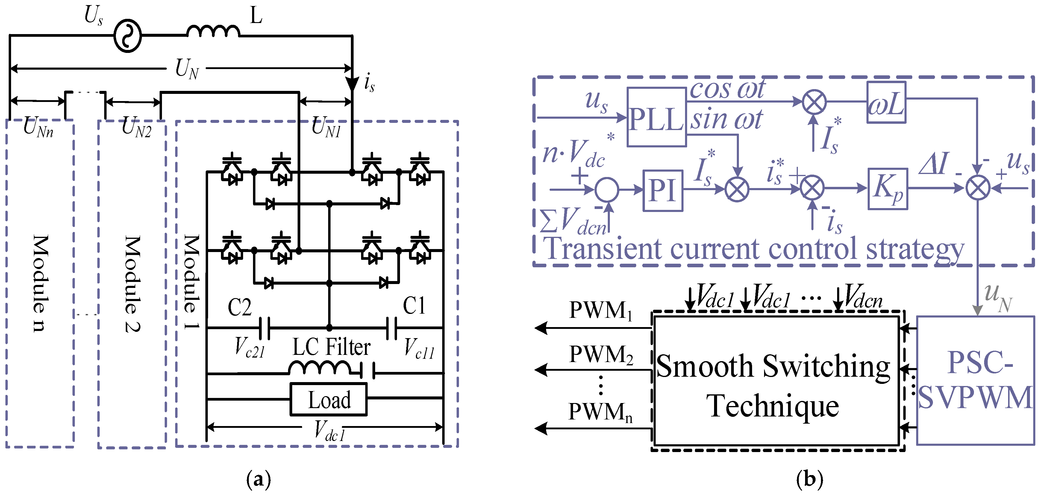
2. Configuration and Control of Three-Level Neutral Point Clamped Cascaded Rectifier

2.1. Configuration and Control of Three-Level Neutral Point Clamped Cascaded Rectifier

3LNPC-CR is illustrated in Figure 1a, which is made up of 3LNPC module. One 3LNPC module is made up of the 3LNPC converter, which used to synthesize output voltage, and the LC filter, which filters the DC voltage fluctuations. All 3LNPC modules are cascaded to face the higher grid voltage. L is the inductor of the single phase rectifier. Figure 1b shows control system of 3LNPC-CR: The transient current control strategy (TCCS) is applied for the single phase rectifier [10]. Once the result of TCCS (uN) is acquired, it will be modulated by the phase shift carrier space vector pulse width modulation (PSC-SVPWM), which generates the standard pulse width modulation (PWM) signals for the 3LNPC-CR. However, the PWM signals generated by PSC-SVPWM have no voltage balance ability when the loads of 3LNPC-CR are unbalanced. After PSC-SVPWM modulation, all the PWM signals generated by PSC-SVPWM are rearranged by the smooth switching technique, and the rearranged PWM signals will be used as the switch state (PWM1 to PWMn), which could balance the DC-link voltage with unbalance the load. The smooth switching technique rearranged the switch state by judging the sum of the switch state, the value of DC-link voltage and the direction of grid current. Additionally, after the rearrangement by the smooth switching technique, the sum of switch state remains unchanged compared with the sum of switch state generated by PSC-SVPWM. The detail process of the rearrangement is illustrated in Section 3.3.
Figure 1b shows the control system of 3LNPC-CR. The transient current control is applied to the single phase rectifier [10]. According to the mathematical model of the single phase 3LNPC rectifier, the output voltage uN in Figure 1b could be expressed by TCCS according to [10]:
{ u N ( t ) = u s ( t ) ω L s I s * cos ω t K p ( I s * sin ω t i s ( t ) ) I s * = K p ( n V d c * V d c n ) + 1 / T i ( n V d c * V d c n ) d t Δ I = K p ( I s * × sin ω t i s ( t ) )
where n is the number of 3LNPC modules. Phase locked loop (PLL) is a detective procedure that is used to acquire the phase of the grid voltage. Vdcn is the DC-link capacitors voltage value of the n-th module. Vdc* is the reference DC-link capacitors voltage of one single 3LNPC module. Is* is a reference current value given by a PI controller, which is used to maintain the DC-link voltage as the outer voltage loop. Kp and Ti are both the parameters of the PI controller. According to Figure 1a, uS(t) is the instantaneous voltage of the AC voltage source, iS(t) is the instantaneous current through each 3LNPC module, and uN(t) is the instantaneous terminal voltage of all modules. ΔI is the inner current loop, which is used to keep is sinusoidal.

2.2. Neutral Point Voltage Fluctuation Control of 3LNPC

According to the output voltage of 3LNPC, five categories of PWM from nine kinds of switch states are defined; i.e., 2 (Vdc), 1 (Vdc/2), 0 (0), −1 (−Vdc/2), and −2 (−Vdc). In this section, only four kinds of switch states are analyzed, as demonstrated by Figure 2. Figure 2a shows the switch state 00, which uses capacitor C1 to synthesize 0.5Vdc. Figure 2b shows the switch state 01, which uses capacitor C2 to synthesize 0.5Vdc. Figure 2c shows the switch state 10, which uses capacitor C1 to synthesize −0.5Vdc. Figure 2d shows the switch state 11, which uses capacitor C2 to synthesize −0.5Vdc. The 00 switch state and the 01 switch state represent the switch states, each acting as the redundant switch states of the other, which synthesized −0.5Vdc. These two switch states are called small positive (SP) switch states. The 10 switch state and the 11 switch state represent the switch states, each acting as the redundant switch states of the other, which synthesized −0.5Vdc. These two switch states are called small negative (SN) switch states. When is > 0, 00 (01) switch state makes 3LNPC charge C1 (C2), otherwise, 00 (01) switch state makes 3LNPC discharge C1 (C2). In terms of 10 and 11 switch states, when is > 0, 10 (11) switch state makes 3LNPC discharge C1 (C2), otherwise, 00 (01) switch state makes 3LNPC charge C1 (C2). When the four kinds of switch states need to be synthesized, the unequal charging (or discharging) between C1 and C2 will lead to the fluctuation of the neutral point voltage. Based on the analysis above, Table 1 summarizes the characteristic of these switch states.
The strategy for solving the fluctuation of the neutral point voltage is achieved by using different redundant switch states. The principle of the strategy is shown in Table 2. Based on the situation of the capacitor voltage and the grid current, there are four kinds of redundant switch state choices. However, on the premise of the principle, if the comparison result of Vc1 and Vc2 changes too frequently, the 3LNPC will suffer from the rise in switching frequency. The procedures of the fluctuation balance strategy for keeping the switching frequency normal are shown in Figure 3. In Figure 3, the procedure is able to select between 00 state and 01 state when none of them are working. Similarly, 10 state or 11 state could be selected when none of them are working. The result of the selection between 00 (10) and 01 (11) will be put into register which named sp(sn), and the state of the register is sent to synthesize the switch state (state) finally. When any one of 00 or 01 (10 or 11) switch state is working, sp(sn) remains unchanged. For instance, in Figure 3a, when 3LNPC-CR starts to work, every module must judge whether they should synthesize SP; that is, whether PWMx = 1 is judged all the time, where PWMx is the output voltage of module x. If PWMx = 1, the SP will remain unchanged and the module will synthesize SP. Otherwise, SP will choose between 00 and 01 based on the value of is, Vc1 and Vc2. Then, whether PWMx = 1 should be judged again, thus forming an endless loop.

3. Proposed Smooth Switching Technique

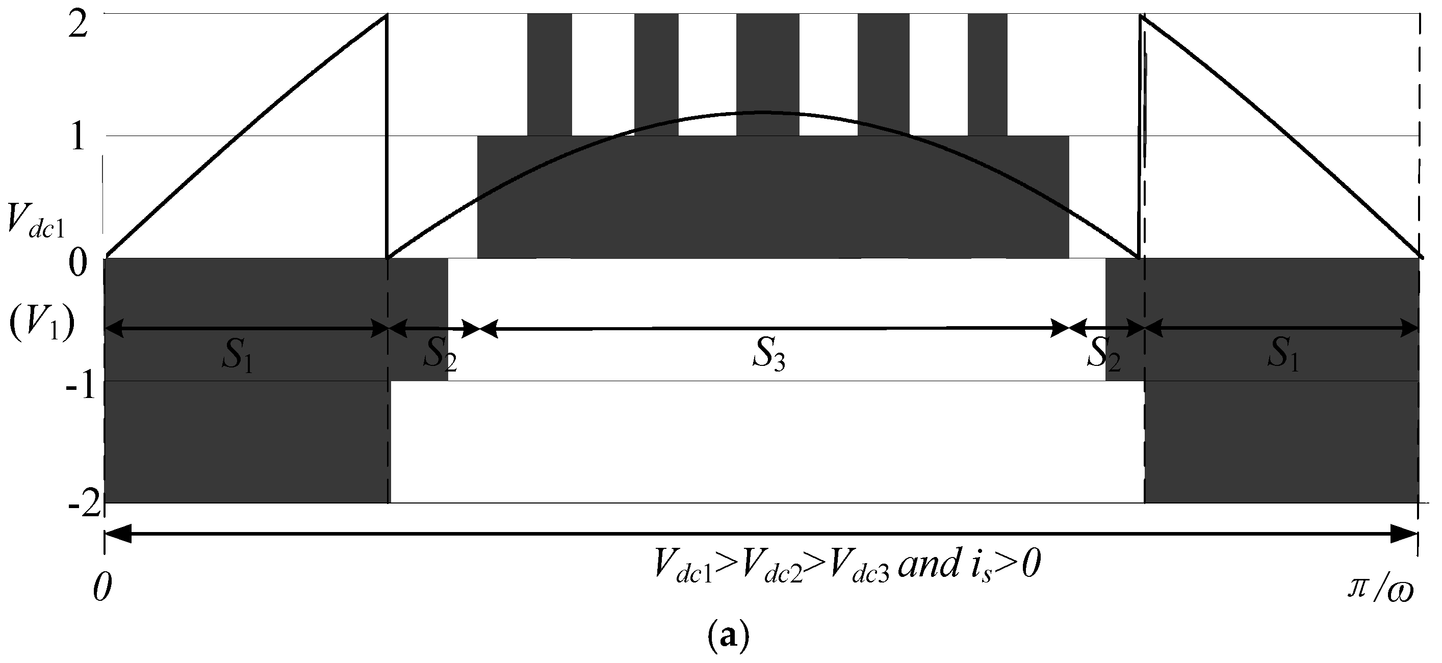
3.1. Analysis of the Voltage Balance

Vdcx is the result of Vc1x and Vc2x according to Figure 1a:
V d c x = V c 1 x + V c 2 x
where Vc1x and Vc2x are the voltages of capacitor C1 and C2 in 3LNPC module, respectively. Based on the power conservation of 3LNPC, the equation can be given as follow:
U N x i s = C 1 x V c 1 x d V c 1 x d t + C 2 x V c 2 x d V c 2 x d t + ( V c 1 x + V c 2 x ) 2 R x
where Rx is the load of module x, and UNx is the output voltage of module x, which is determined by the switch states. The is is same for all modules as 3LNPC-CR is a series circuit. Thus, when the different loads lead to the drift of Vdcx, the drift will be balanced by controlling switch states. Moreover, the module x could release its power when UNx and is are opposite.
The switch states of 3LNPC module are shown in Figure 4. There are 32 = 9 switch states in the 3LNPC, as shown in Figure 4a–i. Supposing that the voltage balancing strategy functions properly, the detailed instructions are illustrated as follows:
(a)
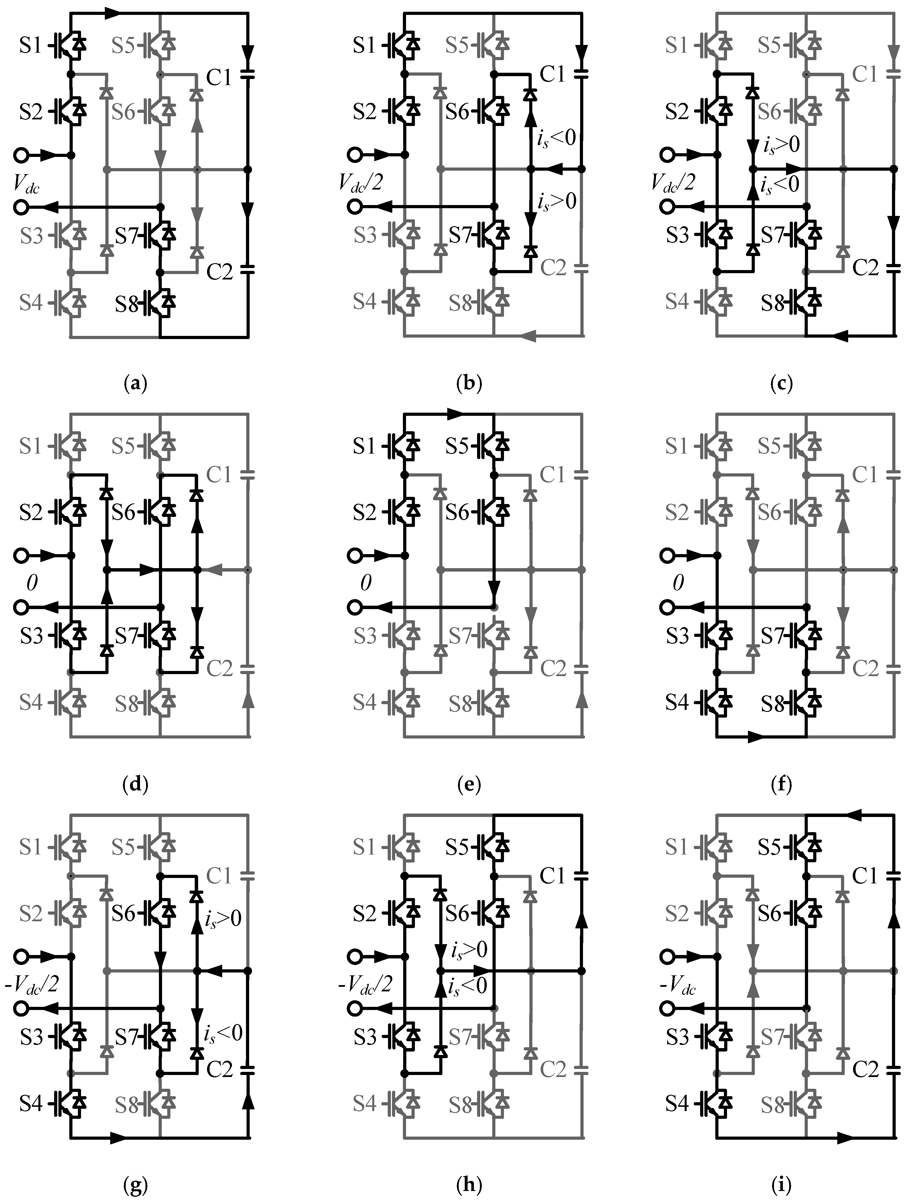
Switch State I: The switches S1, S2, S7 and S8 are on, while S3, S4, S5 and S6 are off. The output voltage is Vdc. C1 and C2 are charged when is > 0, and C1 and C2 are discharged when is < 0.
(b)
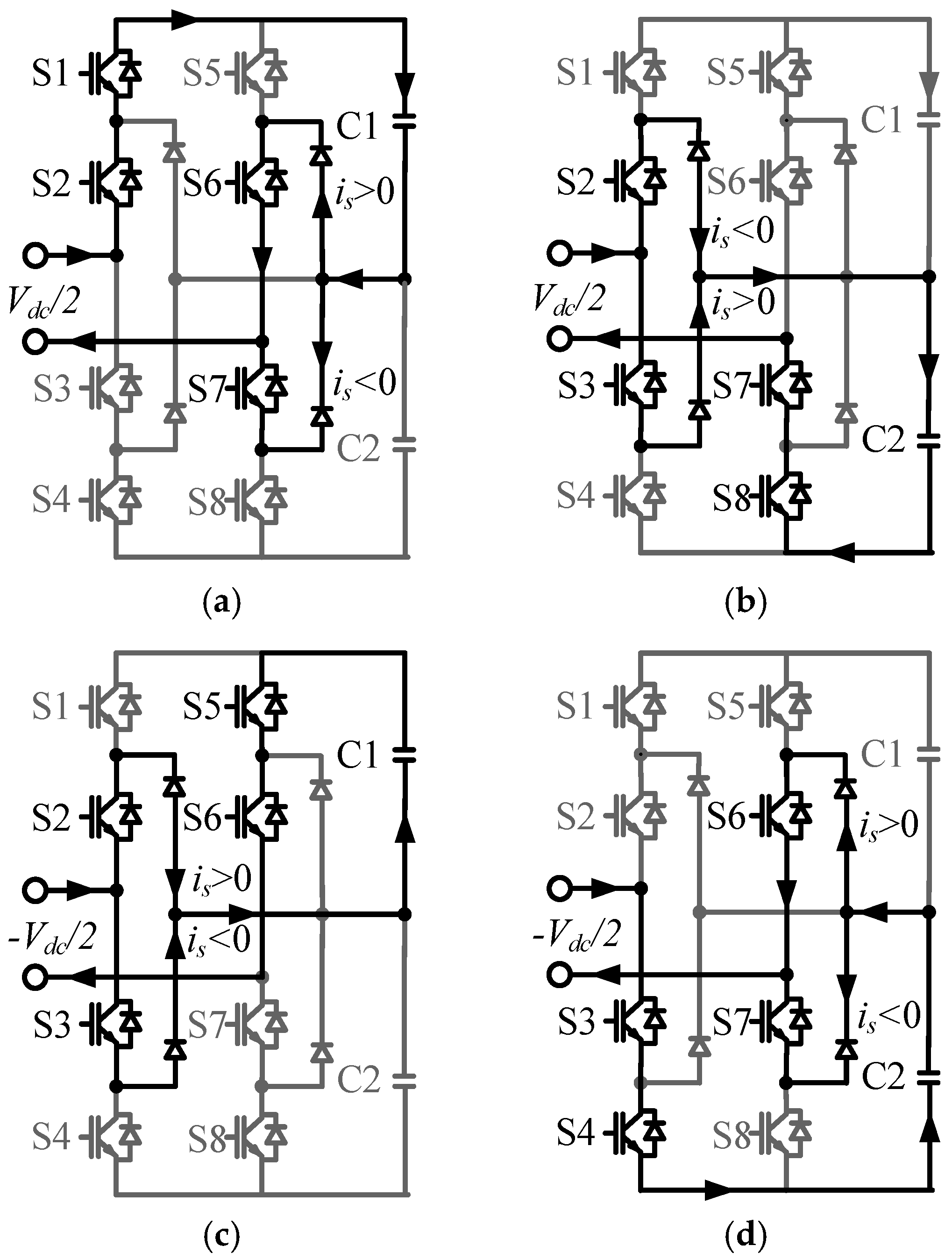
Switch State II: The switches S1, S2, S6 and S7 are on, while S3, S4, S5 and S8 are off. The output voltage is Vdc/2. C1 is charged when is > 0, and C1 is discharged when is < 0.
(c)
Switch State III: The switches S2, S3, S7 and S8 are on, while S1, S4, S5 and S6 are off. The output voltage is Vdc/2. C2 is charged in when is > 0, and C2 is discharged when is < 0.
(d)
Switch State IV: The switches S2, S3, S6 and S7 are on, while S1, S4, S5 and S8 are off. The output voltage is 0. The source has no effect on C1 or C2.
(e)
Switch State V: The switches S1, S2, S5 and S6 are on, while S3, S4, S7 and S8 are off. The output voltage is 0. The source has no effect on C1 or C2.
(f)
Switch State VI: The switches S3, S4, S7 and S8 are on, while S1, S2, S5 and S6 are off. The output voltage is 0. The source has no effect on C1 or C2.
(g)
Switch State VII: The switches S3, S4, S6 and S7 are on, while S1, S2, S5 and S8 are off. The output voltage is −Vdc/2. C2 is discharged when is > 0, and C2 is charged when is < 0.
(h)
Switch State VIII: The switches S2, S3, S5 and S6 are on, while S1, S4, S7 and S8 are off. The output voltage is −Vdc/2. C1 is discharged when is > 0, and C1 is charged when is < 0.
(i)
Switch State IX: The switches S3, S4, S5 and S6 are on, while S1, S2, S7 and S8 are off. The output voltage is −Vdc. C1 and C2 are charged reversely when is > 0, and C1 and C2 are when is > 0.
Obviously, the switch state of Figure 4a and the switch state of Figure 4i could adjust the DC-link voltage dramatically by charging or discharging the C1 and C2. Then come to the switch state of Figure 4b, the switch state of Figure 4c, the switch state of Figure 4g and the switch state of Figure 4h, they could change the DC-link voltage by charging or discharging the corresponding capacitor (C1 or C2). Although the switch state of Figure 4d, the switch state of Figure 4e and the switch state of Figure 4f have do not affect C1 or C2, these switch states could synthetize the voltage when needed.

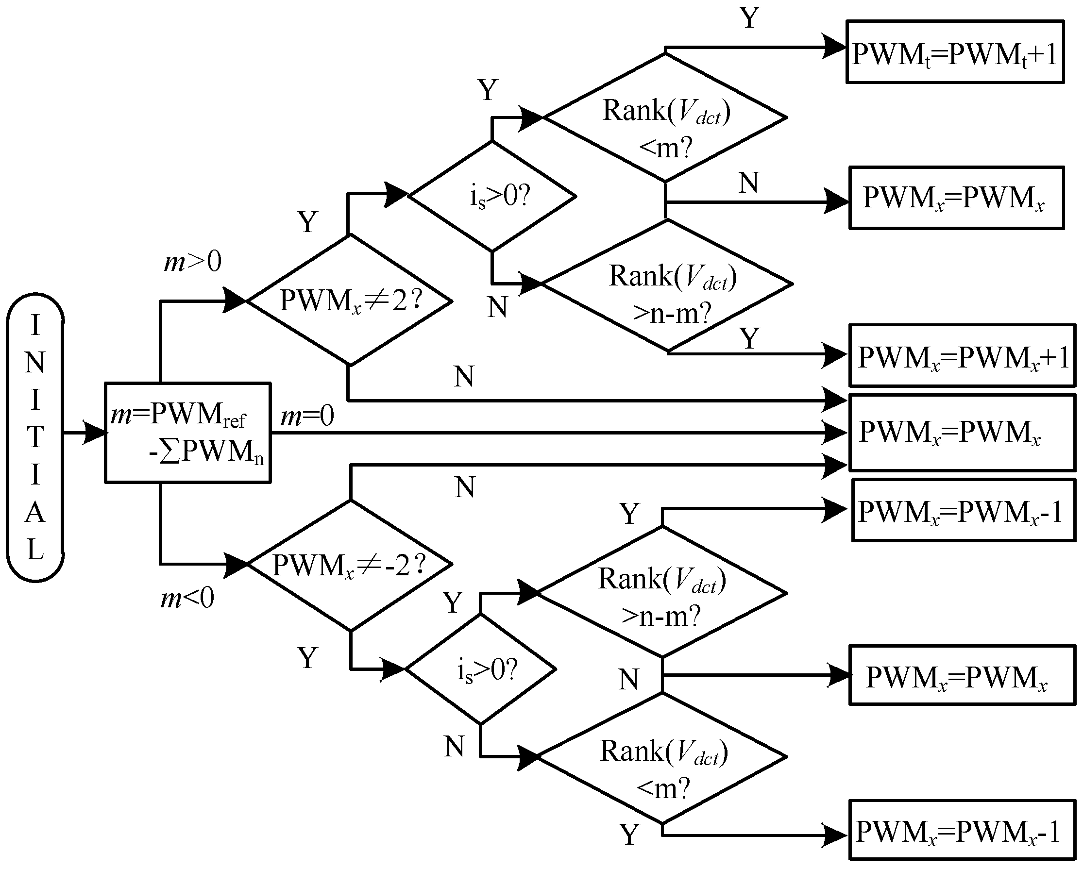
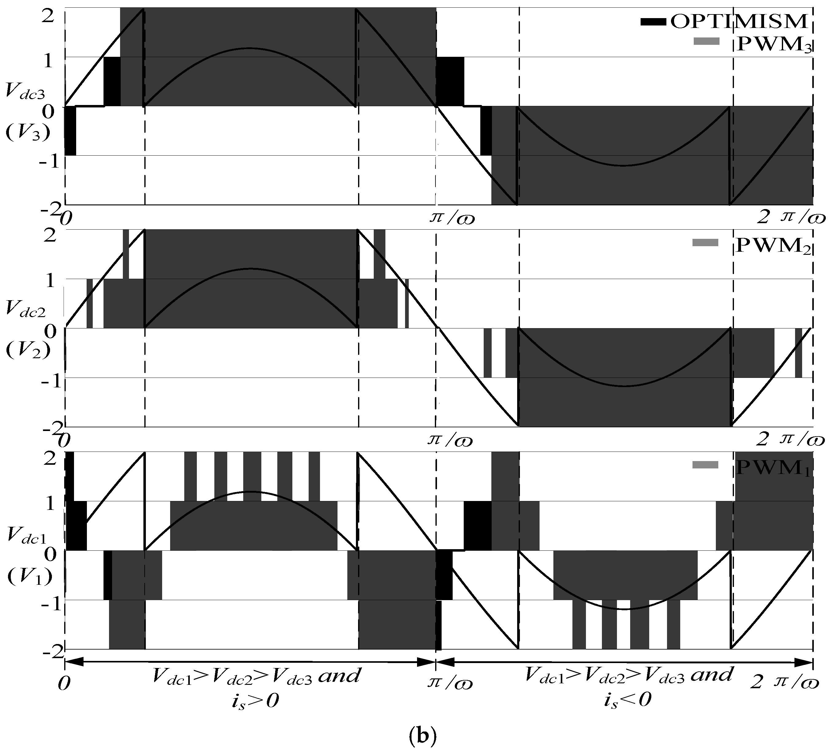
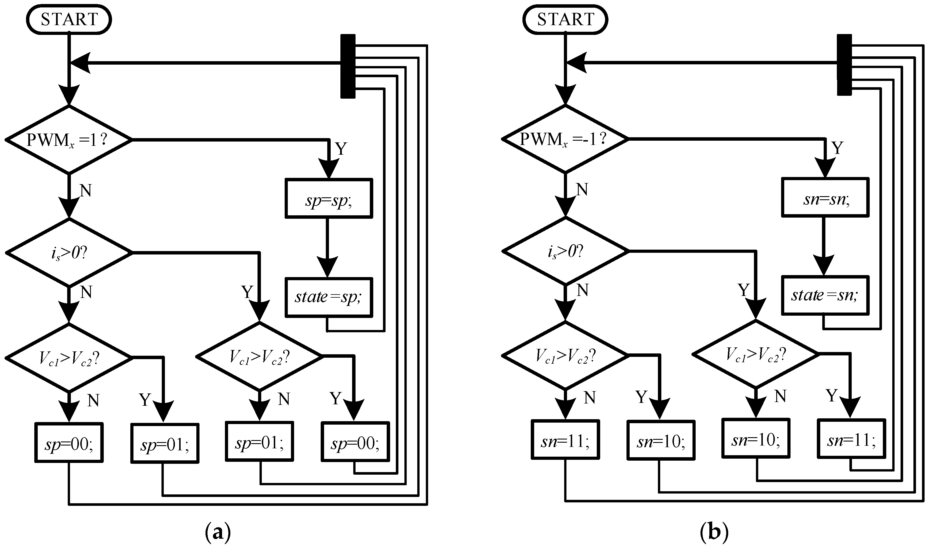
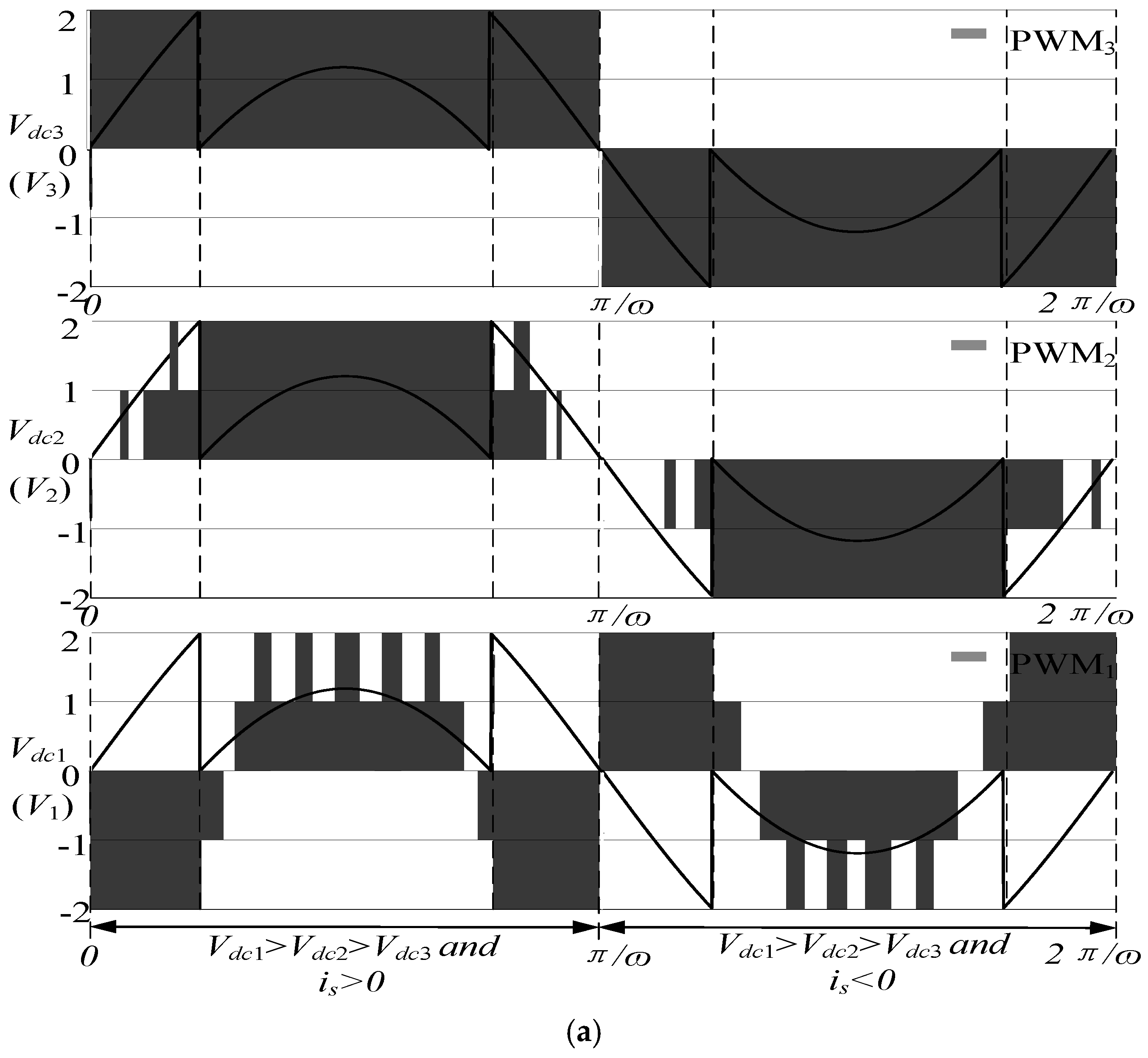
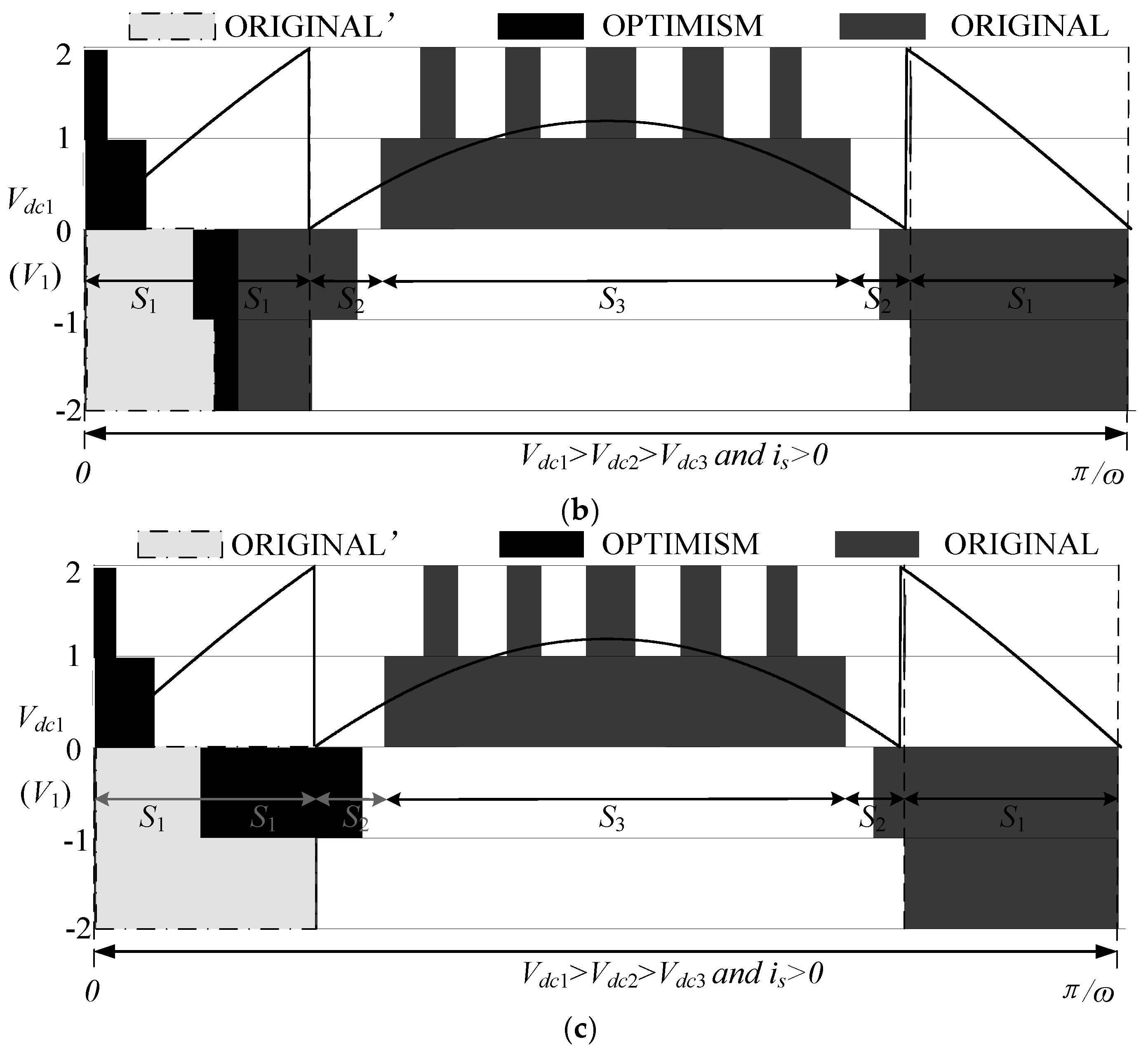
3.2. Switching Technique

Five categories of PWM are defined: 2 (Vdc), 1 (Vdc/2), 0 (0), −1 (−Vdc/2), and −2 (−Vdc). When the bias of the DC-link voltage among all modules is neglected, the voltage relationship can be built for illustrating the switching technique.
{ 2 a 2 b + P W M s = P W M r e f a + b + 1 = n P W M s [ 2 , 2 ]
where a is the number of modules whose PWM is 2, b is the number of modules whose PWM is −2, PWMs is a special PWM which could guarantee the synthesis of PWMref, n is the number of the module, and PWMref is the sum of reference PWM from module 1 to n. The more the 2 and −2 the converter has, the stronger voltage balance ability it will acquire. With the limitation above, a and b could be calculated as:
{ a = ( 2 n 2 + P W M s P W M r e f ) / 4 b = ( 2 n 2 + P W M s + P W M r e f ) / 4 P W M s [ 2 , 2 ]
Then, the DC-link voltages of all modules are ranked. Define the result of rank as (V1, V2, …, Vn), where (V1, V2, …, Vn) is the descending order for the DC-link voltage of all modules. According to the analysis of part B, the PWM of each module are arranged as in Table 3. When is > 0, the module which is of higher DC-link voltage requires lower PWM, and vice versa. In addition, when is < 0, the module which is of higher DC-link voltage requires higher PWM, and vice versa.

3.3. Smooth Switching Technique

The proposed technique is illustrated as Figure 5, which shows the rearrangement process in Section 2.1. The rank (Vdc1) is the function for ranking the DC-link voltage. The m is the difference between the sum of reference PWM from module 1 to n (PWMref) and the sum of PWM from module 1 to n. According to the output voltage, judged by the m and is, the voltage balance rules of module x are as follow:
When m = 0 whatever is is: it indicates that PWMref is equal to the sum of PWM from module 1 to n, that is, the PWM of all modules remains constant.
When m > 0 and is > 0: the sum of PWM from module 1 to n needs to plus m. Vdcx is the DC-link voltage of the module x. The PWM of module x could not increase any more when it is 2. Otherwise, the PWM of module x should plus 1 if the Vdcx is the smallest among 3LNPC-CR except for the module whose PWM is 2.
When m > 0 and is < 0: the sum of PWM from module 1 to n needs to plus m. The PWM of module x could not increase any more when its PWM is 2. Otherwise, the PWM of module x should plus 1 if the Vdcx is the biggest Vdc among 3LNPC-CR except for the module whose its PWM is 2.
When m < 0 and is > 0, the sum of PWM from module 1 to n needs to minus m. The PWM of module x could not decrease any more when its PWM is −2. Otherwise, the PWM of module t should minus 1 if the Vdcx is the biggest Vdc among 3LNPC-CR except for the module whose PWM is −2.
When m < 0 and is < 0, the sum of PWM from module 1 to n needs to minus m. The PWM of module x could not decrease any more when its PWM is −2. Otherwise, the PWM of module t should be minus 1 if the Vdcx is the m smallest Vdc among 3LNPC-CR except for the module whose PWM is −2.
The switching technique and the proposed smooth switching technique are illustrated in Figure 6, taking three-module single phase 3LNPC-CR as an example. Figure 6a shows the switching technique, where the switch states change in order to acquire the most suitable state for voltage balance. Compared with the switching technique of Figure 6a, the proposed smooth switching technique, demonstrated in Figure 6b, could smooth the change of switch state while balancing the DC-link voltage. However, after the process above, the voltage balance ability of the proposed technique have to decrease for optimizing the change of switch state.

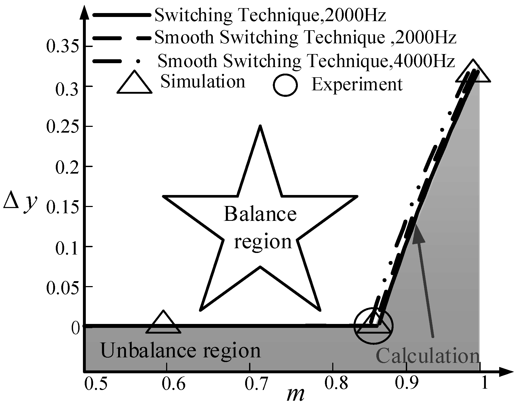
4. Voltage Balance Ability Calculation

The proposed strategy could balance the voltage; however, the ability is not limitless. Thus, the operating region is calculated in this section. Based on the power conservation in Equation (2), the input energy and output energy could be expressed as:
0.5 0 t P W M x V d c i s   d t = C 1 x V c 1 x 2 / 2 | 0 t + C 1 x V c 1 x 2 / 2 | 0 t + ( V c 1 x + V c 2 x ) 2 R x t
Assuming the DC-link voltage keeps constant and is is of unity, the expression of Equation (3) could be simplified as:
0.5 0 t 2 P W M x V d c I sin ω t d t = V d c 2 Y x t
where I is the effective value of is. As Figure 5 shows, the switching technique is easy to be integrated as the PWM of module is symmetric theoretically. Thus, the limitation could be calculated. I is replaced by:
I = j = n j = 1 V d c j 2 Y x / U s
Assuming is is of unity, the active power the grid generates would be consumed on the load completely as:
U N i s = j = n j = 1 V d c x 2 Y x
Define the unbalance degree as:
Δ y = n Y m i n j = 1 n Y j
where the Δy is the unbalance degree, Ymin is the minimum admittance among the modules, from 0 to 1. Δy is 0 when one of the module is no-load. As Un is determined by the switch state of each module, Δy is also determined by the switch state of the module, which owns Ymin. The equation matches only when the switching technique could offer less energy than required by the module of Ymin. That is, in one period of the grid voltage, the DC-link voltage will be balanced if the power which the grid gives to the Ymin could match the power of the Ymin. Otherwise, the DC-link voltage will rise to absorb the power. Thus, the Δy becomes the variable that is used to measure the ability of the voltage balance in the single phase 3LNPC-CR. The less the Δy is, the stronger the voltage balance ability will be. In the instance of module 3, the Δy is described as:
Δ y 2 n V d c 2 U s 1 t 0 t P W M x sin ω t d t 2 n V d c U s 1 π ( 0 1 ω sin 1 1 3 m s 1 sin ω t d t + 1 ω sin 1 1 3 m 1 ω sin 1 1 2 m s 2 sin ω t d t + 1 ω sin 1 2 3 m 1 ω sin 1 1 m s 3 sin ω t d t )
where the S1, S2 and S3 are the integrating region of the PWM, and m is the peak of the modulation waves, which demonstrates the relationship between the Un and Vdc as:
U n = m n V d c
The region from S1 to S4 are illustrated in Figure 7a. The switching technique is based on the modulation of the single phase 3LNPC-CR, which is based on the sin wave. Thus the integrating region could be calculated. Particularly, S1 is −2 and S4 is 0 in Figure 7a. Based on it, the voltage balance ability of the proposed smooth switching technique could be calculated as shown in Figure 7b, where the ORIGINAL part is generated without smooth switching technique, the OPTIMISM part is generated by the smooth switching technique, the ORIGINAL part which is replaced by the OPTIMISM part is shown as ORIGINAL’. By subtracting the ORIGINAL part of Figure 7a and adding the part of the proposed smooth switching technique (ORIGINAL’), the expression of the proposed smooth switching technique could be described as:
Δ y 2 n V d c 2 U s 1 t 0 t P W M x sin ω t d t 2 n V d c U s 1 t ( 0 4 / f P W M x sin ω t d t + 0 1 / f 2 sin ω t d t + 1 / f 2 / f 1 sin ω t d t + 0 + 3 / f 4 / f 1 sin ω t d t )
where f is the switch frequency of the single phase 3LNPC-CR, and Δy’ is the unbalance degree of proposed smooth switching technique. Obviously, the higher frequency the converter owns, the less loss of voltage balance ability it will have, and vice versa. Figure 7c shows the smooth switching technique when the f is 2000 Hz. Then, −2 will not appear in the first quarter of the grid period. However, the higher switch frequency the converter owns, the more switch loss it will suffer.
The results of Δy are shown in Figure 8. As the is is close to 0 at the beginning of the grid period, the price for the optimism is acceptable. The smooth switching technique could keep the DC-link voltage balanced in a three-module 3LNPC-CR at m = 0.82 when the load of one module is removed, which is the same as m = 0.84 with switching technique when the load of one module is removed. Moreover, when m > 0.83, the Δy drops if m rises, which means the ability of voltage balance decrease.

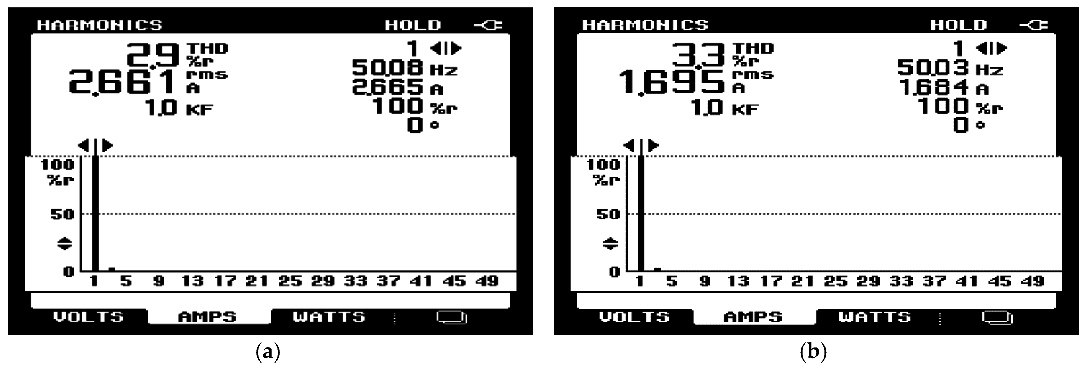
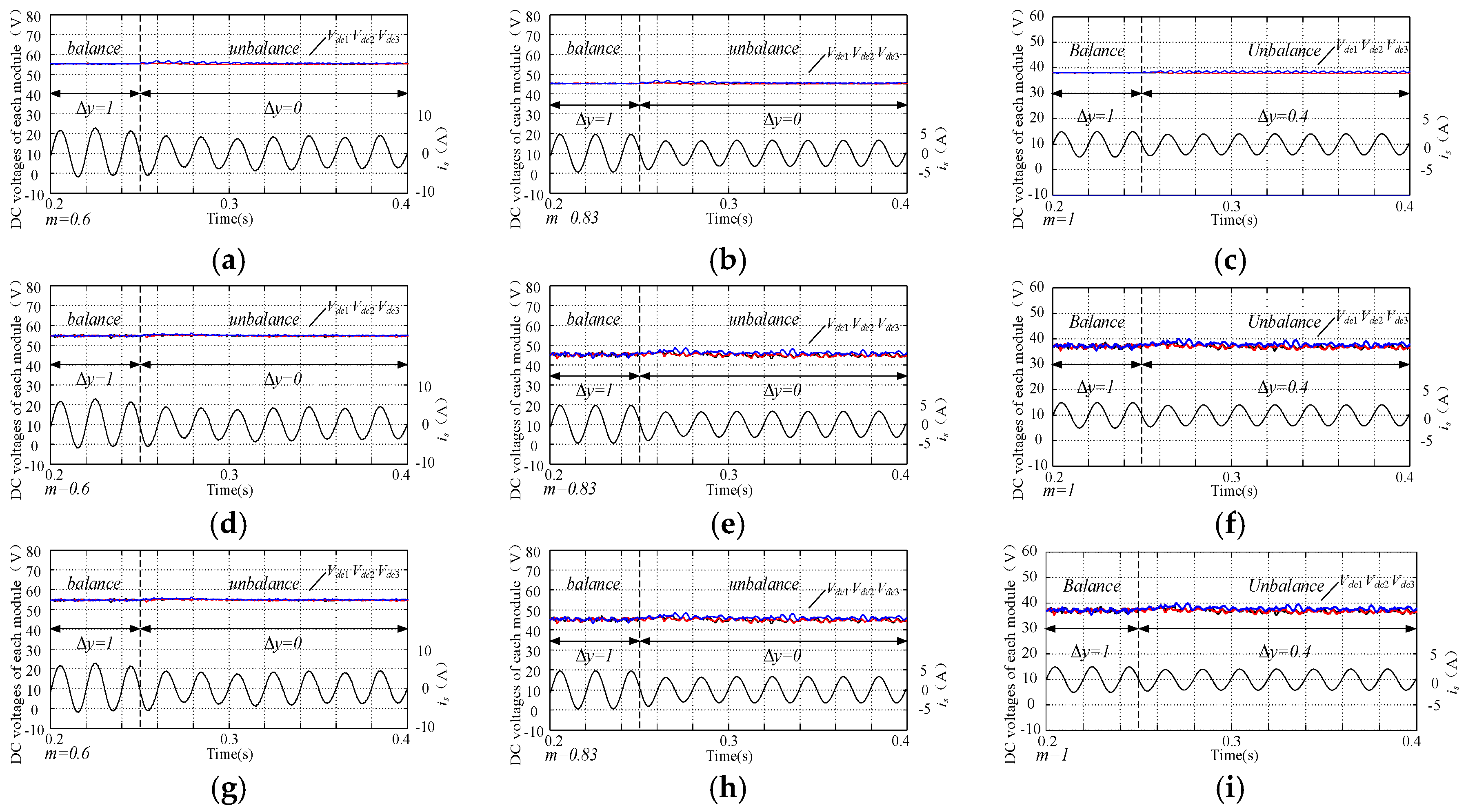
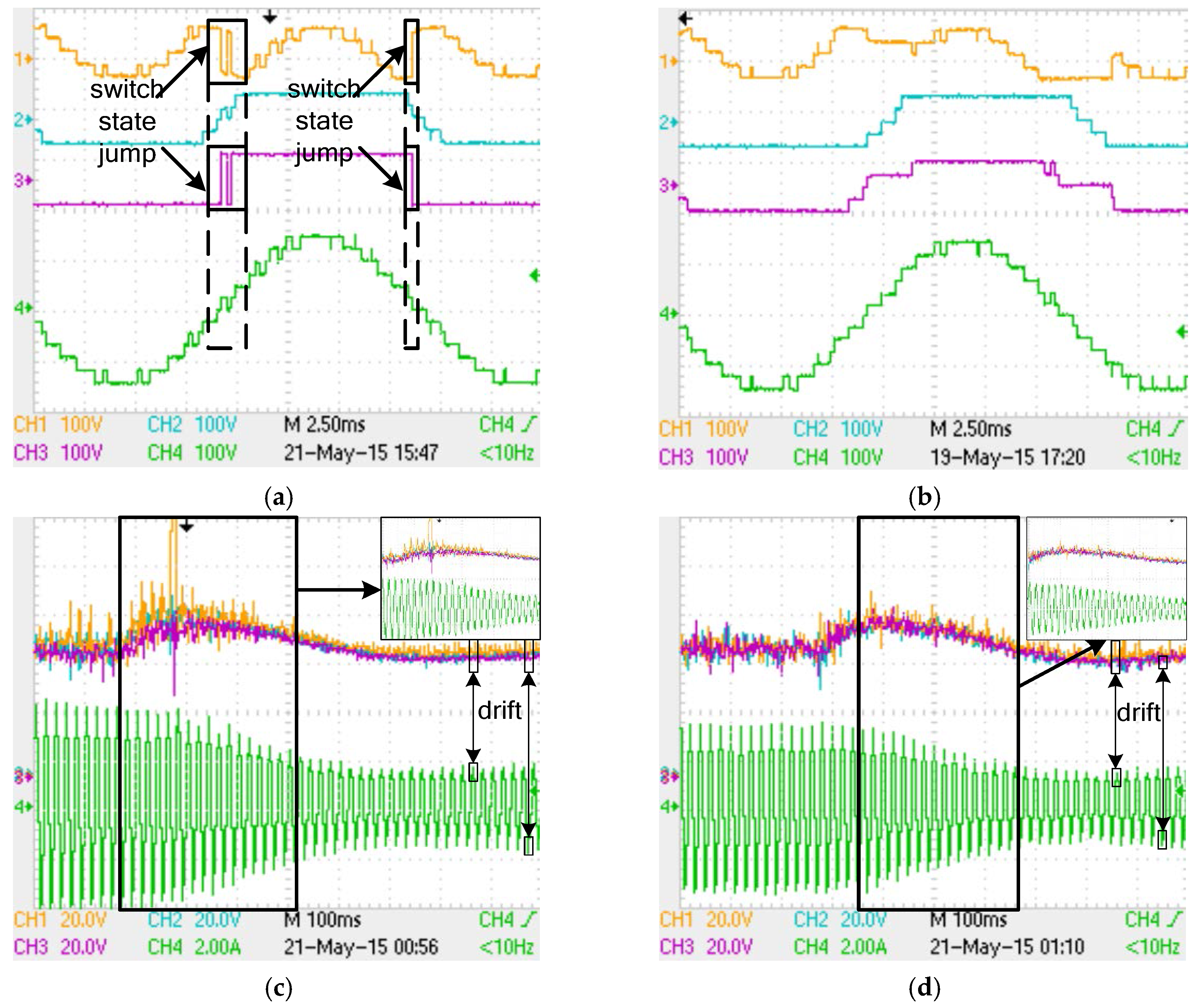
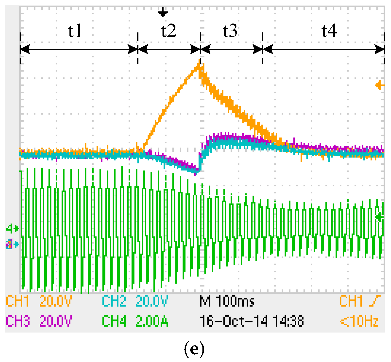
5. Experimental Section

The simulation of 3LNPC-CR based on Matlab/Simulink has been done, which is mainly to verify the voltage balance ability calculation. The simulation parameters are listed in Table 4. The voltage balance ability of switching technique and smooth switching technique are verified, respectively, as seen in Figure 9. Figure 9a–c shows how the switching technique works when m = 0.6, 0.83, and 1, respectively. Based on the calculation result, Δy changes from 1 to 0.4, 1 to 0, as shown in Figure 9a–c, respectively. The DC-link voltage suffers from a slight draft when the 3LNPC-CR works with the unbalance loads. However, it proves that the voltage balance switching technique has been working. The result of smooth switching technique is illustrated in Figure 9d–f, which is generated in the same conditions of Figure 9a–c. The result obeys the curves of the calculations well, but the draft of the DC-link voltage comes to approximately 2%, which is larger than that in Figure 9a–c. This is because the smooth switching technique sacrifices a part of voltage balance ability for smoothing the switch state of 3LNPC module. Figure 9g–i demonstrates the smooth switching technique with the switch frequency of 4000 Hz, which is similar to Figure 9d–f.
The smooth technique has been verified with a three-module 3LNPC-CR. Table 3 shows the experimental circuit parameters. Figure 10a illustrates the output voltage of 3LNPC-CR when the loads of all modules are unbalanced while switching technique is used (Vdc1 > Vdc2 > Vdc3). The switch state will jump between 2 and −2 repeatedly if is changes from positive (negative) to negative (positive). Figure 10b shows the output voltage of 3LNPC-CR when the loads of all modules are unbalanced while smooth switching technique is used (Vdc1 > Vdc2 > Vdc3). Module 1 acquires lower output voltage when is is positive. On the contrary, module 1 acquires higher output voltage when is is negative. Moreover, the output voltage of each module will change smoothly. Figure 10c is the voltage balance limitation of the switching technique, that is, the load of module 1 is removed. Vdc will drift when the switch state jumps. The drift exists because 3LNPC-CR could not afford switch state to release power at the peak and trough of the wave. Progressively, the drift will be enlarged by the instantaneous current at that time. Figure 10d shows the voltage balance limitation of the smooth switching technique, which is same as Figure 10c. As the switch state changes smoothly, the Vdc of smooth switching technique remain steady when the load of module 1 is removed, which is shown in Figure 10d. However, the ability of voltage balance is partially crippled by the rules of smooth switching technique. The drift is more apparent than in the Figure 10c. To verify the dynamic character of the smooth switching technique, the experiment of Figure 10e is designed as follows: in the period of t1, the load of each module is balanced and no voltage balance strategy is used, the voltage keeps balancing as the modulation of 3LNPC-CR is PSC. The load of module 1 is removed in period t2 while no voltage balance strategy is used, the DC-link voltage of module 1 rise dramatically as the analysis of Section 3.1. When the DC-link voltage is higher than 100 V, the smooth switching technique starts to work automatically in the period t3. After 0.2 s, the voltage becomes balanced again in the period t4, as Figure 10 illustrates.
The Total Harmonic Distortion (THD) of Figure 10, with balanced and unbalanced loads, is measured in Figure 11. As the 3LNPC-CR does decrease the THD, the is keeps sinusoidal when the module is balanced (Figure 10a). Although the smooth switching technique rearranges the switch state of each module, the Un of the 3LNPC-CR remain unchanged due to the principle of the smooth switching technique.

6. Conclusions

A smooth switching technique is proposed for balancing the Vdc of 3LNPC-CR in this paper. Based on the simulation and experiment results, the conclusions are made as follows.
First, the voltage balance ability is calculated, and the results are verified by the simulations. Moreover, the experiment result shows that the smooth technique could balance the voltage when the load of one module is removed (modulation depth, m = 0.83). It can be inferred that the smooth switching technique has apparent voltage balance ability when the loads are extremely unequal.
Second, neither switching frequency increases nor switch states jump when the smooth technique is working. The THD (around 3%) of the experiment can verify that the smooth technique is able to control the 3LNPC-CR.
Last, although the unbalance makes the Vdc increase dramatically, the voltage could draw back within 0.2 s once the smooth switching technique is operated. The dynamic character of smooth switching technique is demonstrated, as the Vdc recovers quickly in some serious situations.

Acknowledgments

This work was supported by the National Natural Science Foundation of China (Grant Nos. 51477144, and 51377004).

Author Contributions

Xu Peng and Xiaoqiong He conceived the strategy and the experiments; Aiping Guo performed the experiments; Zeliang Shu analyzed the data; Shibin Gao contributed experiment prototype; and Pengcheng Han wrote the paper.

Conflicts of Interest

The authors declare no conflict of interest.

References

  1. Peng, H.; Hagiwara, M.; Akagi, H. Modeling and analysis of switching-ripple voltage on the DC Link between a diode rectifier and a modular multilevel cascade inverter (MMCI). IEEE Trans. Power Electron. 2013, 28, 75–84. [Google Scholar] [CrossRef]
  2. McGrath, B.P.; Holmes, D.G. Multicarrier PWM strategies for multilevel inverters. IEEE Trans. Ind. Electron. 2002, 49, 858–867. [Google Scholar] [CrossRef]
  3. Kouro, S.; Malinowski, M.; Gopakumar, K.; Pou, J.; Franquelo, L.G.; Wu, B.; Rodriguez, J.; Perez, M.A.; Leon, J.I. Recent advances and industrial applications of multilevel converters. IEEE Trans. Ind. Electron. 2010, 57, 2553–2580. [Google Scholar] [CrossRef]
  4. He, X.; Shu, Z.; Peng, X.; Zhou, Q.; Zhou, Y.; Zhou, Q.; Gao, S. Advanced cophase traction power supply system based on three-phase to single-phase converter. IEEE Trans. Power Electron. 2014, 29, 5323–5333. [Google Scholar] [CrossRef]
  5. Zhao, C.; Dujic, D.; Mester, A.; Steinke, J.K.; Weiss, M.; Lewdeni-Schmid, S.; Chaudhuri, T.; Stefanutti, P. Power electronic traction transformer-medium voltage prototype. IEEE Trans. Ind. Electron. 2014, 61, 3257–3268. [Google Scholar] [CrossRef]
  6. She, X.; Huang, A.Q. Current sensorless power balance strategy for DC/DC converters in a cascaded multilevel converter based solid state transformer. IEEE Trans. Ind. Electron. 2014, 29, 17–22. [Google Scholar] [CrossRef]
  7. He, X.Q.; Guo, A.P.; Peng, X.; Zhou, Y.Y.; Shi, Z.H.; Shu, Z.L. A traction three-phase to single-phase cascade converter substation in an advanced traction power supply system. Energies 2015, 8, 9915–9929. [Google Scholar] [CrossRef]
  8. Vahedi, H.; Al-Haddad, K. A novel multilevel multi-output bidirectional active buck PFC rectifier. IEEE Trans. Ind. Electron. 2016, 63, 5442–5450. [Google Scholar] [CrossRef]
  9. Vahedi, H.; Philippe-Alexandre, L.; Al-Haddad, K. Balancing three-level NPC inverter DC bus using closed-loop SVM: Real time implementation and investigation. IET Power Electron. 2016, 9, 2076–2084. [Google Scholar] [CrossRef]
  10. Zou, R. Simulation study on transient current control of four quadrant converter. Electr. Drive Locomot. 2003, 6, 17–20. [Google Scholar]
  11. Shu, Z.; Zhu, H.; He, X.; Ding, N.; Jing, Y. One-inductor-based auxiliary circuit for DC-link capacitor voltage equalisation of diode-clamped multilevel converter. IET Power Electron. 2013, 6, 1339–1349. [Google Scholar] [CrossRef]
  12. Zhu, H.; Shu, Z.; Gao, F.; Qin, B.; Gao, S. Five-level diode-clamped active power filter using voltage space vector-based indirect current and predictive harmonic control. IET Power Electron. 2014, 7, 713–723. [Google Scholar] [CrossRef]
  13. Tallam, R.M.; Rajendra, N.; Nondahl, T.A. A carrier-based PWM scheme for neutral-point voltage balancing in three-level inverters. IEEE Trans. Ind. Appl. 2005, 41, 1734–1743. [Google Scholar] [CrossRef]
  14. Cobreces, S.; Bordonau, J.; Salaet, J.; Bueno, E.J.; Rodriguez, F.J. Exact linearization nonlinear neutral-point voltage control for single-phase three-level NPC converters. IEEE Trans. Power Electron. 2009, 24, 2357–2362. [Google Scholar] [CrossRef] [Green Version]
  15. Shu, Z.; Ding, N.; Chen, J.; Zhu, H.; He, X. Multilevel SVPWM with DC-Link capacitor voltage balancing control for diode-clamped multilevel converter based STATCOM. IEEE Trans. Ind. Electron. 2013, 60, 1884–1896. [Google Scholar] [CrossRef]
  16. Dujic, D.; Zhao, C.; Mester, A.; Steinke, J.K.; Weiss, M.; Lewdeni-Schmid, S.; Chaudhuri, T.; Stefanutti, P. Power electronic traction transformer-low voltage prototype. IEEE Trans. Power Electron. 2013, 28, 5522–5534. [Google Scholar] [CrossRef]
  17. Dell’Aquila, A.; Liserre, M.; Monopoli, V.G.; Rotondo, P. Overview of PI-based solutions for the control of DC buses of a single-phase H-bridge multilevel active rectifier. IEEE Trans. Ind. Appl. 2008, 44, 857–866. [Google Scholar] [CrossRef]
  18. Zhao, T.; Wang, G.; Bhattacharya, S.; Huang, A.Q. Voltage and power balance control for a cascaded H-bridge converter-based solid-state transformer. IEEE Trans. Power Electron. 2013, 28, 1523–1532. [Google Scholar] [CrossRef]
  19. Iman-Eini, H.; Schanen, J.L.; Farhangi, S.; Roudet, J. A modular strategy for control and voltage balancing of cascaded H-bridge rectifiers. IEEE Trans. Power Electron. 2008, 23, 2428–2442. [Google Scholar] [CrossRef]
  20. Moosavi, M.; Farivar, G.; Iman-Eini, H.; Shekarabi, S.M. A voltage balancing strategy with extended operating region for cascaded-bridge converters. IEEE Trans. on Power. Electron. 2014, 29, 5044–5053. [Google Scholar] [CrossRef]
  21. She, X.; Huang, A.Q.; Wang, G. 3-D space modulation with voltage balancing capability for a cascaded seven-level converter in a solid-state transformer. IEEE Trans. Power Electron. 2011, 26, 3778–3789. [Google Scholar] [CrossRef]
  22. Vazquez, S.; Leon, J.I.; Franquelo, L.G.; Padilla, J.J.; Carrasco, J.M. DC-voltage-ratio control strategy for multilevel cascaded converters fed with a single DC source. IEEE Trans. Ind. Electron. 2009, 3, 2513–2521. [Google Scholar] [CrossRef]
Figure 1. Configuration of the three-level neutral point clamped cascaded rectifier (3LNPC-CR): (a) Topology of 3LNPC-CR; and (b) Control system of 3LNPC-CR.
Energies 09 00803 g001
Figure 2. Output voltage of SP and SN: (a) The switch state 00, SP; (b) The switch state 01, SP; (c) The switch state 10, SN; and (d) The switch state 11, SN. SP: small positive switch states; SN: small negative switch states.
Energies 09 00803 g002
Figure 3. Principle of fluctuation balance strategy (after optimism): (a) PWMx = 1; and (b) PWMx = −1. Sp: register of SP; sn: register of SN.
Energies 09 00803 g003
Figure 4. Output Voltage of the three-level neutral point clamped converter (3LNPC). (ai) Switch states I–IX.
Energies 09 00803 g004
Figure 5. Proposed smooth switching technique of module x.
Energies 09 00803 g005
Figure 6. Modulation of switching technique: (a) Switching technique; and (b) Smooth switching technique.
Energies 09 00803 g006aEnergies 09 00803 g006b
Figure 7. Modulation of switching technique: (a) Switching technique; (b) Smooth switching technique (4000 Hz); and (c) Smooth switching technique (2000 Hz).
Energies 09 00803 g007aEnergies 09 00803 g007b
Figure 8. Result of unbalance degree calculation.
Energies 09 00803 g008
Figure 9. Simulation results: (a) m = 0.6, switching technique, Δy from 1 to 0, f = 2000 Hz; (b) m = 0.83, switching technique, Δy from 1 to 0, f = 2000 Hz; (c) m = 1, switching technique, Δy from 1 to 0.4, f = 2000 Hz; (d) m = 0.6, smooth switching technique, Δy from 1 to 0, f = 2000 Hz; (e) m = 0.83, smooth switching technique, Δy from 1 to 0, f = 2000 Hz; (f) m = 1, smooth switching technique, Δy from 1 to 0.4, f = 2000 Hz; (g) m = 0.6, smooth switching technique, Δy from 1 to 0, f = 4000 Hz; (h) m = 0.83, smooth switching technique, Δy from 1 to 0, f = 4000 Hz; and (i) m = 1, smooth switching technique, Δy from 1 to 0.4, f = 4000 Hz.
Energies 09 00803 g009
Figure 10. Experimental results: (a) Output voltage when the loads of module are unbalanced using switching technique (CH1: Un1, CH2: Un2, CH3: Un3, CH4: UN); (b) Output voltage when the loads are unbalanced using smooth switching technique (CH1: Un1, CH2: Un2, CH3: Un3, CH4: UN); (c) Dynamic waveform using switching technique when the load of module 1 is removed (CH1: Vdc1, CH2: Vdc2, CH3: Vdc3, CH4: is); (d) Dynamic waveform using smooth switching technique when the load of module 1 is removed (CH1: Vdc1, CH2: Vdc2, CH3: Vdc3, CH4: is); and (e) Dynamic waveform of step changes experiment using smooth switching technique (CH1: Vdc1, CH2: Vdc2, CH3: Vdc3, CH4: is). CH: Channel of Oscilloscope.
Energies 09 00803 g010aEnergies 09 00803 g010b
Figure 11. Total Harmonic Distortion (THD) results: (a) All modules are balanced; and (b) The load of module 3 is removed.
Energies 09 00803 g011
Table 1. Switch states of Figure 2. SP: small positive switch states; SN: small negative switch states.
MODEisunVc1Vc2Register
00>0Vc1, 0.5Vdcchargeno effectSP
<0Vc1, 0.5Vdcdischargeno effect
01>0Vc2, 0.5Vdcno effectchargeSP
<0Vc2, 0.5Vdcno effectdischarge
10>0Vc2, −0.5Vdcno effectdischargeSN
<0Vc2, −0.5Vdcno effectcharge
11>0Vc1, −0.5Vdcdischargeno effectSN
<0Vc1, −0.5Vdcchargeno effect
Table 2. Basic principle of fluctuation balance strategy. Sp: register of SP sn: register of SN.
Case V c 1 > V c 2 , i s > 0 V c 1 > V c 2 , i s < 0 V c 1 < V c 2 , i s > 0 V c 1 < V c 2 , i s > 0
Register spsp = 01sp = 00sp = 00sp = 01
Register snsn = 11sn = 10sn = 10sn = 11
Table 3. Switching Technique Generator.
CaseV1VbVsVs+1Vn
is > 0−2−2PWMs22
is < 022PWMs−2−2
Table 4. Sequence pulse generator.
Parameter NameParameter ValueNumbers
Voltage source75 V/50 Hz1
Filter inductance1 mL1
DC-link voltage (Vdc)38–55 V3
DC-link capacitor1880 μF6
Output power114–360 W1
Carrier wave frequency750 Hz-
Carrier wave frequency1500 Hz
Inductance of filter1 mL
Capacitance of filter2200 μF
Number of modules3

