
Integrated Three-Voltage-Booster DC-DC Converter to Achieve High Voltage Gain with Leakage-Energy Recycling for PV or Fuel-Cell Power Systems

Abstract
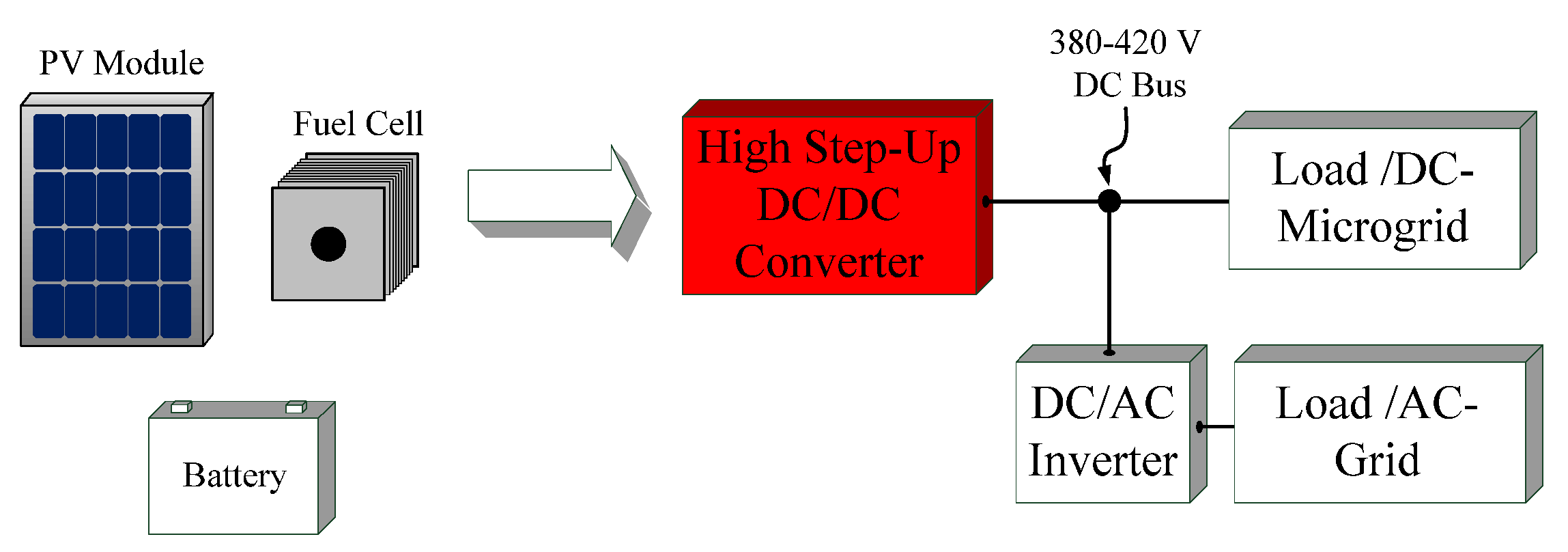
:1. Introduction


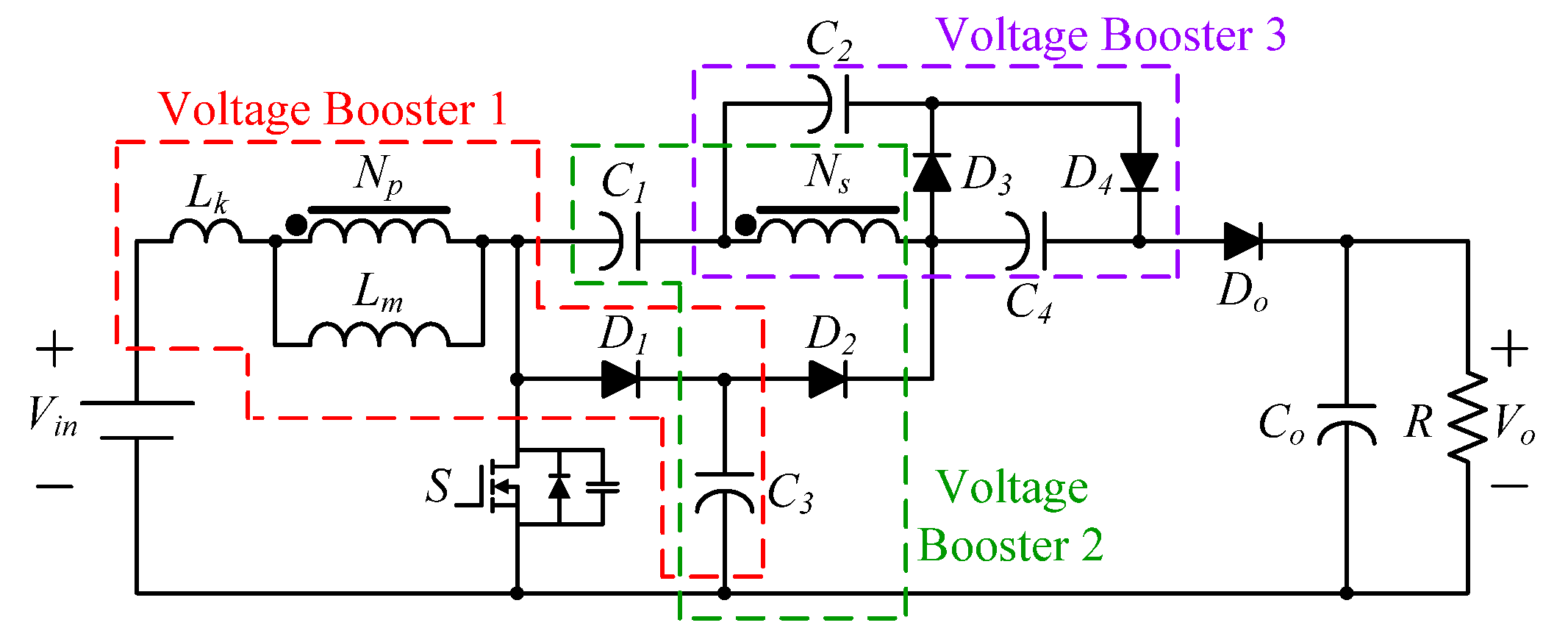
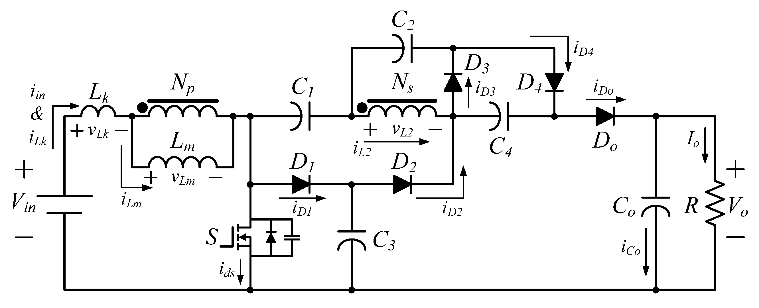
2. Operation Principle of the Proposed Converter

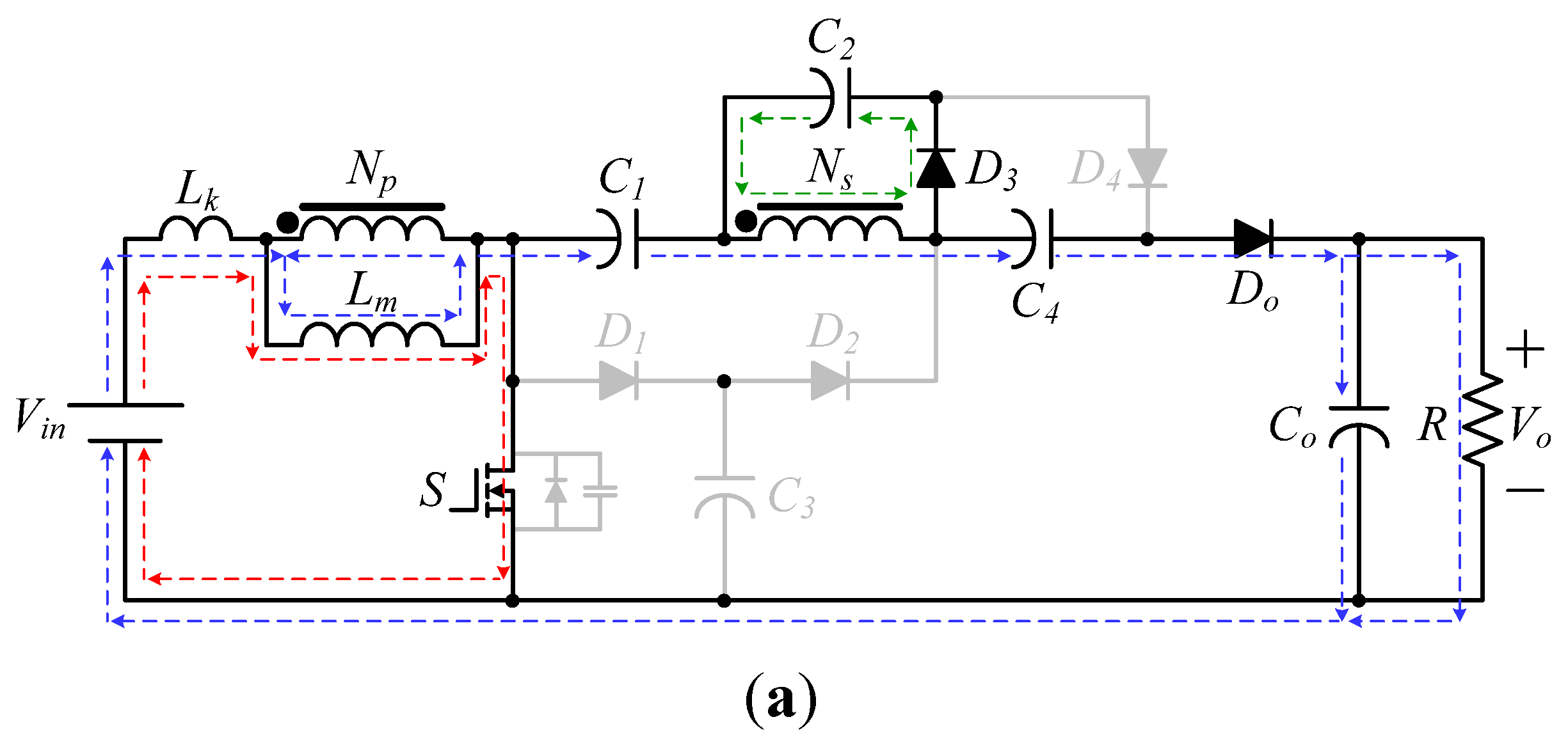
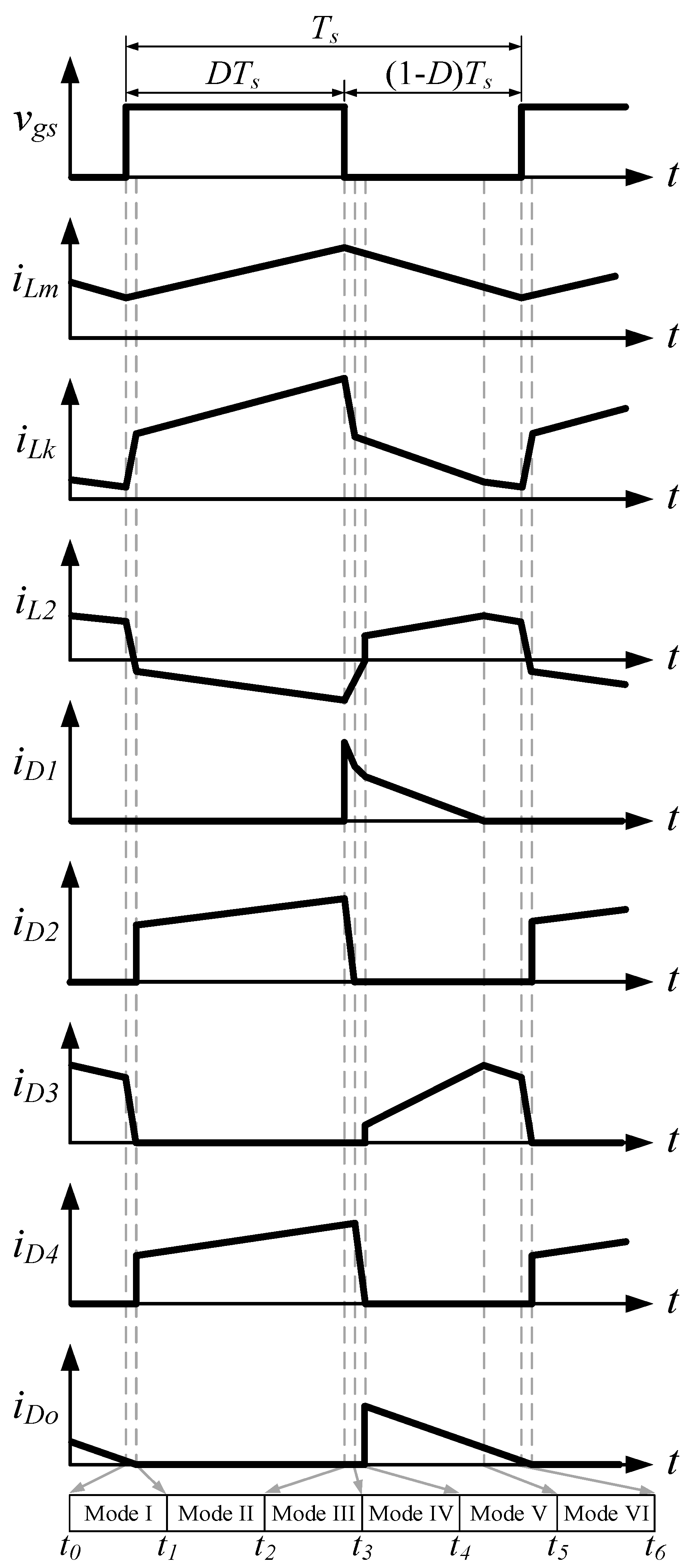
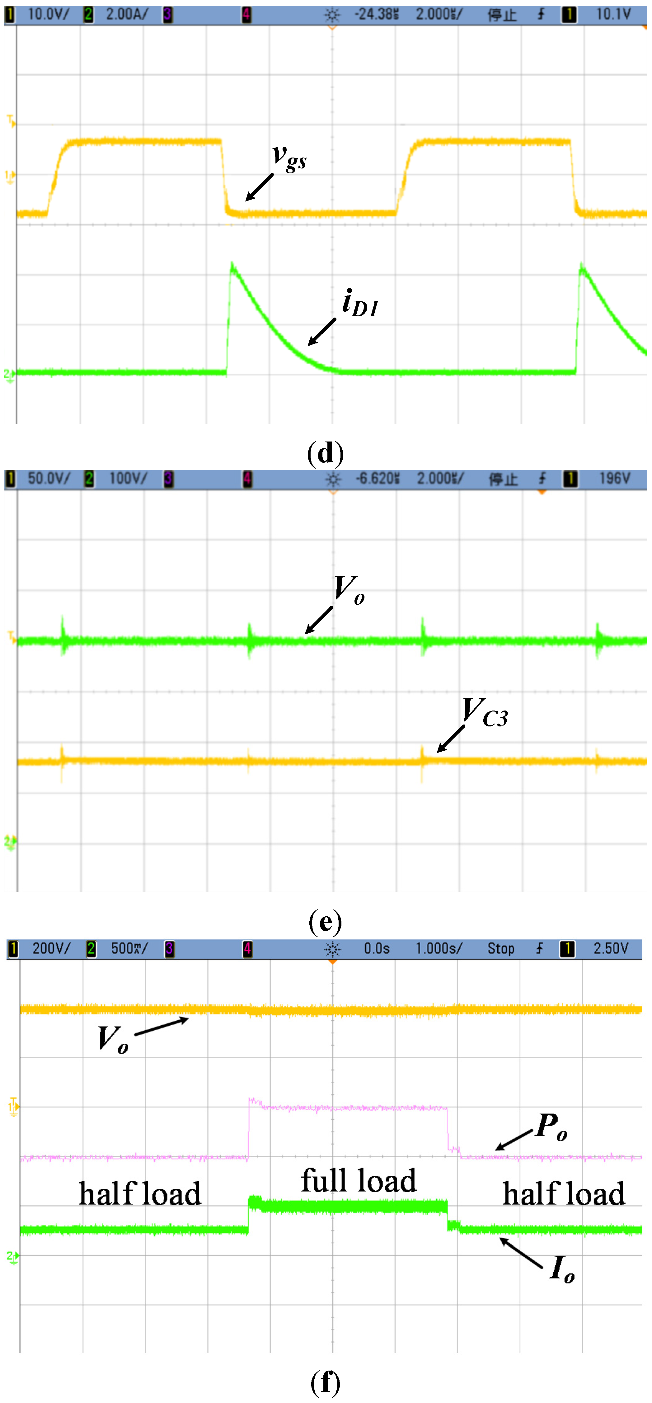
- Stage 1 [t0~t1]: At time t = t0, switch S is turned on. Diodes D1, D2 and D4 are reversely biased, but D3 and Do are forward biased. In this time interval, the current of leakage-inductor iLk increases linearly and steeply. The energy stored in magnetizing-inductor Lm is released to the output via Do and boosts capacitor C2 via D3. Meanwhile, the current following through Do, iDo, is decreasing. Until the current iDo drops to zero, this operation stage ends. There is no reverse-recovery loss on diode Do. Figure 4a shows the equivalent circuit of this stage.
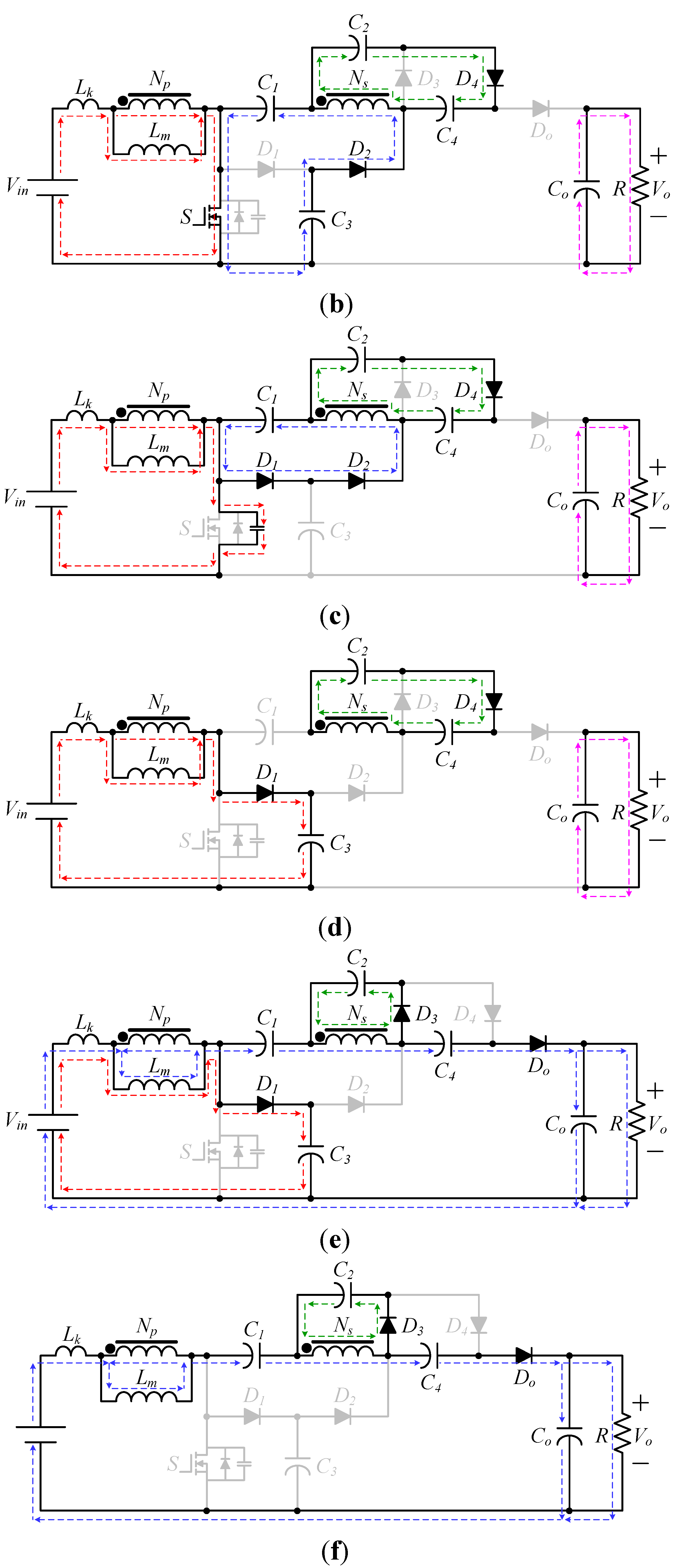
- Stage 2 [t1~t2]: This stage begins at time t = t1, of which equivalent circuit is shown in Figure 4b. Switch S remains closed. Diodes D1, D3 and Do are reversely biased, but D2 and D4 are forward biased. In this time interval, the magnetizing-inductor Lm and leakage-inductor Lk absorb energy from the DC source Vin. The switched capacitor C1 is charged by the secondary of the coupled inductor and capacitor C3, while the other switched capacitor C4 is by the secondary of the coupled inductor and capacitor C2. During this stage, only the output capacitor Co provides energy to the load R. When switch S is turned off, operation of this converter enters into the next stage.
- Stage 3 [t2~t3]: Switch S is turned off at t = t2. During this stage, diodes D1, D2 and D4 are in on-state, but diodes D3 and Do are reversely biased. In this time interval, the energy of leakage-inductor Lk releases to the parasitic capacitor of switch S and thus, switch voltage increases. When the voltage across the parasitic capacitor is higher than that of boosting capacitor C3, diode D1 becomes forward and this operation stage is completed. Figure 4c illustrates the corresponding equivalent of Stage 3.
- Stage 4 [t3~t4]: Switch S is still kept in off-state over the period of Stage 4. Diodes D2, D3 and Do are reversely biased, but diodes D1, and D4 are in forward bias, as shown in Figure 4d. The boosting capacitor C3 is charged by magnetizing-inductor Lm and leakage-inductor Lk. That is, leakage energy of Lk is recycled to C3 and the voltage across active switch is clamped by C3, which suppresses voltage spike effectively. At the moment the voltage polarity of magnetizing-inductor Lm changes, this stage is finished.
- Stage 5 [t4~t5]: The equivalent circuit is illustrated in Figure 4e. Switch S remains off. The status of diodes D1, D3 and Do are on but D2 and D4 off. In this time interval, the energy of magnetizing-inductor Lm is dumped to ideal transformer, output terminal, and capacitor C3 simultaneously. The secondary side of coupled inductor charges the boosting capacitor C2 via diode D3. At the same time, the output voltage is stacked by input voltage Vin, coupled inductor, and capacitors C1 and C4.
- Stage 6 [t5~t6]: This stage begins as C3 stops charging. The diode D1 becomes reversely biased. The corresponding equivalent circuit is shown in Figure 4f. The energy stored in Lm keeps dumping energy to C2 via ideal transformer. When power switch is turned on again, this stage ends and converter operation over one switching cycle is completed.


3. Steady-State Analysis of the Proposed Converter
- (1)
- The values of all capacitors are large enough so that voltages across all capacitors are considered as constant;
- (2)
- All semiconductor components in the power circuit are ideal;
- (3)
- The magnetizing inductance is much greater than leakage inductance. The influence of the leakage inductance can be neglected. That is, the coupling coefficient of coupled inductor k is equal to unity;
- (4)
- Equivalent series resistance of coupled inductor is ignored;
- (5)
- The active switch is closed for DTs and open for (1-D)Ts;
- (6)
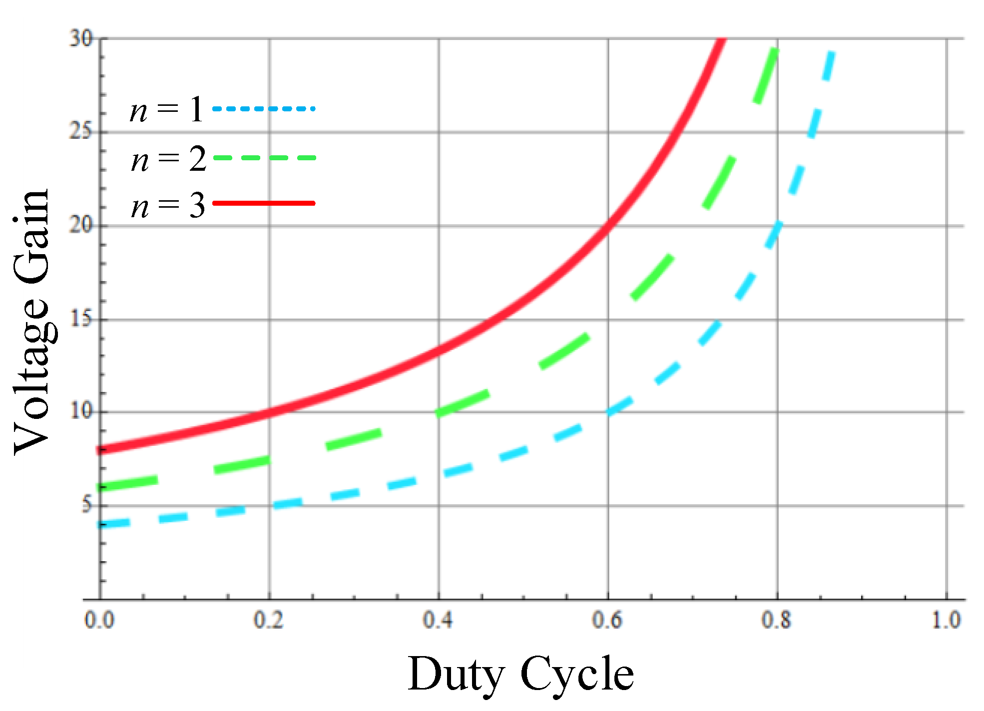
3.1. Derivation of Voltage Gain


3.2. Voltage Stress of Power Device
3.3. Current on Power Devices
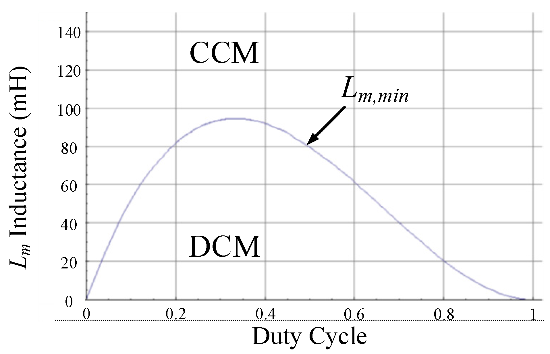
3.4. Design of Energy Storage Component
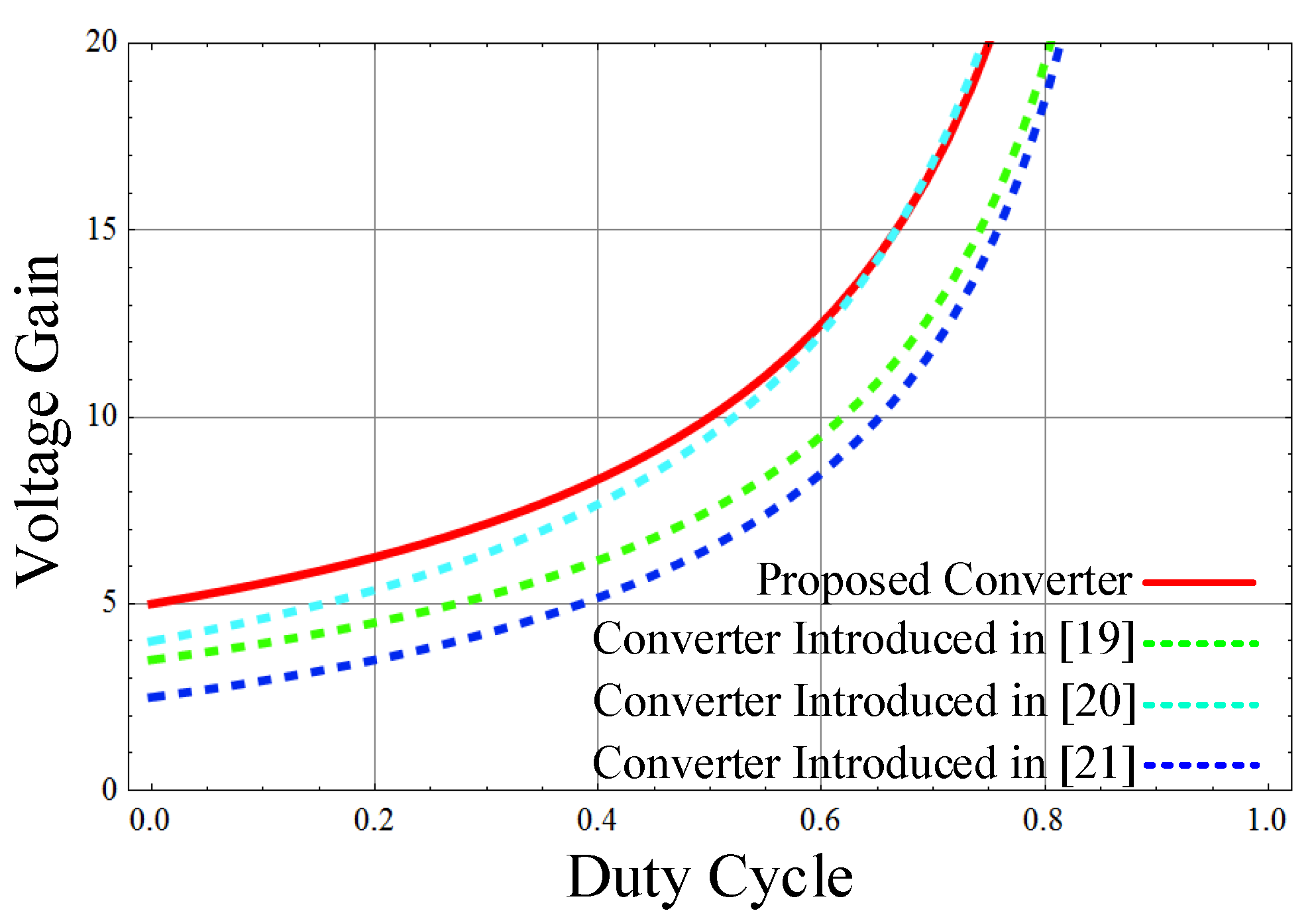
3.5. Performance Comparison

| High step-up converters | Converter introduced in [19] | Converter introduced in [20] | Converter introduced in [21] | Proposed converter |
|---|---|---|---|---|
| Voltage gain | ||||
| Diodes | 3 | 6 | 5 | 5 |
| Capacitors | 3 | 6 | 5 | 5 |
| windings | 2 | 2 | 3 | 2 |
| Voltage stress on switch | ||||
| Conduction loss | small | middle | small | small |
| Switching loss | small | middle | middle | small |
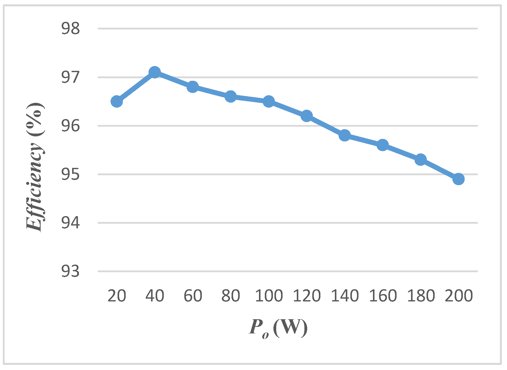
4. Experimental Results

| Symbols | Values & Types |
|---|---|
| Vin (Input voltage) | 36 V |
| Vo (Output voltage) | 400 V |
| Po (Rated power) | 200 W |
| fs (Switching frequency) | 100 kHz |
| Lm (Magnetizing inductance) | 55 μH |
| Lk (Leakage inductance) | 1.03 μH |
| n (Transformer turns ratio) | 1:1.6 |
| C1 and C4 (Capacitance) | 33 μF |
| C2 and C3 (Capacitance) | 22 μF |
| Co (Capacitance) | 82 μF |
| S (Active switch) | IRFSL4615PbF (150 V/33 A) |
| D1 (Diode) | BYW29E-200 (200 V/8 A) |
| D2, D3, D4, and Do (Diodes) | 8ETH03PBF (300 V/8 A) |
5. Conclusions
Acknowledgments
Author Contributions
Conflicts of Interest
References
- Wang, Z.; Li, H. Integrated MPPT and bidirectional battery charge for PV application using one multiphase interleaved three-port DC-DC converter. In Proceedings of the Applied Power Electronics Conference and Exposition, Fort Worth, TX, USA, 6–11 March 2011; pp. 295–300.
- Eid, A. Utility integration of PV-wind-fuel cell hybrid distributed generation systems under variable load demands. Int. J. Electr. Power Energy Syst. 2014, 62, 689–699. [Google Scholar] [CrossRef]
- Lu, D.C.; Cheng, K.W.; Lee, Y.S. A single-switch continuous-conduction-mode boost converter with reduced reverse-recovery and switch losses. IEEE Trans. Ind. Electron. 2003, 50, 767–776. [Google Scholar] [CrossRef]
- Bryant, B.; Kazimiercuuk, M.K. Voltage-loop power stage transfer functions with MOSFET delay for boost PWM converter operating in CCM. IEEE Trans. Ind. Electron. 2007, 54, 347–353. [Google Scholar] [CrossRef]
- Da Silva, E.S.; Barbosa, L.D.R.; Vieira, J.B.; de Freitas, L.C.; Farias, V.J. An improved boost PWM soft-single-switched converter with low voltage and current stresses. IEEE Trans. Ind. Electron. 2001, 48, 1174–1179. [Google Scholar] [CrossRef]
- Jovanovic, M.M.; Jang, Y. A new soft-switched boost converter with isolated active snubber. IEEE Trans. Ind. Appl. 1999, 35, 496–502. [Google Scholar] [CrossRef]
- Roh, C.W.; Han, S.H.; Youn, M.J. Dual coupled inductor fed isolated boost converter for low input voltage applications. Electron. Lett. 1999, 35, 1791–1792. [Google Scholar] [CrossRef]
- Papanikolaou, N.P.; Tatakis, E.C. Active voltage clamp in flyback converters operating in CCM mode under wide load variation. IEEE Trans. Ind. Electron. 2004, 51, 632–640. [Google Scholar] [CrossRef]
- Wang, C.M. A novel ZCS-PWM flyback converter with a simple ZCS-PWM commutation cell. IEEE Trans. Ind. Electron. 2008, 55, 749–757. [Google Scholar] [CrossRef]
- Lin, B.R.; Hsieh, F.Y. Soft-switching zeta-flyback converter with a buck-boost type of active clamp. IEEE Trans. Ind. Electron. 2007, 54, 2813–2822. [Google Scholar]
- Yang, L.S.; Liang, T.J.; Chen, J.F. Transformerless DC-DC converter with high step-up voltage gain. IEEE Trans. Ind. Electron. 2009, 56, 3144–3152. [Google Scholar] [CrossRef]
- Axelorod, B.; Berkovic, Y.; Ioinovici, A. Transformerless DC-DC converters with a very high DC line-to-load voltage ratio. In Proceeding of the 2003 International Symposium on Circuits and Systems, Bangkok, Thailand, 25–28 May 2003; Volume 3, pp. III-435–III-438.
- Shu, L.J.; Liang, T.J.; Yang, L.S.; Lin, R.L. Transformerless high step-up DC-DC converter using cascode technique. In Proceedings of the 2010 International Power Electronics Conference, Sapporo, Japan, 21–24 June 2010; pp. 63–67.
- Young, C.M.; Chen, M.H.; Chang, T.A.; Ko, C.C. Transformerless high step-up DC-DC converter with cockcroft-walton voltage multiplier. In Proceedings of the 2011 6th IEEE Conference on Industrial Electronics and Applications, Beijing, China, 21–23 June 2011; pp. 1599–1604.
- Sabzali, A.J.; Ismail, E.H.; Behbehani, H.M. High voltage step-up integrated double Boost-Sepic DC-DC converter for fuel-cell and photovoltaic applications. Renew. Energy 2015, 82, 44–53. [Google Scholar] [CrossRef]
- Al-Saffar, M.A.; Ismail, E.H. A high voltage ratio and low stress DC-DC converter with reduced input current ripple for fuel cell source. Renew. Energy 2015, 82, 35–43. [Google Scholar] [CrossRef]
- Nouri, T.; Babaei, E.; Hosseini, S.H. A generalized ultra step-up DC-DC converter for high voltage application with design considerations. Electr. Power Syst. Res. 2013, 105, 71–84. [Google Scholar] [CrossRef]
- Patidar, K.; Umarikar, A.C. High step-up converters based on quadratic boost converter for micro-inverter. Electr. Power Syst. Res. 2015, 119, 168–177. [Google Scholar] [CrossRef]
- Laird, I.; Lu, D.D. High Step-up DC/DC topology and MPPT algorithm for use with a thermoelectric generator. IEEE Trans. Power Electron. 2013, 28, 3147–3157. [Google Scholar] [CrossRef]
- Hsieh, Y.; Chen, J.; Liang, T.; Yang, L. Novel high step-up DC-DC converter with coupled-inductor and switched capacitor technique for a sustainable energy system. IEEE Trans. Power Electron. 2011, 26, 3481–3490. [Google Scholar] [CrossRef]
- Changchien, S.; Liang, T.; Chen, J.; Yang, L. Novel high step-up DC-DC converter for fuel cell energy conversion system. IEEE Trans. Ind. Electron. 2010, 57, 2007–2017. [Google Scholar] [CrossRef]
© 2015 by the authors; licensee MDPI, Basel, Switzerland. This article is an open access article distributed under the terms and conditions of the Creative Commons Attribution license (http://creativecommons.org/licenses/by/4.0/).
Share and Cite
Shen, C.-L.; Chen, H.-Y.; Chiu, P.-C. Integrated Three-Voltage-Booster DC-DC Converter to Achieve High Voltage Gain with Leakage-Energy Recycling for PV or Fuel-Cell Power Systems. Energies 2015, 8, 9843-9859. https://doi.org/10.3390/en8099843
Shen C-L, Chen H-Y, Chiu P-C. Integrated Three-Voltage-Booster DC-DC Converter to Achieve High Voltage Gain with Leakage-Energy Recycling for PV or Fuel-Cell Power Systems. Energies. 2015; 8(9):9843-9859. https://doi.org/10.3390/en8099843
Chicago/Turabian StyleShen, Chih-Lung, Hong-Yu Chen, and Po-Chieh Chiu. 2015. "Integrated Three-Voltage-Booster DC-DC Converter to Achieve High Voltage Gain with Leakage-Energy Recycling for PV or Fuel-Cell Power Systems" Energies 8, no. 9: 9843-9859. https://doi.org/10.3390/en8099843