Article

Novel Step-Down DC–DC Converters Based on the Inductor–Diode and Inductor–Capacitor–Diode Structures in a Two-Stage Buck Converter

by
Mauricio Dalla Vecchia
1,2,*,
Giel Van den Broeck
1,2,
Simon Ravyts
1,2 and
Johan Driesen
1,2
1
Departement Elektrotechniek, KU Leuven, Kasteelpark Arenberg 10, 3001 Leuven, Belgium
2
EnergyVille, Thor Park 8310, 3600 Genk, Belgium
*
Author to whom correspondence should be addressed.
Energies 2019, 12(6), 1131; https://doi.org/10.3390/en12061131
Submission received: 14 January 2019 / Revised: 5 March 2019 / Accepted: 19 March 2019 / Published: 22 March 2019
(This article belongs to the Special Issue Design and Control of Power Converters 2019)

Abstract

:
This paper explores and presents the application of the Inductor–Diode and Inductor-Capacitor-Diode structures in a DC–DC step-down configuration for systems that require voltage adjustments. DC micro/picogrids are becoming more popular nowadays and the study of power electronics converters to supply the load demand in different voltage levels is required. Multiple strategies to step-down voltages are proposed based on different approaches, e.g., high-frequency transformer and voltage multiplier/divider cells. The key question that motivates the research is the investigation of the aforementioned Inductor–Diode and Inductor–Capacitor–Diode, current multiplier/divider cells, in a step-down application. The two-stage buck converter is used as a study case to achieve the output voltage required. To extend the intermediate voltage level flexibility in the two-stage buck converter, a second switch was implemented replacing a diode, which gives an extra degree-of-freedom for the topology. Based on this modification, three regions of operation are theoretically defined, depending on the operational duty cycles δ2 and δ1 of switches S2 and S1. The intermediate and output voltage levels are defined based on the choice of the region of operation and are mapped herein, summarizing the possible voltage levels achieved by each configuration. The paper presents the theoretical analysis, simulation, implementation and experimental validation of a converter with the following specifications; 48 V/12 V input-to-output voltage, different intermediate voltage levels, 100 W power rating, and switching frequency of 300 kHz. Comparisons between mathematical, simulation, and experimental results are made with the objective of validating the statements herein introduced.

1. Introduction

In the last century, AC systems predominated as the most widespread method for energy generation, transmission, and distribution. For regular AC generation, large power plants, e.g., coal, hydro, and nuclear, have been used to centrally generate energy. Alternatives, such as wind and solar generation, are more frequently being installed to decentralize the energy production and lower the CO2 emitted by the energy production [1,2].
Wind farms (AC generation) are more common in remote regions (on and off-shore) where the wind is conducive for generation. Solar (DC generation), on the other hand, started to become viable for application in high populated areas where the sun irradiation is high enough to achieve maximum power generation. DC systems started to be developed and implemented in pilot projects and real applications because they have proved to be more efficient than AC systems in terms of transformation steps [3], costs [4], and power transfer capability [5]. Applications of DC system such as in micro- and nanogrids [6,7], datacenters [8,9], and aircrafts, where redundancy and backup is mandatory, are currently on the rise. DC system technology can also be implemented in isolated/remote/emerging regions [10]. In these systems, redundancy normally is indispensable in order to keep the system operational even if a component and/or a converter fails. Furthermore, DC loads are common especially in low voltage/low power applications, for instance, in computer and battery chargers, USB and USB-C ports, and LED lights. These type of loads are commonly found in offices and residences.
Discussions among the voltage levels that are implemented in these systems are extensively presented in the literature [11], for instance, with a voltage between 350 and 400 V for distribution in unipolar or bipolar [6,12,13] DC configurations to supply high power equipments. The 48 V level is [14,15] normally adopted as an intermediate bus stage to supply the low voltage/low power loads aforementioned. The 48 V level is also getting more common in battery systems for Electric Vehicles (EV), and it is considered for residential applications due to its user safety approach.
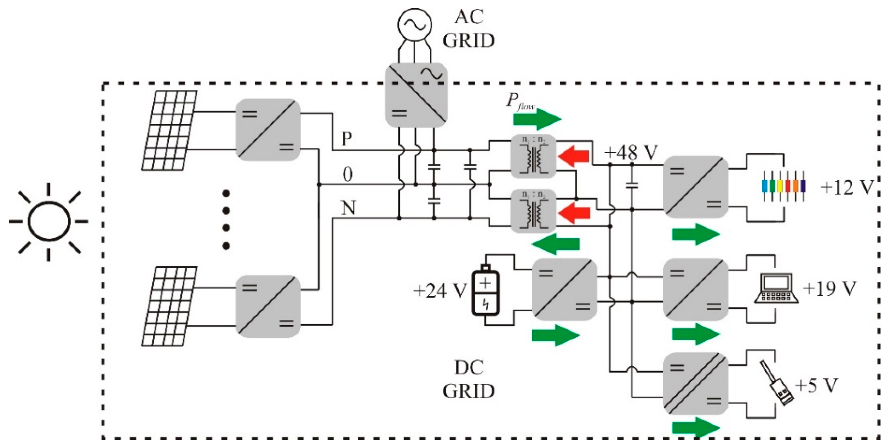
A DC picogrid, based on state-of-the-art architectures [3,6,16], is depicted in Figure 1, which emulates a building and/or residence with a DC grid implementation. In this grid, a bipolar DC network is realized (P0N poles), which has the possibility of injecting the energy generated by the panels in the AC grid or, alternatively, directly supply DC loads bypassing the DC–AC–DC transformation.
A lot of effort has been spent to propose new topologies and systems to interconnect PV generation in AC or DC grids with, respectively, microinverters [17,18,19] and microconverters (DC power optimizers) [20,21,22,23,24] which, in essence, are step-up converters since the PV panel output voltage is lower than the AC grid or DC bus voltages. The control aspects of this system and MPPT strategies are common subjects in the literature [20,25,26,27].
Different strategies to step-up the voltage have been studied and proposed in the literature, such as: isolated step-up topologies [17,21,28], coupled-inductor, nonisolated topologies [29,30,31,32,33,34,35], nonisolated topologies with Capacitor–Diode/switch structure [19,36,37,38], nonisolated topologies with Inductor–Diode/switch [39,40] and nonisolated topologies with Capacitor–Diode/switch and Inductor–Diode/switch structures [41,42]. These structures are known, respectively, as switched-capacitors and switched-inductors. An adaptation of the Inductor–Diode structure is proposed in [
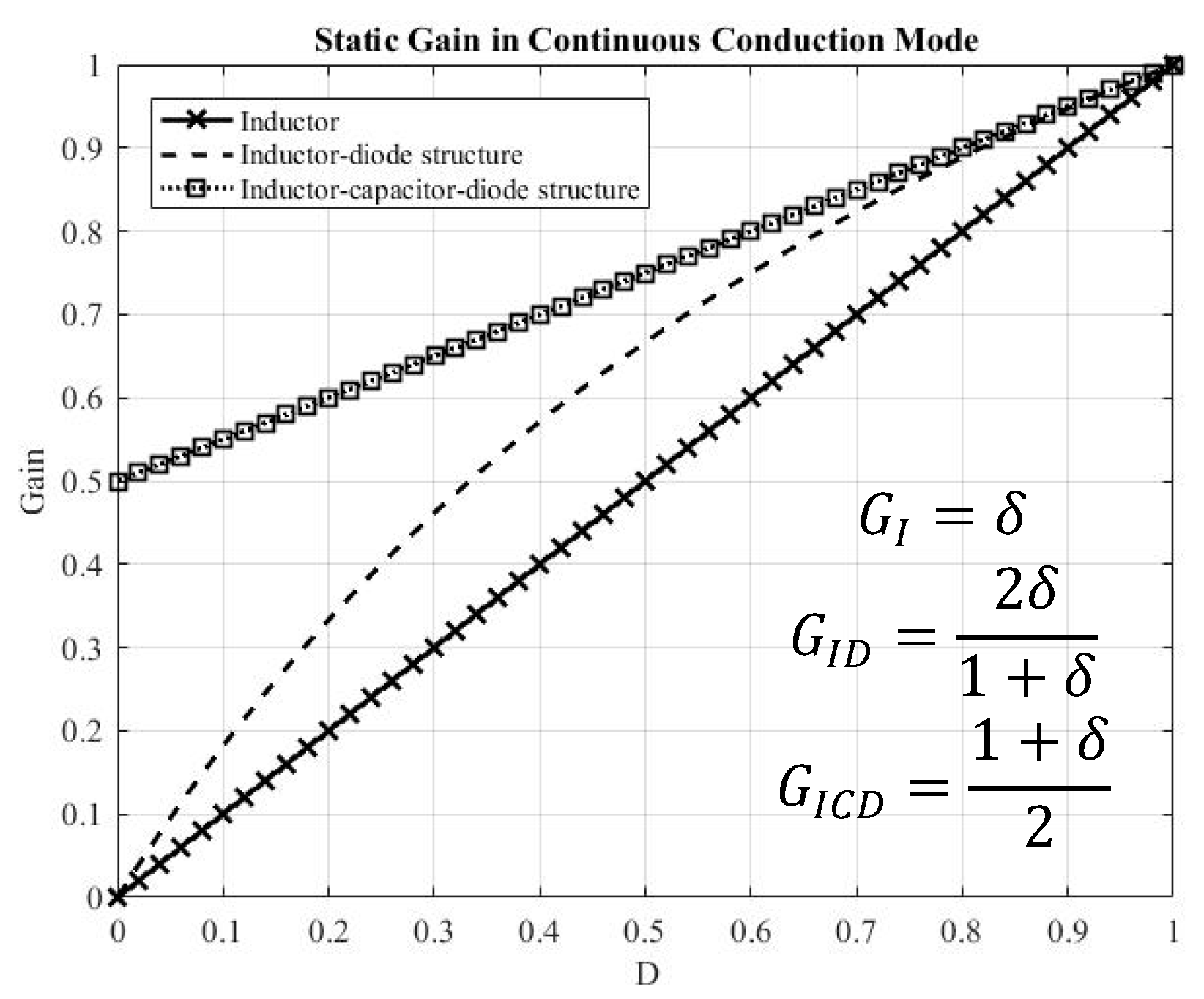
43], where a capacitor replaces one diode and changes the gain of the structure for step-up applications. Each of the above-mentioned strategies to step-up voltages has its advantages and disadvantages. For instance, isolated topologies and coupled inductor topologies have the flexibility of, based on the turns ratio of the magnetic device, select the suitable output voltage requirement, although it is known that these magnetic components are, together with heatsinks, the bulkiest components in a converter. Switched capacitor and switched inductors do not bring this flexibility once the gain is defined based on the operational duty cycle of the active switches. Inductors are more reliable components than capacitors, giving an advantage in terms of reliability, while capacitors are more compact and more suited for high power density applications.
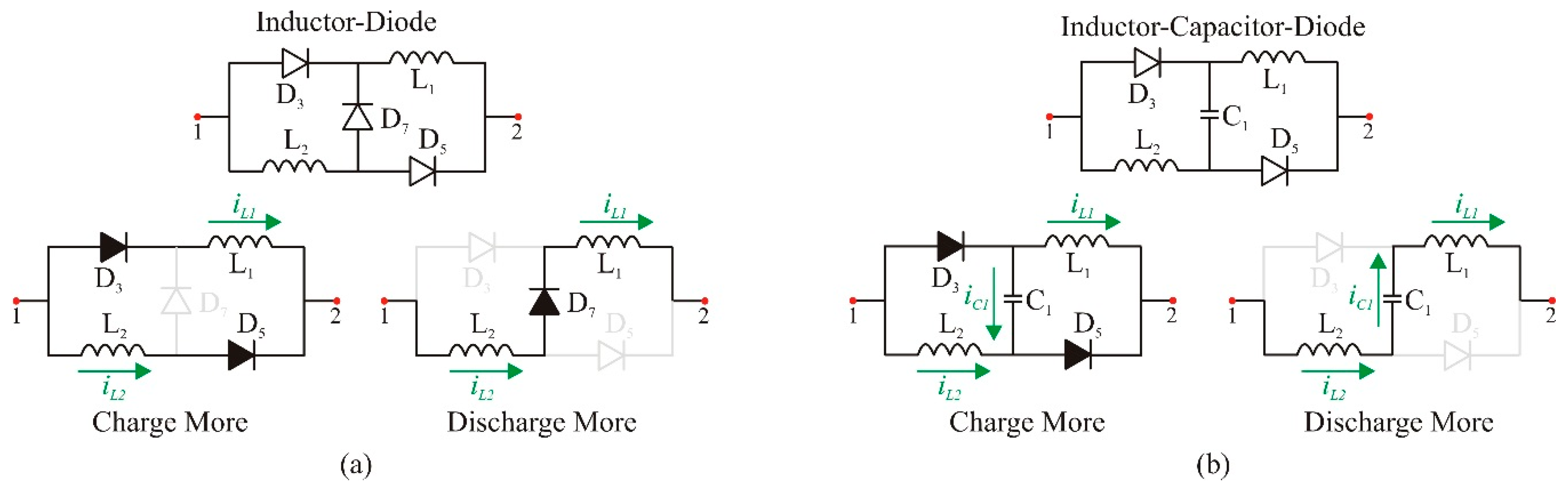
In step-down conversion ratio converters, the Capacitor–Diode/switch structures are commonly used to improve the step-down ratio of the converters [44,45,46]. On the other hand, the implementation of an Inductor–Diode/switch and Inductor–Capacitor–Diode structures in the step-down conversion ratio is not extensively discussed in the literature, with few exceptions that explore both step-up and step-down structures [
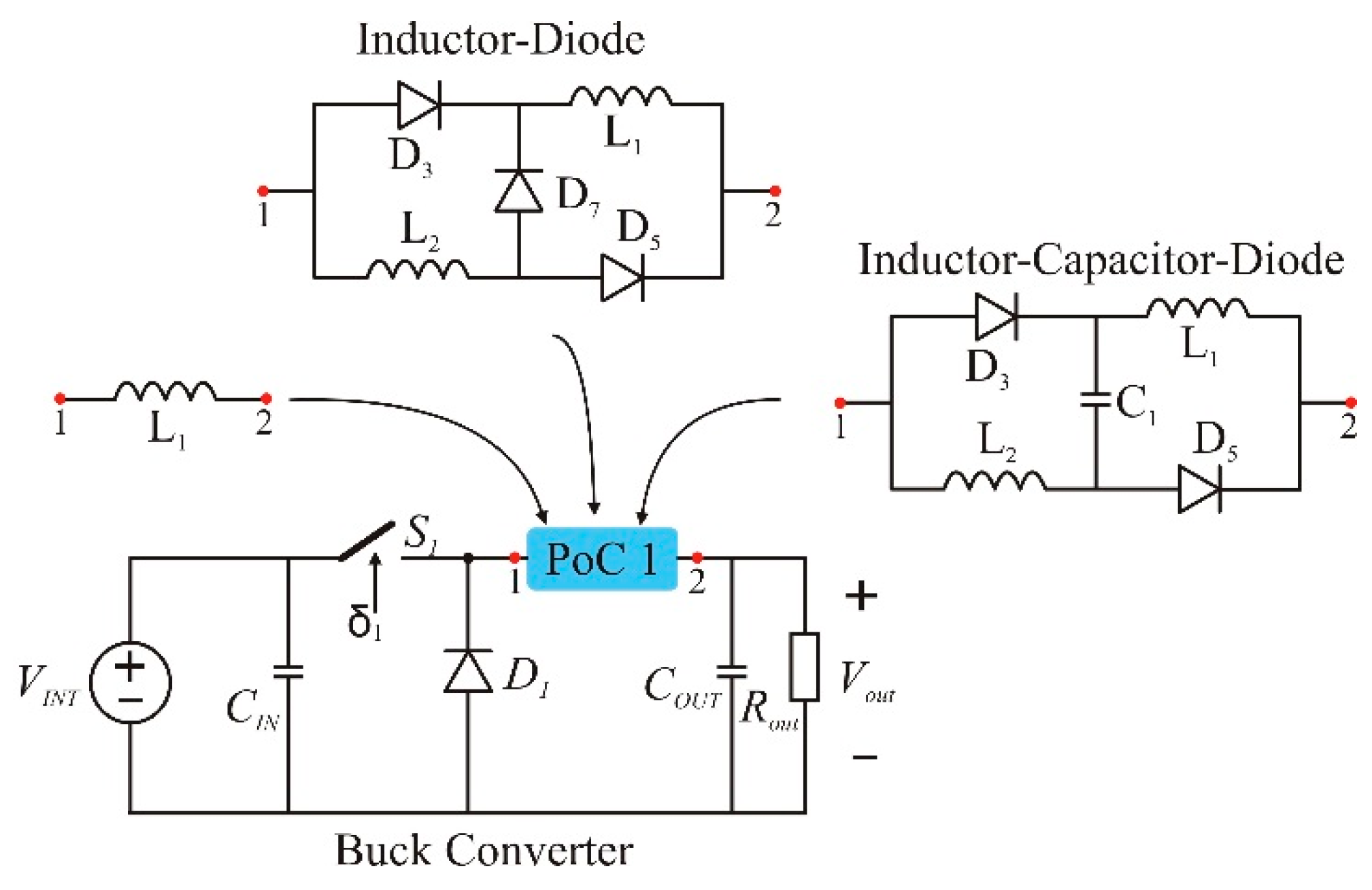
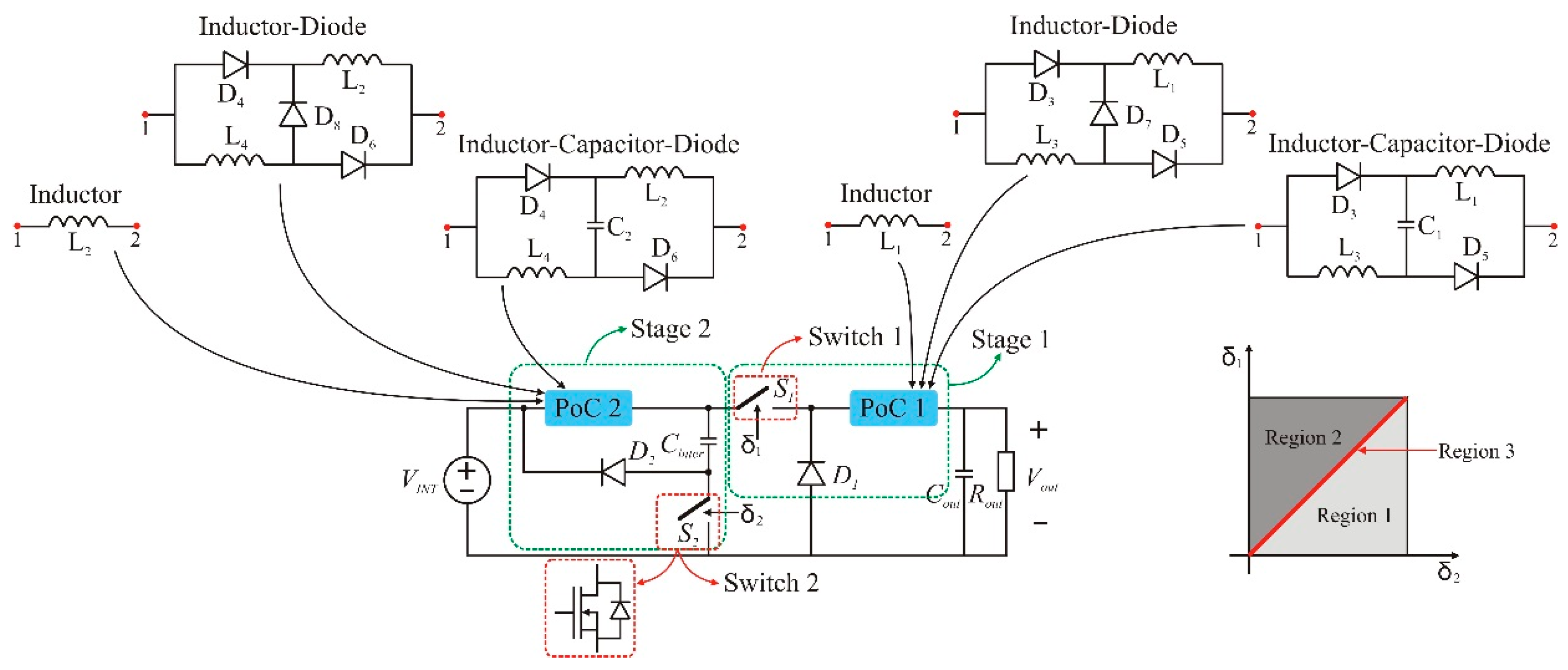
39]. The structures evaluated in this paper are shown in Figure 2. The Inductor–Diode structure shown in Figure 2 can offer a redundant path if one diode of the structure fails in open-circuit, as proposed in [47]. In steady-state, the inductors can be considered as current sources and, due to the structure operability discussed in Section 4, mitigate the implementation of current sensors for control purposes, since the current balance between the inductors is naturally achieved without any control strategy (switched-inductor characteristic). The only sensor that might be consider for implementation is a voltage sensor, if the application requires a regulated and constant output voltage level for the entire load range of operation. For instance, a contraction technique was proposed to control a regular step-down converter [48].
With these considerations, the objective of this paper is to investigate the influence of the Inductor–Diode (ID) and Inductor–Capacitor–Diode (ICD) structures in the step-down conversion stage from 48 V to 12 V input-to-output voltage. The main contributions of this paper are (1) an analysis of the influence of the ID and ICD structures in a step-down conversion system; (2) the presentation of a full theoretical analysis of the converters generated; (3) applying the ID and ICD structures in a quadratic buck converter; (4) analyzing the intermediate voltage level behavior for different operational points, showing the intermediate voltage flexibility of the circuit, which is beneficial for a voltage regulation point of view; (5) creating a flexible test bench to be able to validate the proposed converters and; (6) experimentally validatation with waveforms of the topologies studied in the paper.
The paper is organized as follows; Section 2 presents the analysis of the ID and ICD structure in a regular single-stage buck converter and its impact on the gain of the converter. Section 3 presents the two-stage buck converter, known as quadratic buck converter [49], to enable the converter applying the ID and ICD structures to achieve the required output voltage levels. The operational principle of the topologies generated by the proposed intra-exchangeability is explained in Section 4. Section 5 explores the simulation results of the proposed topologies, showing the intermediate and output voltage levels that are obtained for each possible configuration. Section 6 describes the experimental test bench built for further validation, showing experimental waveforms that validate the theoretical analysis presented in Section 3 and Section 4. Section 7 presents the main conclusions and future work suggestions.

2. Impact of Inductor–Diode and Inductor–Capacitor–Diode Structures in a Step-Down Converter

This section has the objective of investigating the influence of the ID and ICD structure in a step-down buck converter. Inductor I, shown in Figure 3, is replaced by ID and ICD structures and the PWM modes are described herein. The main difference between the ID and ICD structures is that the capacitor of the ICD is also charged during the magnetization of the inductors. When discharging, the capacitor also discharges, providing energy to the load. The capacitor stores part of the energy that is delivered to the load, which helps decrease the size of the inductors, since less energy is stored in their magnetic field. Additionally, the capacitor changes the voltage applied across the inductors during demagnetization, which changes the gain of the structures, as described herein.

2.1. PWM Mode 1

In this PWM mode, the switch S1 commutates from ‘open’ to ‘close’, changing the equivalent circuit of the converter. The equivalent circuit for this mode is shown in Figure 4a,b for the ID and ICD applications in PoC1, respectively. During this mode, the voltage applied in the inductor terminals VL1 and VL2 is positive, due to the step-down mechanism, and energy is magnetically stored in the inductors during the process. The voltage applied across the inductors terminals has the same level (internally in ID and ICD structures), which leads to similar current level in the inductors of the structures. In the ID structure, the inductors store energy during this PWM Mode while in the ICD structure the inductors and the capacitor of the structure store energy.

2.2. PWM Mode 2

In this PWM mode, the switch S1 commutates from ‘close’ to ‘open’. The equivalent circuit for this mode is shown in Figure 4c,d for the ID and ICD structures, respectively. During this PWM mode, the voltage applied across the inductors terminals VL1 and VL2 is negative, since diode D1 is forward biased, leading to a demagnetization of these inductors. The current across both inductors is equal as these components are in series, which guarantees the same negative voltage level across the inductors of the structures during the demagnetization. The demagnetization mechanism for both structures is similar, since in both structures the inductors are connected in series and the same current flows through the passive components.
From the above PWM mode analysis, the theoretical voltage profile for all the inductors in both structures are presented in (1). These equations are applied in (2) to obtain the conversion gain of the structures, in steady-state.
I D I C D { V L 1 = V L 2 = V I N V O U T     d u r i n g     δ 1 V L 1 = V L 2 = V O U T 2     d u r i n g     ( 1 δ 1 )     { V L 1 = V L 2 = V C 1 = V I N V O U T     d u r i n g     δ 1 V L 1 = V L 2 = V I N 2 V O U T     d u r i n g     ( 1 δ 1 )
V L ¯ = 0 T S v L d t = 0

2.3. Theoretical Gain in Continuous Conduction Mode

To obtain the theoretical voltage gain profile of the topologies, operation in steady-state is considered, which allows the application of (1) in (2) to obtain the ideal gain of the structures. After some mathematical manipulation, the theoretical expression that represents the gain of the Inductor–Diode (ID) and Inductor–Capacitor–Diode (ICD) structures, respectively, is graphically represented in Figure 5. From Figure 5, it is noticed that the operational voltage range tackled in this paper cannot be realized with the ICD structure, since its gain range is, ideally, between [0.5 ; 1]. To overcome this, the quadratic buck converter—a nonlinear step-down converter generated by two buck converters connected in series with each other—as depicted in Figure 6, is the base topology used to generate the converters proposed in this paper. This converter presents an intermediate stage, giving an extra degree of freedom for implementation, since two voltage levels are generated in the same converter and both can be used to supply loads.
Only one switch is implemented on the power stage of the conventional quadratic buck, which has the benefit of control strategy simplification; and the intermediate voltage level is in the function of the duty cycle applied to switch S1. If a second switch is introduced in the power stage, the degree of freedom for voltage regulation in the intermediate stage is guaranteed by the duty cycle of the second switch S2, although the control strategy might increase in complexity, if applicable. Since the objective of the topologies is to improve the flexibility of the conversion ratio and the overall system, the quadratic buck with two switches is the converter that will be extensively explored in the next section, together with the intra-exchangeable PoC structures presented in Figure 3.

3. Double-Switch Two-Stage Quadratic Buck Converter for Voltage Regulation

As previously mentioned, the two-stage buck converter, most known as quadratic buck converter, is the base topology used for the intra-exchangeable methodology used herein for testing multiple configurations, based on the ID and ICD structures, applied for voltage regulation. Since a second stage is now implemented in the power circuit, the intra-exchangeability increases the amount of topologies that can be generated. More specifically, with three structures and two stages, the number of topologies generated is 32 = 9, where only the conventional quadratic buck is already explored in the literature. Figure 6 exemplifies the possible configurations that can be obtained from the proposed intra-exchangeability between a regular inductor (I) and the ID and ICD structures. When an I structure is connected to PoC1 and PoC2, the regular quadratic buck is obtained. In total, nine topologies are generated from this method and, since two switches are implemented in the power stage with independent duty cycles, three regions of operation can be explored and will be briefly discussed herein. The regions of operation are highlighted in Figure 6, named as region 1, when duty cycle δ2 is higher than duty cycle δ1; region 2, when δ1 is higher than δ2; and region 3, when both duty cycles are equal. The switch realization is based on a MOSFET with an antiparallel diode, as shown in Figure 6.

3.1. Region 1 (δ2 > δ1)

Operating in Region 1, the two stages of the quadratic buck structure operate independently, leading to intermediate and output voltages, depending on the duty cycles δ2 and δ1. The intermediate voltage across capacitor Cinter depends on the structure connected in PoC2 and the duty cycle δ2 to command switch S2. The output voltage, on the other hand, depends on both structures connected in PoC2 and PoC1, since the intermediate voltage level is the input voltage of the first stage. The equations presented in Figure 5 are reused to find the intermediate and output voltages generated by this integration. Table 1 summarize the analysis, showing the theoretical gain profile of the intermediate stage and output stage in function of the input voltage of the circuit and the duty cycle of switches S1 and S2. For instance, if the ID structure is applied in PoC1 and the I structure in PoC2, the intermediate and output voltages of the circuit are, respectively, related to equations δ 2 and δ 2 2 δ 1 1 + δ 1 , , which means that the intermediate voltage is regulated by the nominal set point of the duty cycle applied in S2 and the output voltage depends on the duty cycles applied to S1 and S2. The analysis considers that the duty cycles are independent, and with no phase-shift between each other.

3.2. Region 2 (δ2 < δ1)

Operating in this region, the second stage of the quadratic buck depends on the first stage, since the duty cycle of switch S1 is higher than the duty cycle of switch S2. Consequently, the intermediate capacitor continues to discharge even if the switch S2 is in ‘off’-state (due to the antiparallel diode between drain-source points of S2). In this operational region, the duty cycle δ1 defines the intermediate voltage level and the output voltage level. Table 2 summarizes the voltage levels in this region of operation.

3.3. Region 3 (δ2 = δ1 = δ)

Region 3 is the region when both switches operate with the same duty cycle (δ2 = δ1 = δ) and the duty cycles are in phase with each other. For this case, the intermediate and output voltages are subject to the operational duty cycle of the circuit. The theoretical analysis, shown in Section 4, is related to operation in Region 3. Table 3 summarize the voltage gain of the topologies generated by this intra-exchangeability.
Although nine different topologies are realized in this analysis, only six different output voltage profiles are obtained, since the topologies I-ID/ID-I, I-ICD/ICD-I and ID-ICD/ICD-ID provide the same output voltage profile, while different intermediate voltage profiles are observed. Figure 7 shows the graphical representation of the output voltage profiles presented in Table 3. It is noticed that, due to the equations of the voltage profile shown in Figure 5, the highly nonlinear behavior of the quadratic buck converter is attenuated when the ID or ICD structures are used in one of the PoCs. The gain of the topologies, mathematically expressed in Table 3 and graphically in Figure 7, is less nonlinear if compared with the conventional quadratic converter, which is interesting for control purposes. These converters, however, are not suitable for applications that require high step-down capability, since the ID and ICD structures decrease the step-down capability of the structure, as shown in Figure 5 for application in a regular buck and Figure 7 in the quadratic version. Although the component part count increases for ID and ICD implementation, it also increases the flexibility to achieve multiple intermediate voltage levels to supply different loads.
On comparison of Table 2, related to region 2, and Table 3, related to region 3, it is noticed that the gain of the structures are the same. As mentioned in the previous subsection, this behavior occurs because the antiparallel diode of switch S2 continue to conduct even if switch S2 is in ‘off’-state until switch S1 commutates from ‘close’ to ‘open’. This analysis concludes that operational regions 2 and 3 generate similar PWM modes and, consequently, the same intermediate and output voltage levels while region 1 is distinguished by the independence between the stages. Section 4 will further discuss the operational principle of the double switch quadratic buck with ID and ICD structures, for operation in Region 3.

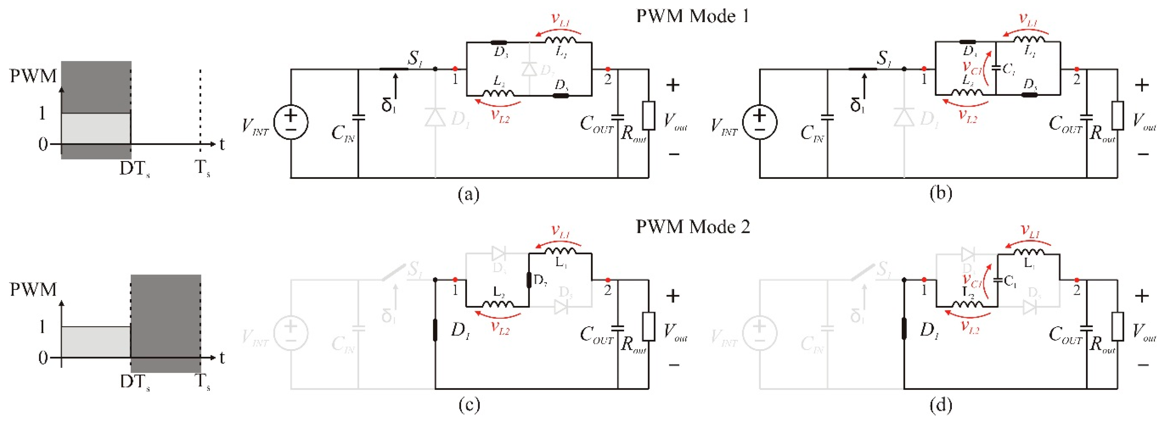
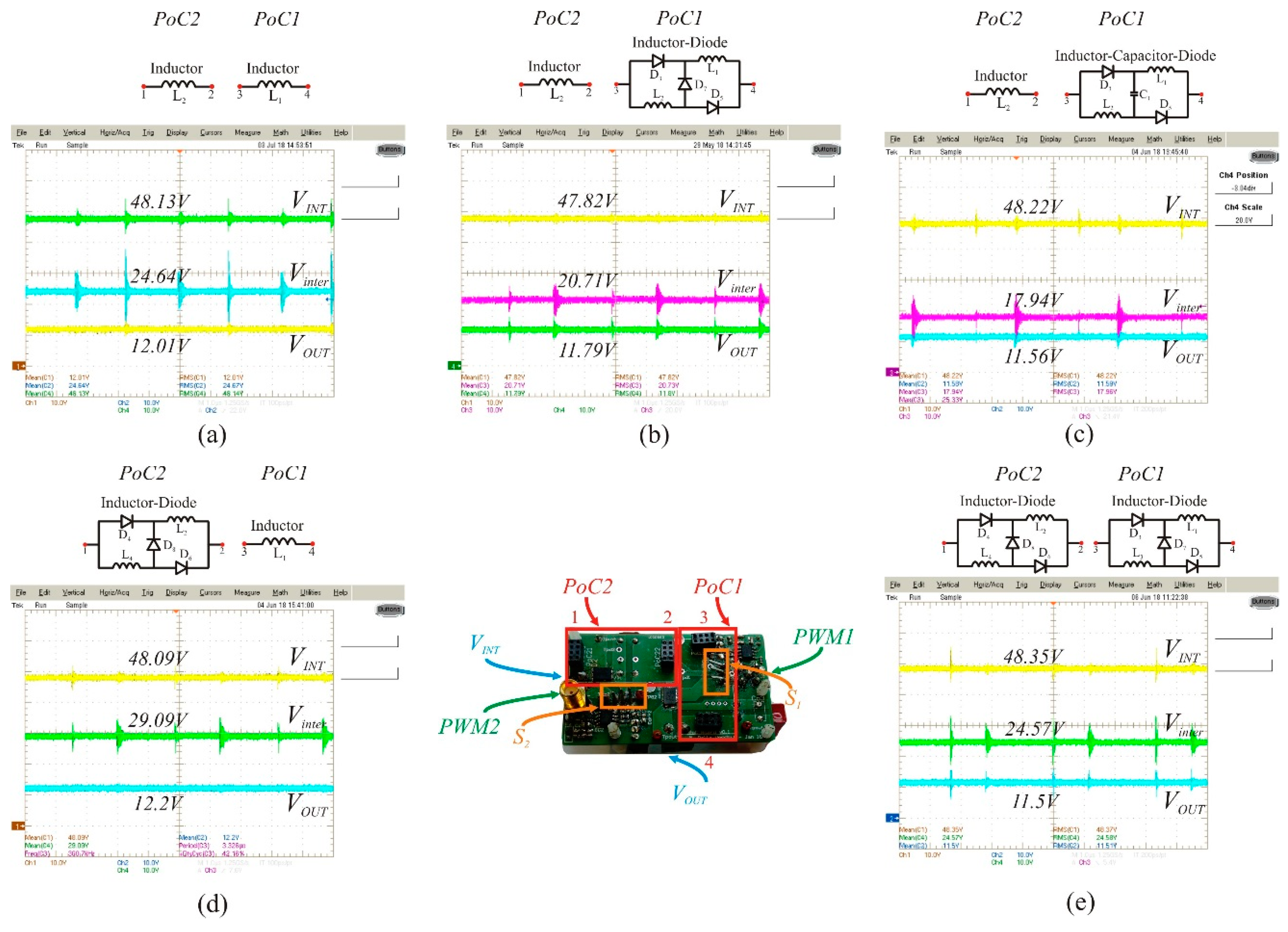
4. Operational Principle of the Double Switch Quadratic Buck Converter in Region 3

Similar to Section 2, where the one-stage I, ID, and ICD topologies have been introduced, this section introduces the PWM modes of the two-stage I, ID, and ICD topologies, where the PWM signal remains the same. The phase shift between δ2 and δ1 is considered zero (in phase with each other) for the specific analysis but if differs from zero, the gain behavior shown in Table 1, Table 2 and 
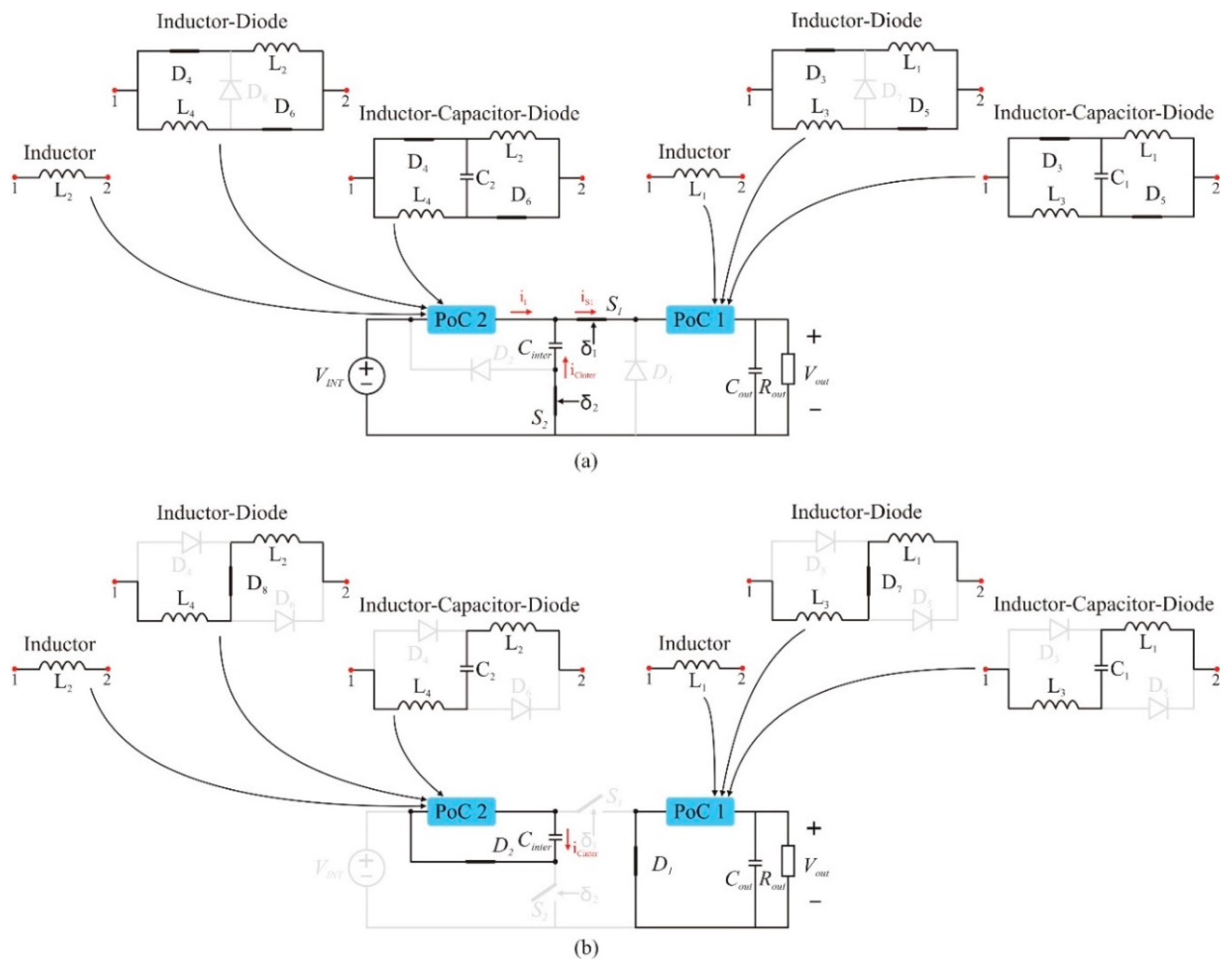
Table 3 will differ, since the phase-shift will influence the PWM stages and, consequently, the gain of the structures. The equivalent circuit for the first and second stages, considering all the possibilities between the exchangeable circuits, are present in Figure 8a,b, respectively. In order to evaluate the main characteristics of the topologies, the equivalent circuits presented in Figure 8 are used to mathematically evaluate the voltage and current stresses in all power components. This information is crucial to further dimension the components for practical implementation.
The voltage stress across each power semiconductor are extracted from the PWM mode stages in Figure 8 and summarized in Table 4. The voltage stress across switch S1 and diode D1 is affected by the structure applied in PoC2, for instance, if the I structure is applied to PoC2, the voltage stress across switch S1 is defined by ( 1 + δ ) V I N , while if the ID structure is applied in PoC2, the voltage stress across switch S1 is defined by equation ( 1 + 3 δ ) ( 1 + δ ) V I N . Similarly, the voltage stress across diodes D3/D5/D7, connected to PoC1, are related to the structure connected in PoC1. For instance, maintaining PoC2 fixed with the ID structure, if the ID structure is connected to PoC1, the voltage across the diodes D3/D5 is expressed by δ 2 ( 1 + δ ) 2 V I N and, if PoC1 is changed for an ICD structure, the voltage across diodes D3/D5 is expressed by δ ( 1 + δ ) V I N . Switch S2 and diode D2 stresses are independent on the structures and are equal to the input voltage VIN. The voltage stress across diodes D3-D4-D5-D6-D7-D8, which are the diodes implemented in the ID and ICD structures, are related to the operational duty cycle, input voltage, and in which PoC the structures are implemented.
Similarly, the PWM modes also provide the RMS current stress in each power semiconductor. To evaluate the RMS current stress in all components, equation (3) is introduced, where ix1 is the current that the semiconductor conducts during the first PWM mode and ix2 is the current conducted during the second PWM mode. Applying (3), the current stress in each semiconductor is characterized and presented in Table 5. Different than the voltage stress, the current stress of switches S2 and D2 depend on the structure connected to PoC2 but are independent of the structure connected to PoC1. For instance, the RMS current stress across switch S2 is expressed by I I N ( 1 δ ) δ 1 δ if the I structure is connected to PoC2, and expressed by I I N ( 1 δ ) 2 δ 1 δ if the ID structure is connected. It is also noticed that the current is independent on PoC1, in this case.
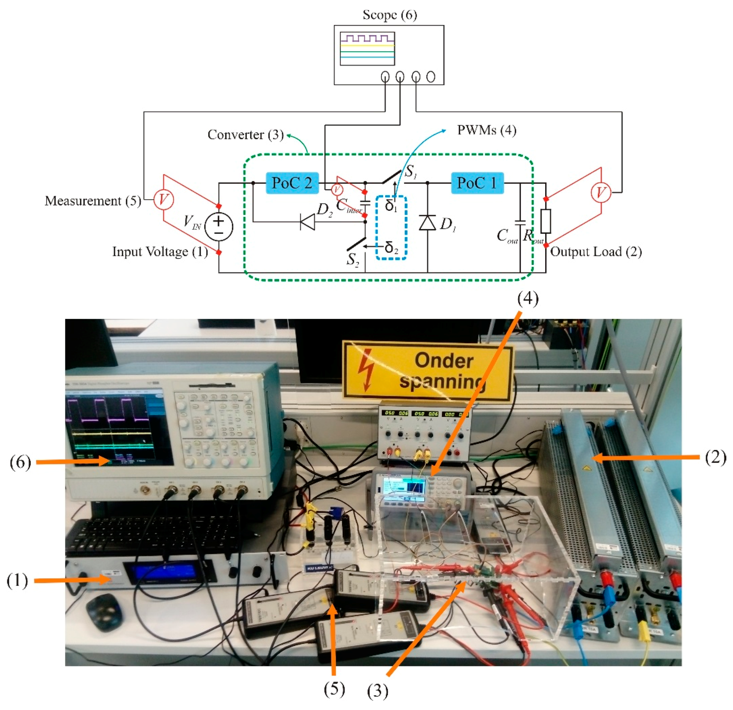
The analysis abovementioned is important in order to select the components for experimental validation, since the RMS current and voltage stress are the most important characteristics to select MOSFETs and diodes. The next section presents a numerical simulation for the proposed converter performed in PLECS (4.0.2, Plexim GmbH, Zurich, Switzerland).
i x R M S = 1 T S ( 0 D T S i x 1 2 d t + D T S T S i x 2 2 d t )

5. Numerical Simulations

A numerical simulation was carried out to show the available intermediate voltage levels when an output voltage of 12 V is set as standard output voltage. The 12 V voltage level can supply low voltage/low power loads to, for instance, LEDs or to charge small batteries (unidirectional power flow to charge, since the topologies are unidirectional); this is one of the main reasons to fix the output voltage on this level. The simulation and experimental parameters are presented in Table 6.
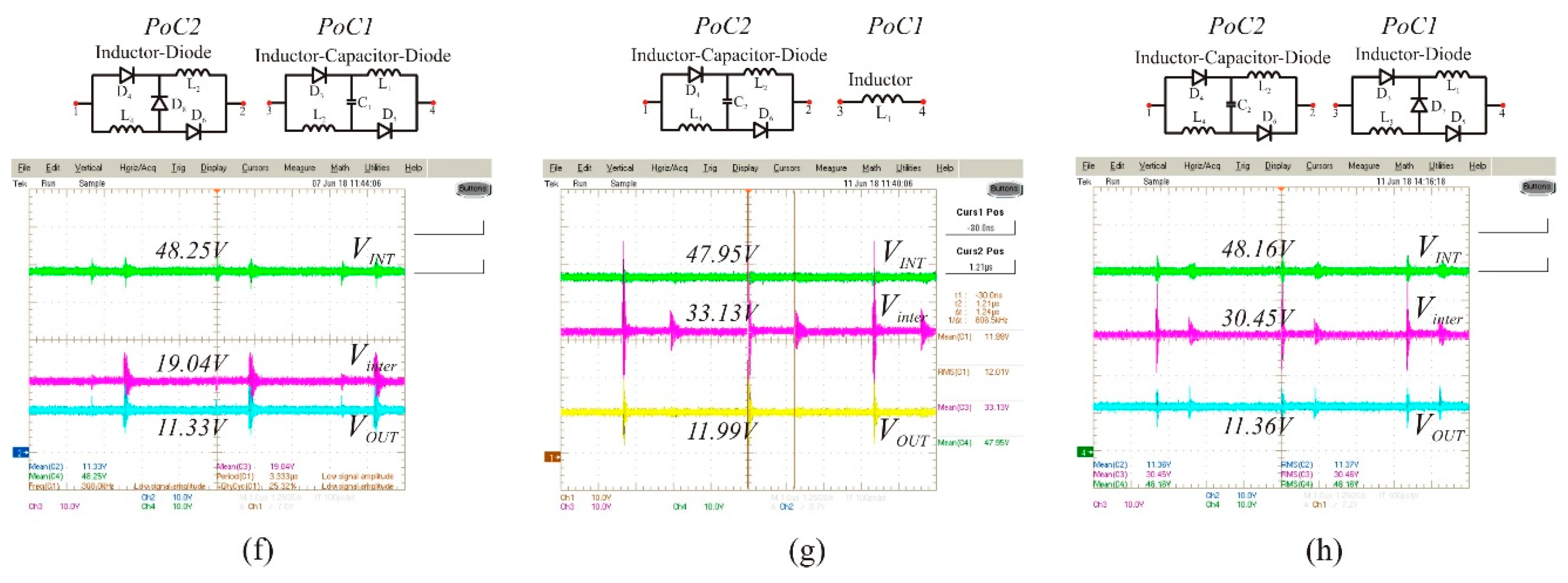
Different intermediate voltage levels are generated, depending on the structure connected in PoC2 and the operational duty cycle of the converter, as shown in Table 3. The simulation model was develop in PLECS. The only configuration that is not able to be simulated and experimentally validated in this paper is the ICD-ICD structure, since the input/output voltage level is 48 V/12 V and the theoretical gain of this structure is 0.25 < ICD-ICD < 1, making it impossible to provide the required output voltage.
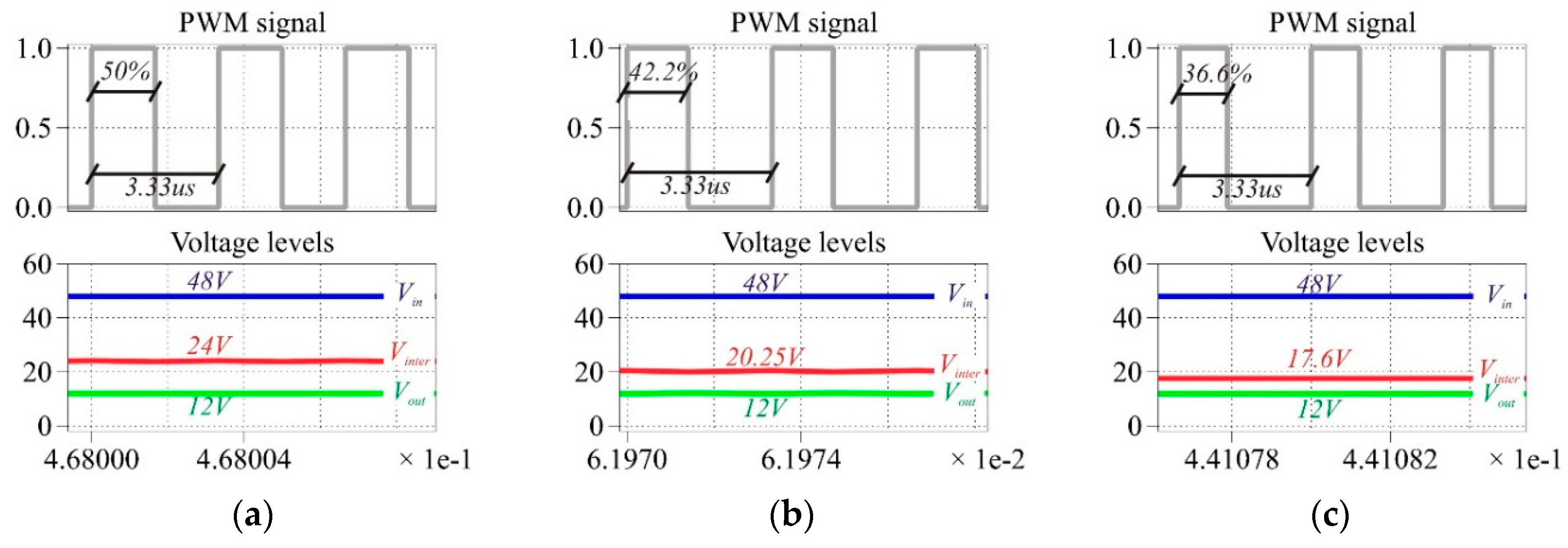
A simulation is performed for each configuration and the results are shown in Figure 9. The conventional quadratic buck with I-I is show in Figure 9a, generating an intermediate voltage level of 24 V. According to Table 3, the I-ID and ID-I configurations generates the same output voltage but different intermediate voltage levels for operation with the same duty cycle. This behavior is proved via simulation and presented in Figure 9b,d, where the voltage level of 20.25 V (I-ID) and 28.5 V (ID-I) are obtained for a duty cycle of 42.2%.
Similarly, the topologies I-ICD and ICD-I operate with the same duty cycle (36.6%) and input/output voltages, however the intermediate voltage level changes since is applied different structures in PoC2. Simulation results shown in Figure 9c,g confirm the analysis, since an intermediate voltage of 17.6 V (I-ICD) and 32.8 V (ICD-I) are obtained and available to supply loads in different voltage ranges in a flexible way. The structures ID-ICD and ICD-ID are also evaluate via simulation for similar input/output voltages. Intermediate voltages of 19.2 V (ID-ICD) and 30 V (ICD-ID) are obtained and shown in Figure 9f,h, respectively, validating the theoretical analysis presented in Table 3. Additionally, the last configurations present similar overall gain (δ) with the regular buck converter, however they present an additional voltage level that can be used to supply additional loads in different voltage levels. The drawback of the structure, compared with the conventional buck, is the component part count, since the number of inductors and diodes in the power stage increase.
Finally, the ID–ID structure is briefly discussed herein. Figure 9e shows the voltage levels obtained from simulation. Similarly with the conventional I-I quadratic buck, an intermediate voltage level of 24 V is obtained, however an operational duty cycle of 33.3% is used to match the desired output voltage of 12 V.
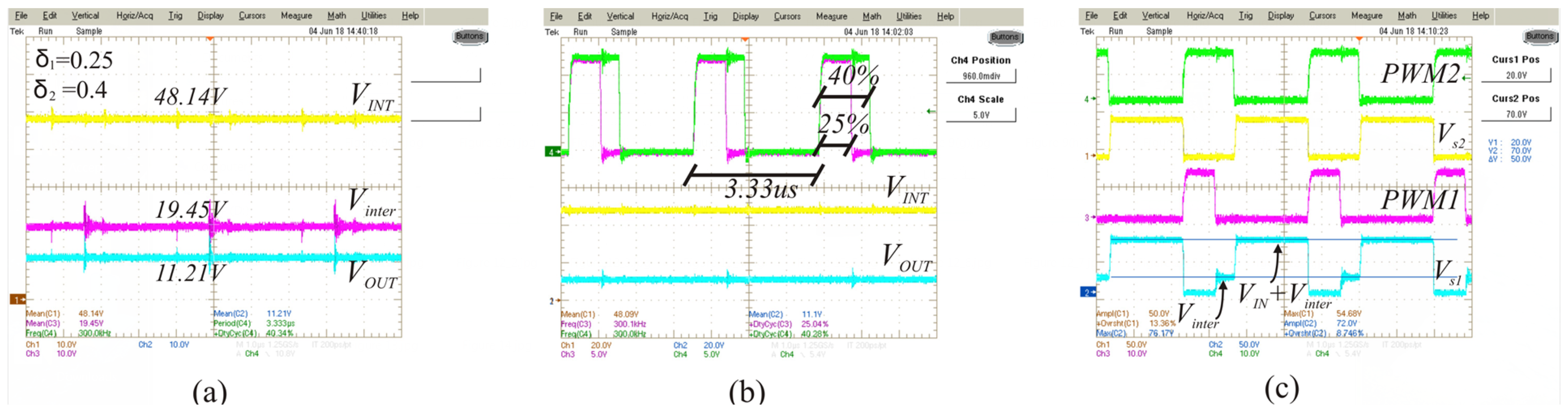
The simulations were performed with a switching frequency of 300 kHz (switching period of 3.33 µs), since this frequency was used to calculate the I, ID, and ICD inductances for further implementation of the structures. All the inductances were select to present a 20% ripple current limit across the inductors in nominal power. A summary of the theoretical inductor current expressions in each scenario is present in Table 7, in function of the input current IIN. From the PWM mode stages discussed in the previous section and shown in Figure 8a,b, the inductors of the ID and ICD structures charge its terminals in parallel and discharge in series, which guarantees natural balance between the internal currents of the structure. This characteristic enable the non-use of current sensors to control the inductor current, since this control is guarantee directly by the ID and ICD structures, also known as switched-inductor structures. The drawback, as previously mentioned, is the increase in the number of components in the power stage.
With the objective of validating the equations shown in Table 7, a comparison between the theoretical analysis and numerical simulation results was performed and shown in Table 8. The input/output voltage of the circuit is 48 V/12 V and a rated input power of 100 W. The different configurations operate with their respective duty cycles to generate an output voltage of 12 V (check Figure 7 for duty cycle). The comparison shows that the theoretical equations match the simulation results, which proves the validity of the equations to select the correct inductances for experimental verification.

6. Experimental Verification and Test Bench

6.1. Region 2 (δ2 < δ1)/Region 3 (δ2 = δ1 = δ)

This subsection will discuss the results obtained for operation in Region 3 (δ2 = δ1 = δ). The topologies, discussed in Section 3 and Section 4, were realized for further validation. A test bench was built for experimental verification of the configurations discussed herein. Figure 10 shows the test bench setup, together with a simplified bench schematic. It is shown in Figure 10 that a function generator (equipment (4)) is used to generate the PWM signals to drive S1 and S2. The experimental results shown herein are in open-loop operation, without a control strategy to regulate the intermediate and output voltage levels. Figure 11 shows the converter realization (middle) surrounded by the PoCs (PoC2 and PoC1) developed for each configuration (the inductors were selected based on the 20% maximal current ripple for each structure).
The PoCs, developed to test the different configurations, were designed separately following the plug-n-play methodology. As shown in the converter realization in Figure 11, the PoC2 and PoC1 are actual points of connection, where different external boards are connected to test different inductor configurations (I, ID, and/or ICD). Points 1 and 2, for PoC2, and 3 and 4, for PoC1, are available to connect the external PoCs. Additionally, Table 6 present the parameters defined for the experimental setup, in which the switching frequency of 300 kHz was select to simulate and experimental validation.
When comparing the waveforms presented in Figure 9a–h (simulation) and in Figure 12a–h (experimental), it can be seen that the voltage levels in all topologies are similar in shape (DC shape) and in amplitude. Figure 9 and Figure 12 present the input, intermediate, and output voltages of the converter for the following configurations (PoC2-PoC1); (a) I-I, (b) I-ID, (c) I-ICD, (d) ID-I, (e) ID–ID, (f) ID-ICD, (g) ICD-I, and (h) ICD-ID. Small deviations are observed between the amplitude values in simulation and in the experimental waveforms due to the nonidealities inherent in the components selected to build the prototype. We also noticed that spikes of voltage appears in all voltage levels. This behavior is common in circuits that operate in high frequency, since internal parasitics of the components and also the parasitic inductances related to tracks and soldering points start to become prominent. Additionally, the commutation between ‘on’- and ‘off’-stages of switches S1 and S2 also generate internal oscillations in the circuit.
As mentioned in Section 3, the gain analysis performed for the operation in region 2 and 3 results in the same gain expressions. The experimental results shown herein are for operation in region 3, but can be extended for the case when region 2 is in operation.
As discussed previously, is was shown that for different operating points and configurations connected in PoC2 and PoC1, different intermediate voltage levels are obtained for an input/output voltage of 48 V/12 V. This voltage, which varies from 33 V to 18 V depending the configuration, is available in the intermediate stage and can be used to supply loads in a broad range. Depending the required intermediate voltage, the best suited configuration can be selected to connect in PoC2 and PoC1. The ICD structure, as shown in Figure 5, limits the gain in the region between [0.5 ; 1], and can be used for a small voltage regulations with a certain accuracy. The ID structure, on the other hand, presents a nonlinear gain behavior in the range between [0 ; 1]. For the same duty cycle, this structure can be used to achieve gains in between the regular buck with I structure and the buck with ICD structure, with the disadvantage of a nonlinear gain.

6.2. Region 1 (δ2 > δ1)

For operation in region 1, an extra PWM mode is performed between the normal PWM modes 1 and 2, during the switching period. This extra PWM mode guarantee the independence between stages 1 and 2, leading to the gain presented in Table 1 for all possible PoC configurations. We noticed that the intermediate gain depends only on the duty cycle δ2, while the output gain is relate to duty cycles of both stages, since the converters are cascade connected.
Figure 13 shows the PWM modes for operation in region 1 for the I-ICD configuration. Nevertheless, this analysis can be extended for all configurations. As previously mentioned, an extra PWM mode arises during the switching period (PWM mode 2 in this analysis). Switch S1—the component which is subject to the greatest voltage stress among the power components—as highlighted in Table 4, blocks only the intermediate voltage level during the switch transient between ‘on’ and ‘off’ while when operates in regions 2 and 3, the switch blocks the sum between the intermediate voltage and the input voltage. This phenomenon enables the reduction of switching losses in this component once the voltage that the component blocks during the switching transient has a lower value compared with the normal operation, although the maximum voltage that the switch needs to block remains in the same level as shown in Table 4.
Figure 14 presents an experimental verification of the stages discussed previously and shown in Figure 13. Figure 14a presents a waveform with the significant voltage levels of the circuit. As expected, an intermediate voltage of 19.5 V is achieved for a duty cycle of 40% applying the I structure in PoC2. Additionally, Figure 14a also presents the second voltage regulation stage made by the ICD structure connected in PoC1, operating with a duty cycle of 25%, in which a voltage of 11.2 V is achieved at the output of the converter. Figure 14b presents the PWMs applied to the circuit and its switching period, together with the input/output voltage of the circuit. As expected, input and output voltages are in accordance with the theoretical analysis above presented.
Finally, Figure 14c shows the experimental results of the voltage stress across the active semiconductors S1 and S2. For the same duty cycle abovementioned, the voltage stress across switch S2 is independent of the operational duty cycle and equal to the input voltage, as shown in Figure 14c. Additionally, the stress across switch S1 was also evaluated and presented in Figure 14c. It is verified that, as theoretically explained, the voltage that the switch blocks during transition between ‘on’ and ‘off’ stages is the intermediate voltage across Cinter, although the maximum voltage stress is related to the sum of input and intermediate voltages (verify PWM mode 3 between points 2–3 in Figure 13). Moreover, the switching losses generated by the overlap between current and voltage during the transition time decrease due to the lower blocking voltage during this transition. For operation in region 1, the addition of switch S2 with independent duty cycle improves the flexibility of the system and decreases the switching losses across switch S1.
As discussed previously, the introduction of the ID and ICD structures in a step-down configuration (one-stage buck or quadratic buck) enable the possibility to change the voltage level of these structures. When applied in a one-stage buck converter, the ICD structure present similar voltage gain ( 1 + D 2 ) as the converter proposed in [50]. The structures, however, present different functionalities, since the abovementioned structure is a switched capacitor based converter with one switch, three diodes, one inductor, and three capacitors in the power stage while the structure, herein presented, is a switched inductor based topology with one switch, three diodes, two inductors, and one capacitor in the power stage. In terms of component part count number, the one-stage ICD structure present lower amount of components compared with the switched capacitor version that present similar gain [50]. The ID structure, on the other hand, presents a nonlinear step-down behavior with one extra diode and one less capacitor in the power stage (compared with the above-mentioned converters).
The ID structure is also explored in step-up configurations [39] and, when applied in a step-down structure, it changes the structure to a one composed by two inductors and two diodes, which leads to a gain of D 1 + D , performing a higher step-down ratio them the ID structure. A topology with different switched capacitor/inductor structure is proposed for similar voltage gains [44] Comparing these topologies with the quadratic-buck configuration applying the ID and I structures (see Table 3), the gain of these structures is 2 D D 1 + D . The proposed structures, although implement more components in the power stage, present a higher step-down ratio for duty cycles lower than 0.5. For duty cycles above 0.5, the proposed converter present lower step-down capability with higher component part count.
The one-stage buck converter present similar gain (D) compared with the quadratic buck applying ID and ICD structures in PoC1 or PoC2 (see Table 3). For a component part count point of view, the conventional buck converter present more benefits compared to the structures above-mentioned, since the conventional buck converter present the lowest part count structure for a DC–DC step-down configuration. On the other hand, the converters proposed herein present multiple output ports, e.g., intermediate and output voltages, and, according to the analysis presented herein, if a second switch S2 is implemented, these voltage levels can be independently regulated (operation in Region 1), which is beneficial for an application point of view.
The major advantage that the topologies proposed herein have is the flexibility to adjust the intermediate voltage level according with the project specifications. The experimental results presented in Figure 12 and Figure 14 show that, for the same input/output voltage, different intermediate voltage levels can be obtained depending on the operational regions (Region 1, 2, or 3) and the structure applied to PoC1 and PoC2. The main disadvantage, however, is the number of components in the power stage. When applied in a quadratic buck converters, the ID and ICD structures increase the number of semiconductor and magnetics in the power stage. This feature is undesired in some applications that power density is required, since extra space is required to place all the components. As previously mentioned, the ID and ICD structures are suited for lower voltage regulations and are not applicable if high step-down conversion ratios are required.

7. Conclusions

The analysis in this paper shows the influence of the ID and ICD structures, previously applied in step-up topologies, in a step-down configuration from 48 V to 12 V input-to-output voltage. To achieve the required voltage levels, a quadratic buck structure was implemented since the first analysis showed that the ID and ICD structures have a lower voltage regulation capability compared with the conventional I structure and, if a single stage buck converter is considered for application, the ICD structure cannot achieve the required output voltage level.
A complete theoretical analysis with PWM stages for all possible regions of operation, voltage gain, voltage/current profiles, and simulation is shown for all possible configurations generated by the substitution of the structures in PoC2 and PoC1. Voltage and current stress were evaluated for dimensioning and component selection to subsequently build the prototype for experimental validation. The analysis showed that the ID and ICD structures change the voltage and current profile depending on which PoC is connected. It is proven that the addition of a second switch S2, together with the operation in Region 1, decreases the voltage stress during turn-off of switch S1. The main advantage of the proposed approach is that the intermediate voltage level can be selected according to the application, since switch S2 is implemented and the ID and ICD structures provide different voltage profiles that can be desired for specific operational duty cycles.
The main advantages of the proposed topologies compared to the conventional buck and quadratic buck converters are as follows.
(1)
The addition of the second switch S2 and the possibility to choose between I, ID, and ICD structures to connect in PoC2 and PoC1, increase the flexibility of the circuit, resulting in a broad range of intermediate and output voltage levels.
(2)
The circuits with ID and/or ICD feature diode and inductor redundancy, which leads to lower current stress and a fail-safe structure, after all, if one diode/inductor fails in open-circuit, the system can still maintain its functionality but with limited power.
(3)
The implementation of S2 also increase the number of regions of operation, since region 1 is now a possible region of operation. In this region, the blocking voltage of switch S1 decreases from VIN + Vinter to only Vinter, as shown in Section 6.
A test bench was assembled and experimental results showing that the ID and ICD structures can be used for small voltage adjustments in a step-down application were presented. Simulation and experimental waveforms were presented to validate the theoretical analysis in Section 4. The ID and ICD proved to be effective structures for applications where small voltage adjustments are required, but did not prove being useful solutions when a high step-down voltage level is required due to its gain characteristics.

8. Patent

A patent related to this work was filled in on the 15th of May 2018, with application number GB1807795.8 at the UKIPO (reference [47]).

Author Contributions

M.D.V.: Conceptualization, Investigation, Methodology, Validation, and Writing—Original Draft. G.V.d.B and S.R.: Validation and Revision. J.D.: Supervisor, Resources, and Revision.

Funding

M.D.V. and S.R. were partially funded by the EFRO SALK Solsthore Project. G.V.d.B was funded by a Ph.D. grant of Research Foundation Flanders (FWO).

Conflicts of Interest

The authors declare no conflicts of interest.

References

  1. Vovos, P.N.; Kiprakis, A.E.; Wallace, A.R.; Harrison, G.P. Centralized and Distributed Voltage Control: Impact on Distributed Generation Penetration. IEEE Trans. Power Syst. 2007, 22, 476–483. [Google Scholar] [CrossRef] [Green Version]
  2. Ault, G.W.; McDonald, J.R.; Burt, G.M. Strategic analysis framework for evaluating distributed generation and utility strategies. IEE Proc.-Gener.Transm. Distrib. 2003, 150, 475–481. [Google Scholar] [CrossRef]
  3. Kumar, D.; Zare, F.; Ghosh, A. DC Microgrid Technology: System Architectures, AC Grid Interfaces, Grounding Schemes, Power Quality, Communication Networks, Applications, and Standardizations Aspects. IEEE Access 2017, 5, 12230–12256. [Google Scholar] [CrossRef]
  4. Sannino, A.; Postiglione, G.; Bollen, M.H.J. Feasibility of a DC network for commercial facilities. IEEE Trans. Ind. Appl. 2003, 39, 1499–1507. [Google Scholar] [CrossRef]
  5. Starke, M.; Li, F.; Tolbert, L.M.; Ozpineci, B. AC vs. DC distribution: Maximum transfer capability. In Proceedings of the 2008 IEEE Power and Energy Society General Meeting—Conversion and Delivery of Electrical Energy in the 21st Century, Pittsburgh, PA, USA, 20–24 July 2008; pp. 1–6. [Google Scholar]
  6. Dragičević, T.; Lu, X.; Vasquez, J.C.; Guerrero, J.M. DC Microgrids—Part II: A Review of Power Architectures, Applications, and Standardization Issues. IEEE Trans. Power Electron. 2016, 31, 3528–3549. [Google Scholar] [CrossRef] [Green Version]
  7. Han, J.; Oh, Y.-S.; Gwon, G.-H.; Kim, D.-U.; Noh, C.-H.; Jung, T.-H.; Lee, S.-J.; Kim, C.-H. Modeling and Analysis of a Low-Voltage DC Distribution System. Resources 2015, 4, 713–735. [Google Scholar] [CrossRef] [Green Version]
  8. Salato, M.; Ghisla, U. Optimal power electronic architectures for DC distribution in datacenters. In Proceedings of the 2015 IEEE First International Conference on DC Microgrids (ICDCM), Atlanta, GA, USA, 25–27 May 2015; pp. 245–250. [Google Scholar]
  9. Wang, C.; Jain, P. A quantitative comparison and evaluation of 48V DC and 380V DC distribution systems for datacenters. In Proceedings of the 2014 IEEE 36th International Telecommunications Energy Conference (INTELEC), Vancouver, BC, Canada, 28 September–20 October 2014; pp. 1–7. [Google Scholar]
  10. Madduri, P.A.; Poon, J.; Rosa, J.; Podolsky, M.; Brewer, E.A.; Sanders, S.R. Scalable DC Microgrids for Rural Electrification in Emerging Regions. IEEE J. Emerg. Sel. Top. Power Electron. 2016, 4, 1195–1205. [Google Scholar] [CrossRef]
  11. Tan, K.; Song, X.; Peng, C.; Liu, P.; Huang, A.Q. Hierarchical protection architecture for 380V DC data center application. In Proceedings of the 2016 IEEE Energy Conversion Congress and Exposition (ECCE), Milwaukee, WI, USA, 18–22 September 2016; pp. 1–8. [Google Scholar]
  12. Kakigano, H.; Miura, Y.; Ise, T. Low-Voltage Bipolar-Type DC Microgrid for Super High Quality Distribution. IEEE Trans. Power Electron. 2010, 25, 3066–3075. [Google Scholar] [CrossRef]
  13. den Broeck, G.V.; Breucker, S.D.; Beerten, J.; Zwysen, J.; Vecchia, M.D.; Driesen, J. Analysis of three-level converters with voltage balancing capability in bipolar DC distribution networks. In Proceedings of the 2017 IEEE Second International Conference on DC Microgrids (ICDCM), Nuremberg, Germany, 27–29 June 2017; pp. 248–255. [Google Scholar]
  14. Anand, S.; Fernandes, B.G. Optimal voltage level for DC microgrids. In Proceedings of the IECON 2010—36th Annual Conference on IEEE Industrial Electronics Society, Glendale, CA, USA, 7–10 November 2010; pp. 3034–3039. [Google Scholar]
  15. Moussa, S.; Ghorbal, M.J.B.; Slama-Belkhodja, I. DC voltage level choice in residential remote area. In Proceedings of the 2018 9th International Renewable Energy Congress (IREC), Hammamet, Tunisia, 20–22 March 2018; pp. 1–6. [Google Scholar]
  16. Francés, A.; Asensi, R.; García, Ó.; Prieto, R.; Uceda, J. Modeling Electronic Power Converters in Smart DC Microgrids—An Overview. IEEE Trans. Smart Grid 2018, 9, 6274–6287. [Google Scholar] [CrossRef]
  17. Keshani, M.; Adib, E.; Farzanehfard, H. Micro-inverter based on single-ended primary-inductance converter topology with an active clamp power decoupling. IET Power Electron. 2018, 11, 73–81. [Google Scholar] [CrossRef]
  18. Liao, C.Y.; Lin, W.S.; Chen, Y.M.; Chou, C.Y. A PV Micro-inverter With PV Current Decoupling Strategy. IEEE Trans. Power Electron. 2017, 32, 6544–6557. [Google Scholar] [CrossRef]
  19. Ahmed, M.E.S.; Orabi, M.; Abdelrahim, O.M. Two-stage micro-grid inverter with high-voltage gain for photovoltaic applications. IET Power Electron. 2013, 6, 1812–1821. [Google Scholar] [CrossRef]
  20. Sajadian, S.; Ahmadi, R. Distributed Maximum Power Point Tracking Using Model Predictive Control for Photovoltaic Energy Harvesting Architectures Based on Cascaded Power Optimizers. IEEE J. Photovolt. 2017, 7, 849–857. [Google Scholar] [CrossRef]
  21. Vinnikov, D.; Chub, A.; Liivik, E.; Roasto, I. High-Performance Quasi-Z-Source Series Resonant DC/DC Converter for Photovoltaic Module-Level Power Electronics Applications. IEEE Trans. Power Electron. 2017, 32, 3634–3650. [Google Scholar] [CrossRef]
  22. Bergveld, H.J.; Büthker, D.; Castello, C.; Doorn, T.; de Jong, A.; van Otten, R.; de Waal, K. Module-Level DC/DC Conversion for Photovoltaic Systems: The Delta-Conversion Concept. IEEE Trans. Power Electron. 2013, 28, 2005–2013. [Google Scholar] [CrossRef]
  23. Ravyts, S.; Vecchia, M.D.; Zwysen, J.; van den Broeck, G.; Driesen, J. Comparison Between an Interleaved Boost Converter Using Si MOSFETs Versus GaN HEMTs. In Proceedings of the PCIM Europe 2018, International Exhibition and Conference for Power Electronics, Intelligent Motion, Renewable Energy and Energy Management, Nuremberg, Germany, 5–7 June 2018; pp. 1–8. [Google Scholar]
  24. Ravyts, S.; Vecchia, M.D.; Zwysen, J.; den Broeck, G.V.; Driesen, J. Study on a cascaded DC-DC converter for use in building-integrated photovoltaics. In Proceedings of the 2018 IEEE Texas Power and Energy Conference (TPEC), College Station, TX, USA, 8–9 February 2018; pp. 1–6. [Google Scholar]
  25. Mei, Q.; Shan, M.; Liu, L.; Guerrero, J.M. A Novel Improved Variable Step-Size Incremental-Resistance MPPT Method for PV Systems. IEEE Trans. Ind. Electron. 2011, 58, 2427–2434. [Google Scholar] [CrossRef]
  26. Thangavelu, A.; Vairakannu, S.; Parvathyshankar, D. Linear open circuit voltage-variable step-size-incremental conductance strategy-based hybrid MPPT controller for remote power applications. IET Power Electron. 2017, 10, 1363–1376. [Google Scholar] [CrossRef]
  27. Tiwari, R.; Krishnamurthy, K.; Neelakandan, R.B.; Padmanaban, S.; Wheeler, P.W. Neural Network Based Maximum Power Point Tracking Control with Quadratic Boost Converter for PMSG—Wind Energy Conversion System. Electronics 2018, 7, 20. [Google Scholar] [CrossRef]
  28. Zhang, Y.; Li, X.; Dong, Z.; Liu, Y.f.; Liu, J. High step-up isolated DC-DC converter with multi-cell diode-capacitor network. In Proceedings of the 2017 IEEE Applied Power Electronics Conference and Exposition (APEC), Tampa, FL, USA, 26–30 March 2017; pp. 114–120. [Google Scholar]
  29. Spiazzi, G.; Biadene, D.; Marconi, S.; Bevilacqua, A. Non-isolated High Step-up DC-DC Converter with Minimum Switch Voltage Stress. IEEE Trans. Power Electron. 2019, 34, 1470–1480. [Google Scholar] [CrossRef]
  30. Schmitz, L.; Martins, D.C.; Coelho, R.F. High Step-Up Non-Isolated ZVS/ZCS DC-DC Converter for Photovoltaic Thin-Film Module Applications. IEEE J. Emerg. Sel. Top. Power Electron. 2019, 7, 565–575. [Google Scholar] [CrossRef]
  31. Schmitz, L.; Martins, D.C.; Coelho, R.F. Generalized High Step-Up DC-DC Boost-Based Converter with Gain Cell. IEEE Trans. Circuits Syst. I Regul. Pap. 2017, 64, 480–493. [Google Scholar] [CrossRef]
  32. Wong, Y.-S.; Chen, J.-F.; Liu, K.-B.; Hsieh, Y.-P. A Novel High Step-Up DC-DC Converter with Coupled Inductor and Switched Clamp Capacitor Techniques for Photovoltaic Systems. Energies 2017, 10, 378. [Google Scholar] [CrossRef]
  33. Gao, Y.; Liu, H.; Ai, J. Novel High Step-Up DC–DC Converter with Three-Winding-Coupled-Inductors and Its Derivatives for a Distributed Generation System. Energies 2018, 11, 3428. [Google Scholar] [CrossRef]
  34. Pop-Calimanu, I.-M.; Lica, S.; Popescu, S.; Lascu, D.; Lie, I.; Mirsu, R. A New Hybrid Inductor-Based Boost DC-DC Converter Suitable for Applications in Photovoltaic Systems. Energies 2019, 12, 252. [Google Scholar] [CrossRef]
  35. Chen, S.-J.; Yang, S.-P.; Huang, C.-M.; Chou, H.-M.; Shen, M.-J. Interleaved High Step-Up DC-DC Converter Based on Voltage Multiplier Cell and Voltage-Stacking Techniques for Renewable Energy Applications. Energies 2018, 11, 1632. [Google Scholar] [CrossRef]
  36. Jalilzadeh, T.; Rostami, N.; Babaei, E.; Maalandish, M. Non-Isolated Topology for High Step-Up DC-DC Converters. Available online: https://ieeexplore.ieee.org/document/8390878 (accessed on 14 January 2019).
  37. Rodič, M.; Milanovič, M.; Truntič, M.; Ošlaj, B. Switched-Capacitor Boost Converter for Low Power Energy Harvesting Applications. Energies 2018, 11, 3156. [Google Scholar] [CrossRef]
  38. Tran, V.-T.; Nguyen, M.-K.; Choi, Y.-O.; Cho, G.-B. Switched-Capacitor-Based High Boost DC-DC Converter. Energies 2018, 11, 987. [Google Scholar] [CrossRef]
  39. Hu, Y.; Li, K.; Yin, Z.; Ioinovici, A. Switched-inductor-based non-isolated large conversion ratio, low components count DC-DC regulators. In Proceedings of the 2015 IEEE Energy Conversion Congress and Exposition (ECCE), Montreal, QC, Canada, 20–24 September 2015; pp. 1398–1405. [Google Scholar]
  40. Ranjana, M.S.B.; Kulkarni, R.M.; Anita, K.; Pooja, C. Non isolated switched inductor SEPIC converter topologies for photovoltaic boost applications. In Proceedings of the 2016 International Conference on Circuit, Power and Computing Technologies (ICCPCT), Nagercoil Andaman and Nicobar Islands, India, 18–19 March 2016; pp. 1–6. [Google Scholar]
  41. Li, D.; Loh, P.C.; Zhu, M.; Gao, F.; Blaabjerg, F. Generalized Multicell Switched-Inductor and Switched-Capacitor Z-Source Inverters. IEEE Trans. Power Electron. 2013, 28, 837–848. [Google Scholar] [CrossRef]
  42. Salvador, M.A.; Lazzarin, T.B.; Coelho, R.F. High Step-Up DC/DC Converter with Active Switched-Inductor and Passive Switched-Capacitor Networks. IEEE Trans. Ind. Electron. 2018, 65, 5644–5654. [Google Scholar] [CrossRef]
  43. Qu, K.; Feng, M.; Zhao, J. Inductor-capacitor structure for getting high step-up converter. Electron. Lett. 2016, 52, 1403–1404. [Google Scholar] [CrossRef]
  44. Xiong, S.; Wong, S.C.; Tan, S.C.; Tse, C.K. A Family of Exponential Step-Down Switched-Capacitor Converters and Their Applications in Two-Stage Converters. IEEE Trans. Power Electron. 2014, 29, 1870–1880. [Google Scholar] [CrossRef] [Green Version]
  45. Han, J.; von Jouanne, A.; Temes, G.C. A New Approach to Reducing Output Ripple in Switched-Capacitor-Based Step-Down DC-DC Converters. IEEE Trans. Power Electron. 2006, 21, 1548–1555. [Google Scholar] [CrossRef]
  46. Uno, M.; Kukita, A. PWM Switched Capacitor Converter with Switched-Capacitor-Inductor Cell for Adjustable High Step-Down Voltage Conversion. IEEE Trans. Power Electron. 2019, 34, 425–437. [Google Scholar] [CrossRef]
  47. Dalla Vecchia, M.; Driesen, J. Quadratic Buck Converter. UKIPO Patent GB1807795, 14 May 2018. [Google Scholar]
  48. Angulo-Garcia, D.; Angulo, F.; Osorio, G.; Olivar, G. Control of a DC-DC Buck Converter through Contraction Techniques. Energies 2018, 11, 3086. [Google Scholar] [CrossRef]
  49. Demian, A.E.; Treviso, C.H.G.; Gallo, C.A.; Tofoli, F.L. Non-isolated DC-DC converters with wide conversion range used to drive high-brightness LEDs. In Proceedings of the 2009 Brazilian Power Electronics Conference, Bonito, MS, Brazil, 27 September–1 October 2009; pp. 598–605. [Google Scholar]
  50. Vecchia, M.D.; Lazzarin, T.B. A hybrid switched capacitor dc-dc buck converter. In Proceedings of the 2015 IEEE 13th Brazilian Power Electronics Conference and 1st Southern Power Electronics Conference (COBEP/SPEC), Fortaleza, CE, Brazil, 29 November–2 December 2015; pp. 1–6. [Google Scholar]
Figure 1. A basic DC picogrid, highlighting the PV generation and DC step-up conversion; the bipolar DC network (P0N); the battery energy storage system (BESS); and the DC loads supplied by DC–DC step-down converters.
Energies 12 01131 g001
Figure 2. (a) Inductor–Diode (ID) structure and its charge and discharge modes and (b) Inductor–Capacitor–Diode (ICD) structure and its charge and discharge modes.
Energies 12 01131 g002
Figure 3. DC–DC Buck Converter with Point-of-Connection 1 (PoC1) to interchange inductor (I), Inductor–Diode (ID) and Inductor–Capacitor–Diode (ICD) structures.
Energies 12 01131 g003
Figure 4. (a) PWM mode 1 for ID structure; (b) PWM mode 1 for ICD structure; (c) PWM mode 2 for ID structure, and (d) PWM mode 2 for ICD structure.
Energies 12 01131 g004
Figure 5. Continuous conduction mode graphical gain representation.
Energies 12 01131 g005
Figure 6. Quadratic Buck with two Point-of-Conncetions (PoCs) implemented and possible configurations achieved by the intra-exchangeability between I, ID, and ICD structures. Additionally, the operational regions for different duty cycle possibilities and switch realization.
Energies 12 01131 g006
Figure 7. Continuous conduction mode graphical gain representation.
Energies 12 01131 g007
Figure 8. (a) Equivalent circuit for PoC 2 and PoC 1 applying I, ID, and ICD structures during the first PWM mode and (b) equivalent circuit for PoC 2 and PoC 1 applying I, ID, and ICD structures during the second PWM mode.
Energies 12 01131 g008
Figure 9. Simulation results showing the different intermediate voltage levels obtained by exchanging the structures for an input/output voltage of 48 V/12 V. PoC2-PoC1: (a) I-I; (b) I-ID; (c) I-ICD; (d) ID-I; (e) ID–ID; (f) ID-ICD; (g) ICD-I; and (h) ICD-ID, respectively.
Energies 12 01131 g009aEnergies 12 01131 g009b
Figure 10. Test bench for experimental realization with (1) input source, (2) output load, (3) quadratic PoC converter, (4) PWM generator, (5) voltage measurements, and (6) scope.
Energies 12 01131 g010
Figure 11. Converter realization (middle) surrounding by PoCs (PoC2 and PoC1) developed to experimental validation of the proposed topologies.
Energies 12 01131 g011
Figure 12. Voltage levels for different structures configurations. From top to bottom and left to right: (a) I-I with δ = 0.5; (b) I-ID with δ = 0.422; (c) I-ICD with δ = 0.366; (d) ID-I with δ = 0.422; (e) ID-ID with δ = 0.333; (f) ID-ICD with δ = 0.25; (g) ICD-I with δ = 0.366 and; and (h) ICD-ID with δ = 0.25.
Energies 12 01131 g012aEnergies 12 01131 g012b
Figure 13. PWM modes with the equivalent circuits during one switching period when δ2 > δ1.
Energies 12 01131 g013
Figure 14. Experimental results for operation in region 1 for operation with δ2 = 0.4 and δ1 = 0.25 and switching frequency of 300 kHz: (a) input, intermediate and output voltages; (b) input and output voltages together with the respective duty cycles; and (c) PWMs and voltage stress across switches S1 and S2.
Energies 12 01131 g014
Table 1. Theoretical Gain Analysis for all possible combinations between I, ID, and ICD structures in the quadratic buck configuration operating in Region 1. Intermediate and output voltage profiles in function of the input voltage of the circuit.
PoC1IIDICD
PoC2 V i n t e r V I N V O U T V I N V i n t e r V I N V O U T V I N V i n t e r V I N V O U T V I N
I δ 2 δ 2 δ 1 δ 2 δ 2 2 δ 1 1 + δ 1 δ 2 δ 2 1 + δ 1 2
ID 2 δ 2 1 + δ 2 2 δ 2 1 + δ 2 δ 1 2 δ 2 1 + δ 2 2 δ 2 1 + δ 2 2 δ 1 1 + δ 1 2 δ 2 1 + δ 2 2 δ 2 1 + δ 2 1 + δ 1 2
ICD 1 + δ 2 2 1 + δ 2 2 δ 1 1 + δ 2 2 1 + δ 2 2 2 δ 1 1 + δ 1 1 + δ 2 2 1 + δ 2 2 1 + δ 1 2
where δ2 and δ1 are the duty cycle of switches S2 and S1, respectively.
Table 2. Theoretical Gain Analysis for all possible combinations between I, ID, and ICD structures in the quadratic buck configuration operating in Region 2. Intermediate and output voltage profiles in function of the input voltage of the circuit.
PoC1IIDICD
PoC2 V i n t e r V I N V O U T V I N V i n t e r V I N V O U T V I N V i n t e r V I N V O U T V I N
I δ 1 δ 1 2 δ 1 2 δ 1 2 1 + δ 1 δ 1 δ 1 1 + δ 1 2
ID 2 δ 1 1 + δ 1 2 δ 1 2 1 + δ 1 2 δ 1 1 + δ 1 ( 2 δ 1 1 + δ 1 ) 2 2 δ 1 1 + δ 1 δ 1
ICD 1 + δ 1 2 1 + δ 1 2 δ 1 1 + δ 1 2 δ 1 1 + δ 1 2 ( 1 + δ 1 2 ) 2
Table 3. Theoretical Gain Analysis for all possible combinations between I, ID, and ICD structures in the quadratic buck configuration operating in Region 3. Intermediate and output voltage profiles in function of the input voltage of the circuit.
PoC1IIDICD
PoC2 V i n t e r V I N V O U T V I N V i n t e r V I N V O U T V I N V i n t e r V I N V O U T V I N
I δ δ 2 δ 2 δ 1 + δ δ δ δ 1 + δ 2
ID 2 δ 1 + δ 2 δ 1 + δ δ 2 δ 1 + δ ( 2 δ 1 + δ ) 2 2 δ 1 + δ 2 δ 1 + δ 1 + δ 2
ICD 1 + δ 2 1 + δ 2 δ 1 + δ 2 1 + δ 2 2 δ 1 + δ 1 + δ 2 ( 1 + δ 2 ) 2
Table 4. Voltage stress sum up for all power semiconductors in the power stage. Equations are in function of the input voltage.
S1S2D1D2D3/D5D4/D6D7D8
PoC2-PoC1
I-I ( 1 + δ ) V I N V I N δ V I N V I N ----
I-ID δ 2 ( 1 + δ ) V I N ( 1 δ ) δ ( 1 + δ ) V I N
I-ICD δ V I N 2 -
ID-I ( 1 + 3 δ ) ( 1 + δ ) V I N 2 δ ( 1 + δ ) V I N - δ ( 1 + δ ) V I N ( 1 δ ) ( 1 + δ ) V I N
ID-ID δ 2 ( 1 + δ ) 2 V I N 2 ( 1 δ ) δ ( 1 + δ ) 2 V I N
ID-ICD δ ( 1 + δ ) V I N -
ICD-I ( 3 + δ ) 2 V I N ( 1 + δ ) 2 V I N - V I N 2 -
ICD-ID δ V I N 2 ( 1 δ ) 2 V I N
ICD-ICD ( 1 + δ ) 4 V I N -
Table 5. RMS Current stress sum up for all power semiconductors in the power stage. Equations are in function of the input current.
S1S2D1D2D3/D5D4/D6D7D8
PoC2-PoC1
I-I I I N δ 1 δ I I N ( 1 δ ) δ 1 δ I I N δ 2 ( 1 δ ) I I N δ ( 1 δ ) ----
I-ID I I N 2 δ 2 ( 1 δ ) I I N 2 δ 1 δ I I N 2 δ 2 ( 1 δ )
I-ICD I I N δ ( 1 + δ ) ( 1 δ ) I I N δ ( 1 + δ ) 1 δ -
ID-I I I N ( 1 + δ ) 2 δ 1 δ I I N ( 1 δ ) 2 δ 1 δ I I N ( 1 + δ ) 2 δ 2 ( 1 δ ) I I N 2 δ ( 1 δ ) - I I N 2 1 δ I I N 2 δ ( 1 δ )
ID-ID I I N ( 1 + δ ) 4 δ 2 ( 1 δ ) I I N ( 1 + δ ) 4 δ 1 δ I I N ( 1 + δ ) 4 δ 2 ( 1 δ )
ID-ICD I I N 2 δ ( 1 δ ) I I N 2 δ 1 δ -
ICD-I 2 I I N ( 1 + δ ) 1 δ I I N ( 1 δ ) ( 1 + δ ) 1 δ 2 I I N δ ( 1 + δ ) ( 1 δ ) I I N ( 1 + δ ) ( 1 δ ) - I I N ( 1 + δ ) 1 δ -
ICD-ID I I N δ ( 1 + δ ) ( 1 δ ) I I N ( 1 + δ ) 1 δ I I N δ ( 1 + δ ) ( 1 δ )
ICD-ICD 2 I I N ( 1 + δ ) 2 ( 1 δ ) 2 I I N ( 1 + δ ) 2 1 δ -
Table 6. Simulated and experimental parameters for validation.
VariableSymbolValue/Model
Input VoltageVIN48 V
Output VoltageVOUT12 V
Input PowerPIN100 W
Output CapacitanceCOUT20 uF
Switching Frequencyfs300 kHz
Switch TechnologyS1/S2STMicroeletronics
100 V 0.0145 Ohm typ 30 A
Table 7. Theoretical expressions for current across the inductors of the structures.
PoC2-PoC1IL2IL4IL1IL3
I-I I I N δ - I I N δ 2 -
I-ID I I N 2 δ 2
I-ICD I I N δ ( 1 + δ )
ID-I I I N 2 δ I I N ( 1 + δ ) 2 δ 2 -
ID-ID I I N ( 1 + δ ) 4 δ 2
ID-ICD I I N 2 δ
ICD-I I I N ( 1 + δ ) 2 I I N δ ( 1 + δ ) -
ICD-ID I I N δ ( 1 + δ )
Table 8. Inductor current comparison: theoretical/simulation.
PoC2-PoC1IL2IL4IL1IL3
theo./sim.theo./sim.theo./sim.theo./sim.
I-I4.16 A/4.164 A-8.32 A/8.324 A-
I-ID4.95 A/4.955 A5.868 A/5.871 A
I-ICD5.628 A/5.662 A4.12 A/4.12 A
ID-I2.464 A/2.465 A8.304 A/8.306 A-
ID-ID3.093 A/3.098 A6.191 A/6.201 A
ID-ICD4.1 A/4.096 A4.1 A/4.096 A
ICD-I1.515 A/1.517 A8.281 A/8.272 A-
ICD-ID1.65 A/1.643 A6.601 A/6.567 A

