Article

Fixed Switching Frequency Digital Sliding-Mode Control of DC-DC Power Supplies Loaded by Constant Power Loads with Inrush Current Limitation Capability

by
Abdelali El Aroudi
*,
Blanca Areli Martínez-Treviño
,
Enric Vidal-Idiarte
and
Angel Cid-Pastor
Departament d’Enginyeria Electrònica, Elèctrica i Automàtica, Universitat Rovira i Virgili, Av. Paisos Catalans, No. 26, 43007 Tarragona, Spain
*
Author to whom correspondence should be addressed.
Energies 2019, 12(6), 1055; https://doi.org/10.3390/en12061055
Submission received: 13 February 2019 / Revised: 11 March 2019 / Accepted: 12 March 2019 / Published: 19 March 2019
(This article belongs to the Special Issue Sliding Mode Control of Power Converters in Renewable Energy Systems)

Abstract

:
This paper proposes a digital sliding-mode controller for a DC-DC boost converter under constant power-loading conditions. The controller has been designed in two steps: the first step is to reach the sliding-mode regime while ensuring inrush current limiting; and the second one is to move the system to the desired operating point. By imposing sliding-mode regime, the equivalent control and the discrete-time large-signal dynamic model of this system are derived. The analysis shows that unlike with a resistive load, the boost converter under a fixed-frequency digital sliding-mode current control with external voltage loop open and loaded by a constant power load, is unstable. Furthermore, as with a resistive load, the system presents a right-half plane zero in the control-to-output transfer function. After that, an outer controller is designed in the z-domain for system stabilization and output voltage regulation. The results show that the system exhibits good performance in startup in terms of inrush current limiting and in transient response due to load and input voltage disturbances. Numerical simulations from a detailed switched model are in good agreement with the theoretical predictions. An experimental prototype is implemented to verify the mathematical analysis and the numerical simulation, which results in a perfect agreement in small-signal and steady-state behavior but also in a small discrepancy in the current limitation due a small propagation delay. Some efficient solutions have been proposed to mitigate the inrush current in the experimental results.

1. Introduction

Many power systems call for a DC-DC multiconverter approach to provide various power and voltage forms [1,2,3]. Cascade connection of DC-DC converters arises in many industrial applications such as in modern electric vehicles (EV) [4,5], sea and undersea vehicles [6], and DC microgrids [7,8,9,10]. When the downstream converter in a two-stage cascade connection is tightly controlled to maintain an output voltage fixed on the load, it behaves as a constant power load (CPL) [1,11]. Other loads such as motor drives or electronic loads with tightly regulated controllers behave also as a CPL [11].
Figure 1 shows typical configurations of cascade connection of switching converter where CPL behavior may appear. CPLs exhibit a negative impedance behavior leading to a high risk of instability in this type of interconnection [1,11,12]. The control design of upstream DC-DC converters supplying constant power to the downstream converter becomes challenging due to the nonlinearity of the CPL.
Several methods have been proposed to cope with the mentioned CPL instability. Passive damping added to one of the filter elements in the cascade connection of a voltage source, an LC filter, and a CPL is used in [13] to stabilize the system without requiring the modification of the source or the load control. An active damping method based on the insertion of a virtual resistor to compensate for the negative incremental impedance of the CPL is successfully employed in [14]. Feedback linearization is reported in [15] in the context of a medium voltage DC bus for power distribution on ships to compensate the nonlinearity introduced by the CPL. Active compensation has been also explored in the case of a source converter of boost type by using current-control mode to introduce damping into the system dynamics [16]. Also, the existence of a stable behavior in the cascade connection has been proved for elementary hard-switching converters acting as source converters and operating in open-loop and in discontinuous conduction mode [17]. In [18], a robust control approach has been considered for the elementary power electronics switching converters with a CPL. In [19] robust controller based on linear programming is proposed to regulate the output of buck converters loaded by another buck converter acting as a CPL. A comprehensive review of the compensation techniques for switching converters with CPL can be found in [20]. In the solutions based on linear controllers, the starting point is an unstable transfer function relating either the control-to-output voltage or the control to inductor current. The transfer function is unstable because it is derived by simple substitution of the resistive load corresponding to a conventional supplying case by the negative incremental resistance of the CPL. This substitution results in a negative value of the damping factor or, equivalently, in the existence of right half plane poles. The open-loop unstable transfer function of the power converter with CPL describes the dynamic behavior in the vicinity of the steady-state operating point. However, there is no steady-state in open-loop due to the unstable nature of the converter. For that reason, the steady-state values of the state variables required in the transfer function are the ones imposed by the closed-loop behavior of the system provided that an appropriate controller stabilizes the converter. However, in some cases, the hypothesis of stable closed-loop steady state is not achieved despite introducing some control loops. For example, the introduction of an analog inner current loop for the average value regulation of the inductor current stabilizes a boost converter with CPL but it fails in a buck converter with the same type of load as demonstrated in [3].
Conventional linear control methods when applied to switching converters with CPL have limited stability region in the vicinity of the open-loop operating point which does not even exist in most cases of switching converters with loaded by CPL. Sliding-mode control (SMC) is a large-signal time-domain analytical technique for controlling the dynamic behavior of switching systems [21,22] that has been applied in the power electronics field in the early 1980s [23]. The first step in designing a SMC is to select a switching manifold in the spate space to which the system trajectories must be conducted. For this, the error between a suitable output signal and its desired reference is forced to be zero by an appropriate switching action. It could seem that any linear controller, properly designed, satisfies this control target naturally and that there is no need for a nonlinear SMC. However, SMC techniques result in reduced-order dynamics of the controlled system on the switching manifold in such a way that the error is zero not only in steady state as with linear controllers but also during transient provided that sliding-mode conditions are satisfied. In earlier works in this field, the typical choice for the controlling function σ is a linear combination of the error of the variable to be controlled and its r -th time derivative [23,24]. The order r of the derivation must be selected in such a way that the relative degree between the function σ and the discontinuous square wave signal u is equal to 1 for the sliding-mode conditions to be fulfilled [25]. In switching converters, it turns out to be that there is always an inductor current fulfilling this condition when it is used to construct the switching function σ without using the derivative of the error signal. SMC technique has therefore been later evolved to the use of an inductor current to be the variable to be controlled either for current limiting [22,26] or for different control purposes such as current balancing in parallel connected interleaved converters [27], impedance matching in PV systems [28,29], power factor correction in AC-DC rectifiers [30] among others. This type of control, when applied to switching converters, normally leads to unacceptable high switching frequencies due to chattering phenomenon. This has been solved by using hysteresis comparators resulting in a switching function σ to have a triangular shape with a variable switching frequency that can be adjusted by tuning the hysteresis width, but it will still be dependent on the operating point of the converter. This has motivated many studies aiming at solving this problem and getting limited and constant switching frequencies. In [25] it was shown that the modulation technique in switching converter under SMC is not necessarily of a variable frequency type such that using a hysteretic comparator and that their dynamics when they are under fixed-frequency strategies such as peak and valley current-mode control, can still be interpreted using SMC theory demonstrating that peak and valley current-mode control in switching converters are a kind of SMC regardless of the modulator used. Most of the existing works on using SMC in switching converters consider a linear resistive load. However, there are many cases in which the load is nonlinear. Some recent works consider loads containing nonlinear CPL. For instance, in [31], the authors use a variable frequency continuous-time SMC approach to regulate a boost converter feeding a CPL connected in parallel with a resistive load. An SMC-based fixed frequency pulse width modulation (PWM) approach is applied in [32] to boost converter supplying a pure CPL. In that work, the control law is derived by using a nonlinear switching surface. With the aim to improve the output voltage regulation, a linear term proportional to the voltage error was included in the same switching condition used in [10]. The control function used in that work contains a sign function inducing undesirable multiple pulsing or chattering due to an additional discontinuity in the system equations apart from the one induced naturally by the comparator. Moreover, a consistent performance evaluation in the whole operating range including the system response during startup and under parameter changes was not presented.
Most of the controllers used for switching converters were of analog nature although the final implementation is performed using digital platforms. Analog controllers are currently being substituted by digital controllers since the speed of computer hardware has increased exponentially in many industrial application fields. This increase in the processing speed has made it possible to sample and process control signals at very high frequencies. Digital control offers many advantages over analog control that explains the wide popularity in recent literature. However, most of existing digital controllers are based on emulation of analog controllers. Digital SMC (DSMC) is a direct approach offering the advantages of analog SMC combined with a fixed switching frequency operation.
The application of DSMC to the switching converters regulation has been always conditioned by the high switching frequency of the converters and the quasi-sliding effects caused by the sampling frequency [33,34] constraining the application to slow system variables [35] or to reduced switching frequency cases some of them eventually requiring a sophisticated digital hardware environment [32]. However, the application of predictive strategies has allowed the use of DSMC in the regulation of fast system variables as the inductor current operating at high switching frequencies [36]. Fixed frequency DSMC technique has only very recently appeared in the power electronics field. The application of DSMC theory [37] has used first the discrete-time representation of the converters dynamics and subsequently has been used as a natural technique to analyze and to digitally implement SMC-based controllers with fixed-frequency PWM, which were validated in classical two-loop control strategies such as in [38,39] and in the synthesis of a discrete-time loss-free resistors for AC-DC PFC applications [40].
Fixed-frequency digital control of DC-DC converters with CPL has not been addressed as far as the authors are aware. Direct application of the results in [38], is not possible because the discrete-time model cannot be obtained in closed form without approximations. Here, a direct digital control design is provided by first deriving an approximate discrete-time model which is demonstrated to faithfully predict the dynamics of the exact switched system. A digital control design based on DSMC theory is proposed. For the verification of the proposed approach, the discrete-time sliding-mode controller of a boost converters loaded by a CPL is implemented using a digital signal processor (DSP).
The rest of this paper is organized as follows: In Section 2, the destabilizing negative impedance effect of the CPL are revisited. In Section 3, a discrete-time model of the boost converter loaded by a CPL, suitable for digital controller design, is derived. The digital control law that is based on current-mode control with constant current reference using discrete-time sliding-mode approach is derived in Section 4 demonstrating that the resulting system is unstable. Then, a two-loop control strategy is adopted in Section 5 where an outer voltage loop is added. Stability analysis of the closed-loop system is presented in Section 6. Thereafter, Section 7 presents simulation results illustrating the performance of the proposed control approach and illustrating the importance of working under sliding-mode regime for inrush current limitation. Experimental results are given in Section 8. The paper is summarized in the last section where concluding remarks are drawn.

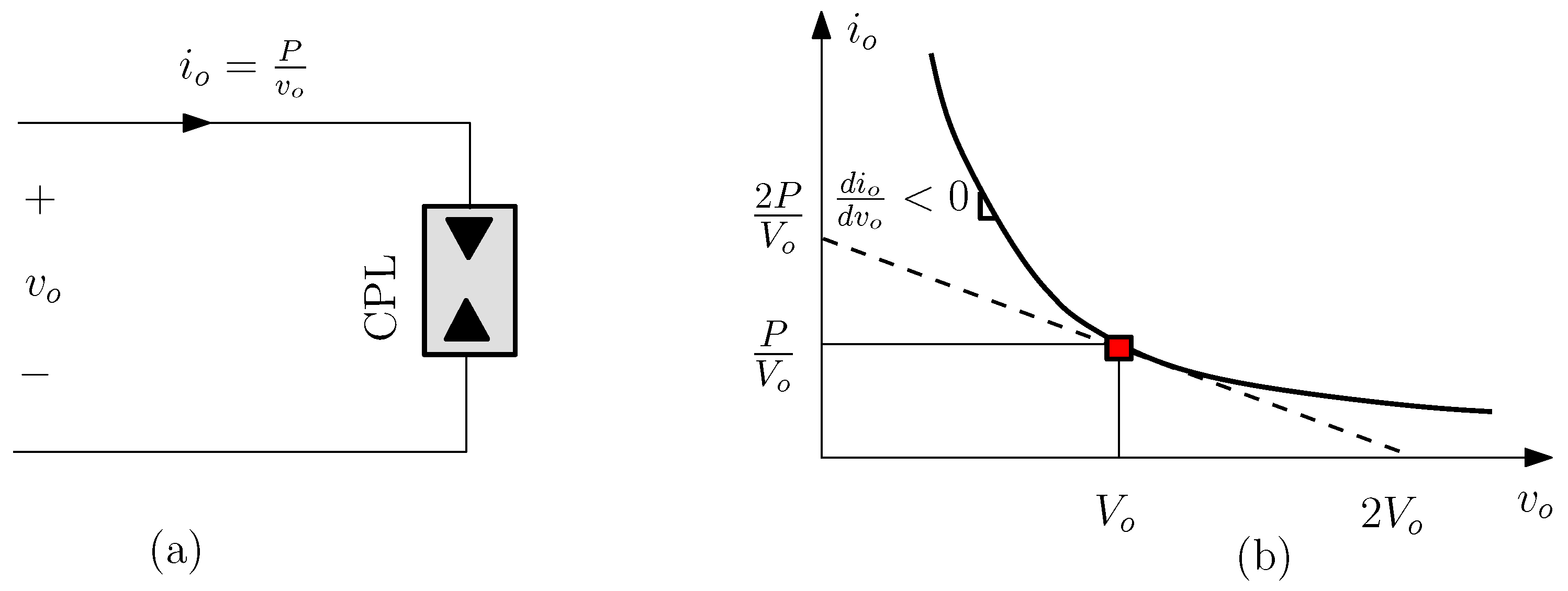
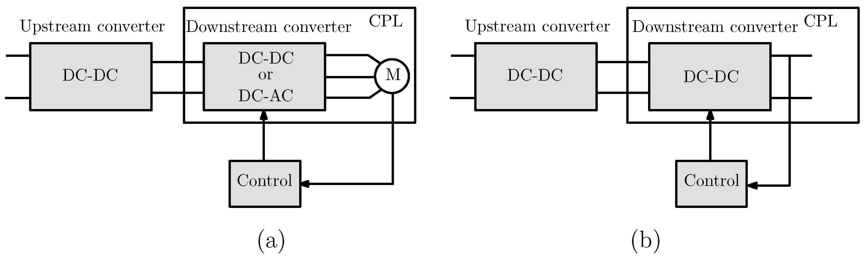
2. The Destabilizing Effect Associated with the Negative Impedance Due to the CPL Behavior

CPLs do not exist in nature but their behavior arises in switching converters feeding either other downstream converters or motor drives. A block diagram of a CPL is shown in Figure 2a and its voltage-current characteristic is shown in Figure 2b. Often, the CPL model considered is a static nonlinear current sink whose power is constant. This is because an increase in the CPL voltage results in a decrease in its current and the hence the product of both variables is kept constant [1,9,11,12]. The equation describing the current through a CPL in terms of the voltage across it is given by the following expression [14]:
i o = P v o .
In linear terms, the local resistance of the CPL can be obtained by linearizing the previous equation in the vicinity of an operating point ( V o , P / V o ) established by the load converter or the motor drive system. Close to this operating point, a CPL can be described by the following linearized model [14]
i o P V o + v o V o R o .
where R o = ( i o v o ) 1 . Therefore, the model of the CPL in the vicinity of the operating point can be represented by a straight line that is tangent to the nonlinear hyperbolic curve at the operating point with a negative slope equal to R o 1 in the voltage-current space. The equation for this line is given by (2). This model represents a current source I o in parallel with the negative resistance R o and these are given by the following equations:
R o = V o 2 P , I o = 2 P V o
As a result, although the local resistance at a certain point is positive, the corresponding incremental resistance R o is negative and this is known to produce instabilities to the system to which the CPL is connected [1,7,11]. As an example, consider the first-order nonlinear network depicted in Figure 3 which could represent an approximate circuit model for a boost converter under current-mode control and loaded by a CPL. The current at the input port is imposed to be the current limit I lim and this port can be considered as a constant power source (CPS) whose power is totally delivered to the nonlinear network. This power source models how this ideal power transfer takes place from the input port to the output port.
From KCL, the equation describing the dynamic behavior of the network of Figure 3 can be written in the following form:
C d v o d t = δ P v o ,
where δ P = P g P , P being the power of the CPL and P g = V g I r the power delivered from the input voltage generator.
For this particular system, the response can be derived mathematically without linearization. Indeed, by making the change of variable x ( t ) = v o 2 ( t ) , the previous equation can be expressed as follows:
d x d t = 2 δ P C ,
whose time-domain solution is given by the following expression:
x ( t ) = x ( 0 ) + 2 δ P C t ,
or equivalently in terms of the original state variable v o ,
v o ( t ) = v o 2 ( 0 ) + 2 δ P C t
Three different cases arise depending on δ P . These are:
  • δ P > 0 , the response is unbounded, and therefore the system is unstable.
  • δ P = 0 , the response is bounded but present an infinite number of equilibria depending on the initial condition v o ( 0 ) . Indeed, in this case, one has v o ( t ) = v o ( 0 ) t .
  • δ P < 0 , the response collapses at a certain time instant t c given by
    t c = C 2 δ P x ( 0 )
At this time instant, the voltage v o across the CPL becomes zero and its current becomes infinite. For t > t c , no real solution exists for the network equation. Figure 4 shows the responses corresponding to the previous three different cases.

3. Discrete-Time Modeling of a Boost Converter Loaded by a CPL

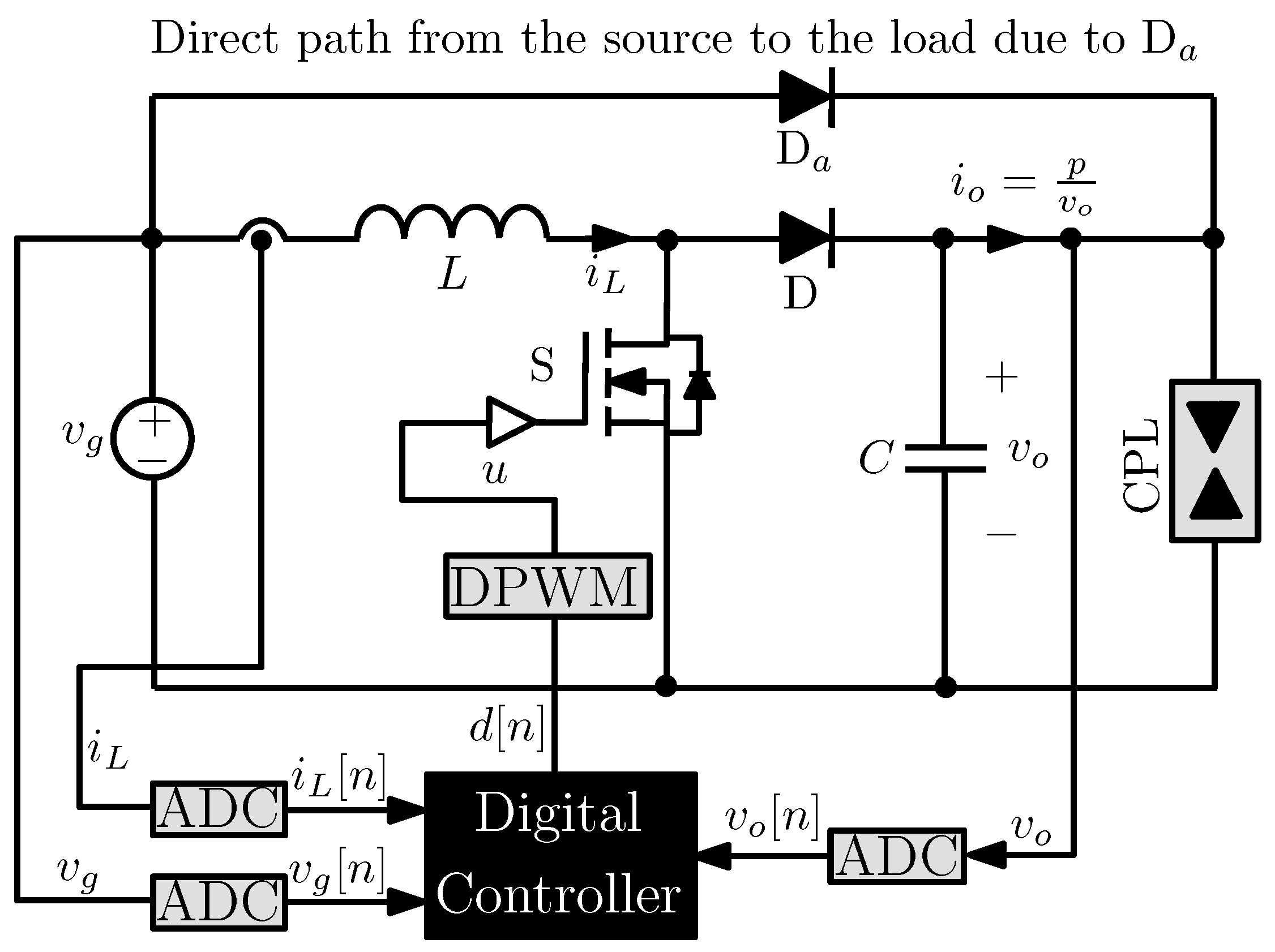
3.1. System Description

The results presented in this section and the sections coming later correspond to the boost converter depicted in Figure 5. However, the same approach can be applied to other converter topologies. The aim of the digital controller is to provide the suitable duty cycle for ensuring output voltage regulation and inducing sliding-mode regime in discrete-time. For that, the variables needed for the synthesis of the controller, are first converted into digital signals using analog-digital converters (ADC) at the rate of the sampling frequency and then processed by the controller. Selecting a proper sampling rate is important. Multi-sampling is a recently used approach in switching converters resulting in a sampling frequency larger than the switching frequency. This possibly will lead to unnecessarily overloading the digital processor. On the other hand, there are also some approaches using a sampling frequency shorter than the switching frequency. With this approach the controller will possibly miss dynamics of the power stage downgrading the performance of the closed-loop system. In switching converters applications, the duty cycle is updated once per switching period, for acceptable performance, it is quite appropriate to select the sampling frequency equal to the switching frequency which lead to a good compromise between accuracy and computing efficiency.
The regulation of the output voltage v o is required since disturbances in the output power p and the input voltage v g can take place. What is more, with CPL, closing the output voltage loop is also necessary for stabilizing the system since with voltage loop open it is unstable as will be shown later. The regulation can be accomplished by an outer voltage loop making the current reference i ref [ n ] to be the output of this loop. Figure 6 shows a double-loop control scheme, which is used for output voltage regulation while performing current limiting. The voltage controller consists of two stages. Namely, a digital PI block to process the error ε [ n ] : = V ref v o [ n ] and a limiter to avoid that the current reference overpasses an admissible level. The current controller is based on a DSMC strategy to be described below. This controller together with the digital PWM (DPWM) directly provides the duty cycle of the driving signal u of the converter MOSFET. The auxiliary diode D a in the power stage of Figure 5 is usually not present in the conventional DC-DC boost converter topology. It has been added to create a unidirectional path from the source to the load hence guaranteeing the condition v o = v g at the starting time and this helps to minimize the effect of the inrush current in the inductor as will be detailed later. It is worth noting that this condition is also required for the model of the load converter as a CPL to be valid. Indeed, the ideal static behavior of a CPL corresponds to the actual power absorbed by a converter acting as a load in a cascade connection with the source converter. However, while the tightly regulated load converter can be considered locally as a CPL for the source converter, this model is not valid for all the operating range of the interconnected system. In fact, the voltage drop across an ideal current sink (the CPL) is not defined unless there is some voltage applied to it. In [7], a small voltage limit is used as a threshold value for the load voltage to decide if an ideal static CPL behavior or an open circuit behavior must be used when performing numerical simulations. In cascaded converters, this voltage is the output of the source converter which cannot be tightly regulated in the case of a boost converter unless it is larger than the input voltage of the same converter. The requirement of output voltage at least equal to the input voltage in this converter can be easily met in the presence of the auxiliary diode D a in the boost converter power stage as shown in Figure 5. This diode guarantees that v o v g t in a normal operation of the boost converter.

3.2. Discrete-Time Mathematical Modeling

The development of a digital controller using DSMC concepts is performed in a discrete-time state-space formulation. Hence, for DSMC design, a discrete-time model of the power stage is first needed. Due to the presence of the nonlinear CPL, such a model cannot be exactly obtained in closed form. This is because, in contrast to switching converters with linear loads, the differential equations of the system for each switch position are nonlinear and cannot be solved in closed form. To overcome this handicap, we deal with the problem approximately by discretizing the averaged model which can be written as follows
d i L d t = v o L ( 1 d ) + v g L
d v o d t = p C v o + i L C ( 1 d )
where d is the duty cycle, all parameters and variables appearing in (9)–(10) can be identified in Figure 5. The key issue in the discrete model is the nonlinear differential Equation (10) associated with the dynamics of the capacitor in parallel with the CPL. The discrete-time model corresponding to this equation cannot be obtained in closed form. Different approaches can be used for obtaining an approximate discrete-time model. These are the Euler forward, Euler backward, and the Tustin (trapezoidal) methods [41]. For sufficiently small switching/sampling period, all these approximations yield similar results. For the sake of simplicity, let us choose the Euler forward approach for obtaining the discrete-time model. A discrete-time model can be obtained by approximating the continuous-time derivatives by their equivalent rate of change, hence assuming in the averaged model (9)–(10) that d i L / d t ( i L [ n + 1 ] i L [ n ] ) / T and that d v o / d t ( v o [ n + 1 ] v o [ n ] ) / T , where T is the switching/sampling period. The previous forward Euler approximation leads to the following discrete-time model of the system:
i L [ n + 1 ] = i L [ n ] + T L ( v g v o [ n ] ) + T L v o [ n ] d [ n ]
v o [ n + 1 ] = v o [ n ] T C i L [ n ] d [ n ] + T C ( i L [ n ] p v o [ n ] )
Notice that with a constant duty cycle value d [ n ] = D (open-loop operation), the coordinates of the equilibrium point are V o = V g / ( 1 D ) and I L = P / V g , where P and V g are the nominal values of the power p and the input voltage v g . It should be noticed that the steady-state inductor current, in contrast to the case of resistive load, inductor current coordinate of the equilibrium point does not depend on the operating duty cycle and is only imposed by the power P of the CPL and the input voltage V g . Moreover, the equilibrium point is unstable for all values of D ( 0 , 1 ) .
When sampling the state variables at the beginning of the switching cycle, depending on the modulation strategy, the samples in (11)–(12) can correspond to the peak values (leading-edge modulation), the valley values (trailing-edge modulation) or the average values (double-edge modulation). Here, a double-edge modulation will be used and the samples at the starting of each switching period will coincide with the averages.

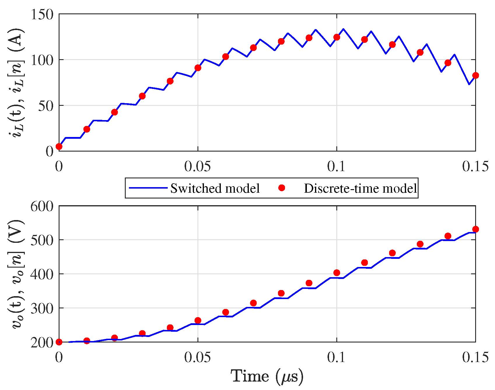
3.3. Open-Loop Model Validation

We will show below that the approximate discrete-time model (11)–(12) is enough accurate for control design. The results from this model are compared with those from the circuit-level switched model implemented in PSIM © software. Figure 7 shows the samples of the capacitor voltage and the inductor current obtained from (11)–(12) and the waveforms of the same variables obtained from the switched model. As can be observed, there is a good agreement between the results and therefore (11)–(12) can be faithfully used for digital control purposes. Please note that the dynamics of the inductor current is accurately predicted, and that the approximation only induces a relatively small loss of accuracy in predicting the samples of the output capacitor voltage. The small deviation can be perfectly compensated by the controller imposing the closed-loop poles at a desired position.

4. Digital Sliding-Mode Inner Loop Control Design

4.1. Large-Signal Model with Voltage Loop Open

Let x = ( i L , v o ) be the vector of the state variables of the power stage circuit. With the aim to control the samples of the inductor current i L [ n ] to their desired reference i ref [ n ] , the following discrete-time sliding surface is used
Σ = { x | σ [ n ] : = i ref [ n ] i L [ n ] = 0 }
When the voltage loop is open, the current reference i ref [ n ] is given in a fixed pattern i.e., without any feedback loop. Although this is a not a normal operation of the converter, the situation arises during startup while limiting the inrush current and the current reference remains constant at a certain constant limit I lim during this phase.

4.2. Equivalent Control

In a fixed-frequency DSMC of switching converters, the control variable d [ n ] during a certain switching period is selected in such a way that the controlled variable is imposed to catch its reference one period later. Therefore, the duty cycle d [ n ] is obtained by imposing the discrete-time sliding-mode condition σ [ n + 1 ] = 0 in (13) and solving for d [ n ] . In doing so, the following expression for the duty cycle (equivalent control) is obtained
d e [ n ] = L ( i ref [ n + 1 ] i L [ n ] ) T v o [ n ] + v o [ n ] v g [ n ] v o [ n ]
The value of the duty cycle is constrained within the interval (0,1) and the effective expression of the duty cycle becomes
d [ n ] = sat ( d e [ n ] )
where sat ( · ) stands for the saturation function defined by:
sat ( x ) = 1 2 1 + | x | | x 1 |
The saturation will not take place whenever 0 < d e [ n ] < 1 requiring the following condition to be satisfied:
i ref [ n + 1 ] T v g [ n ] L < i L [ n ] < i ref [ n + 1 ] + T ( v o [ n ] v g [ n ] ) L
At the initial time ( n = 0 ) without the presence of the diode D a , the previous constraints have no solutions and the system may have serious problems to startup. With initial conditions i L ( 0 ) = 0 and v o [ 0 ] = v g [ 0 ] (presence of diode D a ), the previous condition becomes
i ref [ 1 ] < T v g [ 0 ] L
If the previous constraint is not fulfilled, the system can startup easily, but the duty cycle will be saturated during a few switching cycles.

4.3. Comparison with State-of-Art Digital Predictive Control

Before continuing our study on the DSMC of the boost converter loaded by a CPL, we will present a short comparison with the Digital Predictive Control (DPC) published in [42]. To make the comparison clear and easy to follow, let us consider that the current reference i ref , the output voltage v o and the input voltage reference v g are constant ( v o [ n ] = V o and v g [ n ] = V g n N ). Please note that these are the same operating conditions used in [42] when deriving the control law. The fixed-frequency DSMC will be later applied separately using the full-order model of a boost converter loaded by a CPL. When applied to the DC-DC boost converter, the duty cycle in the case of DPC is given by the following expression:
d [ n ] = 2 D d [ n 1 ] + L ( i ref i L [ n 1 ] ) T V o
Under the same conditions, from (14), the expression for the duty cycle (equivalent control in (14)) for the case of the DSMC becomes
d [ n ] = D + L ( i ref i L [ n ] ) T V o
where in both cases D = ( V o V g ) / V o is the steady-state value of the duty cycle d [ n ] . There is a fundamental difference between the two control laws. While it can be observed that the duty cycle d [ n ] synthesized by the fixed-frequency DSMC approach is generated according to a static control law in which, at a certain switching cycle, its value is given directly in terms of the samples of the state variables and parameters at the same cycle, it is not the case of (19) which describes a dynamic control law for synthesizing the duty cycle d [ n ] , hence increasing the total order of the system by one. The equivalent control law based on the DSMC is static and does not change the order of the system. In the DSMC case, the current reference i ref will be caught in one cycle by the inductor current i L [ n ] assuming the output voltage constant while with the DPC two switching cycles are needed for the reference to be reached by the inductor current under the same operating conditions. Indeed, by linearizing the closed-loop system corresponding to DSMC and DPC, both approaches correspond to a dead-beat response. Notice that in linear digital control theory, the dead-beat control consists of finding the control law that when applied to a system, it brings the output to the steady state in several sampling cycles equal to the order of the system. To achieve this target, the control law places all the poles of the closed-loop transfer function at the origin of the z-plane.
Let I L and D be the nominal steady-state values of i L [ n ] and d [ n ] respectively. Let i ^ L [ n ] = i L [ n ] I L , d ^ [ n ] = d [ n ] D . The linearized model of the closed-loop boost converter under the DSMC is given by:
i ^ L [ n + 1 ] = 0
This is a 1-dimensional system with a pole at 0 and the current reference will be reached in one switching period. The linearized model of the closed-loop boost converter under the DPC is given by:
i ^ L [ n + 1 ] = i ^ L [ n ] + T L V o d ^ [ n ]
d ^ [ n + 1 ] = d ^ [ n ] L T V o i ^ L [ n ]
The Jacobian matrix corresponding to the previous model can be expressed as follows
J p = 1 T V o L L T V o 1
The eigenvalues of J p are the closed-loop poles of the boost converter under the DPC and are both located at 0. Therefore, with this control, the current reference will be reached in two switching periods. The numerical simulations depicted in Figure 8 shows the inductor current responses of the system under the DPC and the DSMC in front of positive and negative step changes in the current reference i ref between 5 A to 10 A. For ease of comparison, only the dynamics of the inductor current is conserved while the output voltage was fixed to V o = 380 V with L = 326 μ H and f s = 100 kHz and V g = 200 V. These responses confirm the previous theoretical remarks about the dead-beat nature of the responses of the two control strategies.

4.4. DSMC Design

To guarantee convergence of the trajectories of the system to the sliding surface Σ , the following reaching conditions must hold
σ [ n + 1 ] 0 if Δ σ [ n ] 0
where Δ σ [ n ] : = σ [ n + 1 ] σ [ n ] is the increment in function variable σ [ n ] during one switching cycle which can be obtained as follows
Δ σ [ n ] = i ref [ n + 1 ] i ref [ n ] + T L ( ( 1 d [ n ] ) v o [ n ] v g [ n ] )
Accordingly, (25)–(26) become as follows
v g [ n ] ( 1 d [ n ] ) v o [ n ] L i ref [ n + 1 ] i ref [ n ] T v g [ n ] L
The above inequalities mean that the reference current rate change must be bounded between the negative and the positive slopes of the inductor current during the charging and the discharging time intervals, respectively. In steady-state operation, these conditions are easily met. However, they can be violated during startup or during transient due to abrupt changes. The loss of sliding-mode operation could lead performance degradation manifested by either large overshoots or slow response.
When i ref [ n + 1 ] = i ref [ n ] (either constant or T-periodic), (28) becomes 0 v g v o . In this case, starting from zero initial conditions and without the presence of the auxiliary diode D a (See Figure 5), sliding condition will not be fulfilled at startup. With the presence of the auxiliary diode D a , the condition v o = v g is guaranteed from the beginning, the system starts in sliding-mode and immediately the system trajectory is constrained in the discrete sliding-mode domain defined by the constraint i ref [ n ] i L [ n ] = 0 . The worse cases take place when the duty cycle is saturated. For d [ n ] = 0 , Δ σ [ n ] = T L ( v o [ n ] v g [ n ] ) 0 (if v o [ n ] v g [ n ] ) and σ [ n + 1 ] 0 . For d [ n ] = 1 , Δ σ [ n ] = T L v g [ n ] 0 and σ [ n + 1 ] 0 , which ensures the convergence to the switching surface. It will be shown later that at startup, the current reference could be saturated, the voltage loop becomes open and the resulting system is unstable making the voltage v o to increase above v g hence guaranteeing the sliding-mode condition. When the output voltage reaches the vicinity of its desired value, saturation disappears and the PI regulator starts regulating the output voltage to its desired value according to the imposed performance by the outer loop controller design.

4.5. Control-Oriented Full-Order Discrete-Time Small-Signal Model

As stated before, in linear terms, the current loop presents a dead-beat response under the fixed-frequency DSMC and the DPC. However, the interaction with other state variables can only be revealed by considering the full-order model of the system. The focus on this paper is on the DSMC. Similar procedures can be followed for studying the DPC.
By substituting the expression of the equivalent control (14) in (12) and imposing the discrete-time sliding-mode constraint i L [ n ] = i ref [ n ] imposed by (13), one obtains the following equation describing the output capacitor voltage v o in the discrete-time domain
v o [ n + 1 ] = f v ( v o [ n ] , i ref [ n ] , i ref [ n + 1 ] , v g [ n ] , p [ n ] )
where the function f v is given by the following expression
f v ( v o [ n ] , i ref [ n ] , i ref [ n + 1 ] , v g [ n ] , p [ n ] ) = v o [ n ] + i ref [ n ] L ( i ref [ n ] i ref [ n + 1 ] ) + T v g [ n ] C v o [ n ] T p [ n ] C v o [ n ]
The equilibrium point of the discrete-time dynamical system described by (29)–(30) can be obtained by imposing v o [ n + 1 ] = v o [ n ] and i ref [ n + 1 ] = i ref [ n ] in the same equations. Imposing these constraints implies that v o [ n ] takes an infinite value unless the current reference i ref [ n ] is chosen to be exactly equal to p [ n ] / v g [ n ] . Indeed, this is the only inductor current value that correspond to a balance between the input power delivered by the voltage source and the output power imposed by the CPL. Therefore, during startup and while the system is under inrush current limiting phase, it is feeding a CPL with a constant current different from the one that balances input and output powers in the system and this explains the output voltage divergence in a similar way to the first case of the nonlinear network of Section 2. It is worth noting that for inrush current limitation during startup, the converter will unavoidably work under this condition. The output voltage will collapse if the current reference is smaller than P / V g . This fact appears in a clear contrast with the case of resistive load for which the voltage reaches a finite value in steady state when the system is under pure current-mode control [38]. The case studied here is similar to the analog control based on the average inductor current regulation in a buck converter loaded by a CPL, which is still unstable after the introduction of the current control loop [3]. In both cases, the introduction of an outer voltage loop will contribute to the global stabilization of the system apart from ensuring output voltage regulation. It should also be noted that when an outer loop is added to stabilize the output voltage while establishing the current reference, this current will be imposed to be I ref = P / V g in steady state regardless the desired reference value V ref of the output voltage v o .
Let V o and I ref be the nominal steady-state values of v o [ n ] and i ref [ n ] respectively. Let v ^ [ n ] = v o [ n ] V o , p ^ [ n ] = p [ n ] P , v ^ g [ n ] = v g [ n ] V g , i ^ ref [ n ] = i ref [ n ] I ref the small deviations of the output voltage v o [ n ] , the input voltage v g [ n ] , the current reference i ref [ n ] and the power p [ n ] with respect to their steady-state values V ref , V g , I ref and P respectively. Therefore, the small-signal model of the system under current-mode control can be written as follows:
v ^ o [ n + 1 ] = f v v o [ n ] v ^ o [ n ] + f v i ref [ n ] i ^ ref [ n ] + f v i ref [ n + 1 ] i ^ ref [ n + 1 ] + f v v g [ n ] v ^ g [ n ] + f v p [ n ] p ^ [ n ]
The different partial derivatives appearing in (31) are
f v v o [ n ] = 1 + T C v o 2 [ n ] ( P I ref V g ) , f v i ref [ n ] = T V g L I ref C v o [ n ] f v i ref [ n + 1 ] = L I ref C v o [ n ] , f v v g [ n ] = T I ref C v o [ n ] , f v p [ n ] = T C v o
With abuse of notation, let v ^ o ( z ) , v ^ g ( z ) , p ^ ( z ) and i ^ ref be the z-transforms of v o [ n ] , v g [ n ] , p [ n ] and i ref respectively.
Taking the z transform of (31), the i ref -to- v o , the v g -to- v o and the p-to- v o small-signal transfer functions of the digital sliding current-mode-controlled boost converter with voltage loop open and supplying a constant power can be expressed as follows
H i ( z ) = v ^ o ( z ) I ^ ref ( z ) = R i z z c z z p ,
H g ( z ) = v ^ o ( z ) V ^ g ( z ) = I ref T C V o 1 z z p ,
H p ( z ) = v ^ o ( z ) P ^ ( z ) = T C V o 1 z z p
where R i , z c and z p are given by
R i = L I ref C V o , z c = 1 + T V g I ref L , z p = 1 + T C V o 2 ( I ref V g P )
The previous transfer functions represent the discrete-time small-signal model of the boost converter under an inner current control loop based on a DSMC strategy and can be used to design an outer digital voltage control loop in the z domain. Please note that the zero z c of the i ref -to- v o transfer function H i ( z ) in (32) is outside the unit circle, which explains the well-known non-minimum phase characteristics of the control-to-output voltage transfer function in a boost converter. Also note that during the startup, the current reference i ref will be limited by an upper bound I lim which must be selected larger than the desired steady-state P / V g , hence, the pole z p of the previous transfer functions is outside the unit circle, which corresponds to an unstable system. Therefore, any designed controller must stabilize the system while regulating the output voltage and exhibiting desired performance in terms of disturbance rejection and transient response.

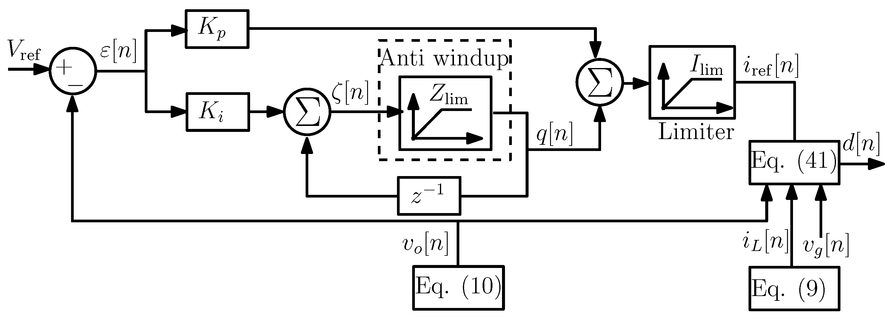
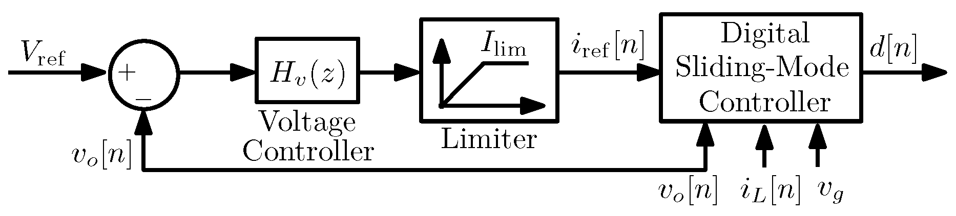
5. Digital Control for Output Voltage Regulation

To ensure an output voltage regulation, an outer and slower control loop in cascade with the inner DSMC current loop must be added. This loop is designed in the z domain based on the i ref -to- v o transfer function H i ( z ) in (32) representing the small-signal model around a desired operating point. This second control loop will regulate the output voltage to a desired value V ref . The steady-state current reference I ref will be equal to P / V g regardless the value of V ref as mentioned before. To stabilize the system, a two-loop control strategy will be used, hence the outer voltage loop provides the reference for the inner current loop. Let ε [ n ] = V ref v o [ n ] be the output voltage error. The current reference is updated from the output of a digital PI compensator as follows
i r [ n ] = K p ε [ n ] + q [ n ]
where q [ n ] = K i k = 0 n ε [ k ] is the discrete-time accumulative sum of the error voltage weighted by the integral gain K i being K p the proportional gain. In order to avoid high inrush current in startup, the current reference must be limited and the final expression for the current reference becomes
i ref [ n ] = i r [ n ] if i r [ n ] < I lim I lim if i r [ n ] I lim
Different approaches can be often used for integral control emulation. For sufficiently small switching/sampling period and all the approaches yield a controller which produces a closed-loop behavior similar to the one provided by a continuous-time controller. For the sake of simplicity, let us choose the Euler forward approach for emulating the integrator. This approximation yields the following recurrence equation for the discrete-time integral variable:
ζ [ n + 1 ] = ζ [ n ] + K i ε [ n ]
where K i is the integral gain. To avoid windup phenomenon, the integral variable ζ [ n ] is also limited to an upper bound Z lim and the expression of the variable q [ n ] becomes as follows
q [ n ] = ζ [ n ] if ζ [ n ] < Z lim Z lim if ζ [ n ] Z lim
The presence of an advanced sample of the current reference i ref [ n + 1 ] in the expression of the control law (14) makes it challenging to obtain this law when the reference is to be provided by a feedback loop. A possible solution is to use a predictive approach to get the value of the reference current from (36) one switching period ahead of time using (12). While this would work theoretically and in simulation, it would require increased computational resources in an experimental digital platform such as a DSP. A much simpler solution is to redefine the discrete-time sliding-mode surface as follows:
σ [ n ] = i ref [ n 1 ] i L [ n ]
and the resulting expression of the duty cycle becomes
d [ n ] = sat L ( i ref [ n ] i L [ n ] ) T v o [ n ] + v o [ n ] v g [ n ] v o [ n ]
The first term in the expression of d [ n ] in (41) is non null only in the reaching phase. Once the sliding-mode regime is reached, this term becomes zero and only the second term forces the system to evolve toward the equilibrium point if the stability of the closed-loop system is ensured.
Figure 9 shows a block diagram of the large-signal model of the system with a two-loop control based on DSMC. The presence of a discrete-time integrator in the external voltage loop will impose that in steady state V o : = v o [ ] = V ref . Furthermore, in steady-state one will have Q : = q [ ] = i L [ ] and I L : = i L [ ] = P V g . Therefore, the coordinates of the equilibrium point are
I L = P V g , V o = V ref , Q = I L = P V g
where I L , V o and Q stand for the steady-state values of the state variables i L , v o and q respectively.

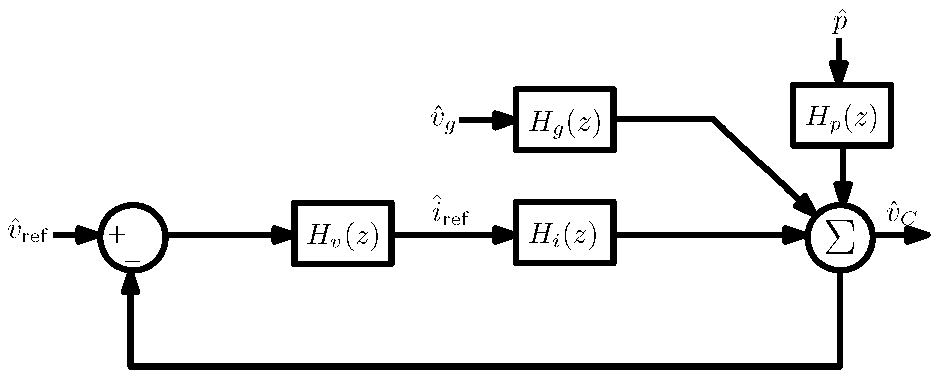
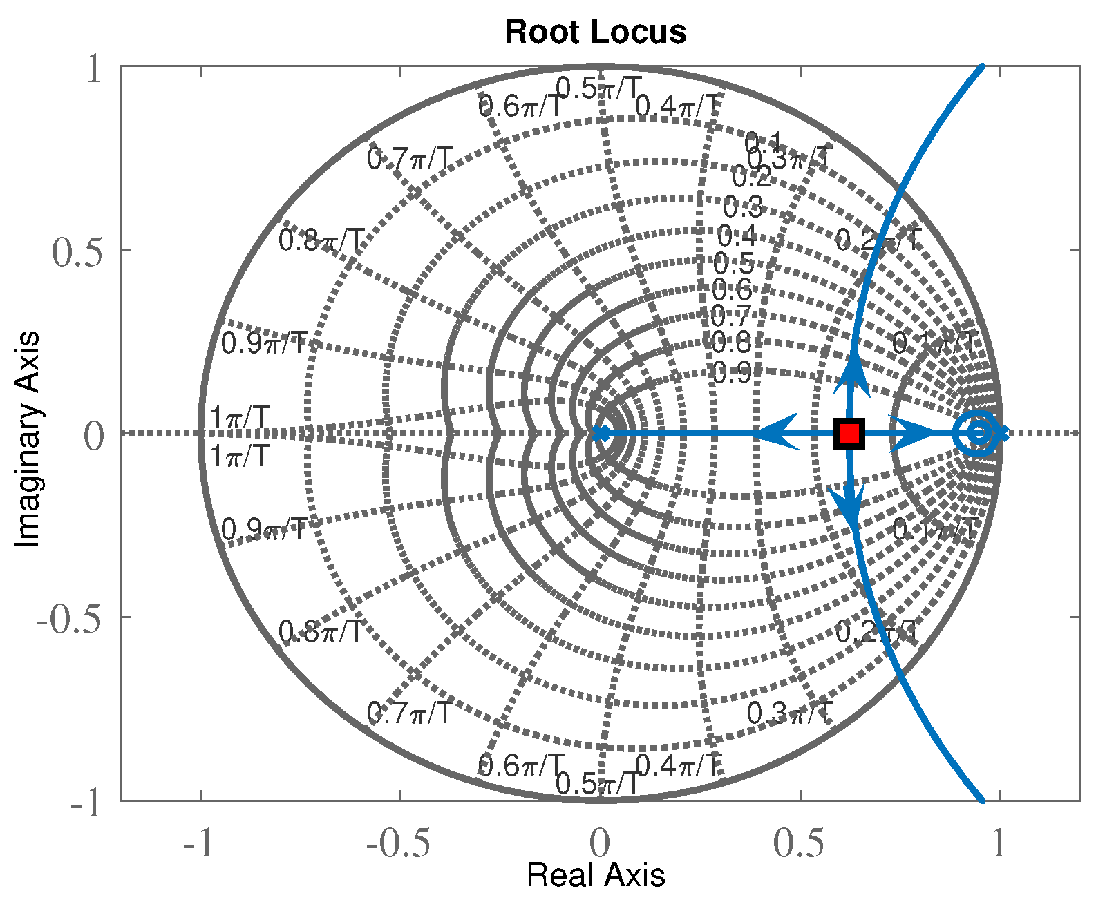
6. Design of the Output Voltage Feedback Loop Using the Root-Locus Technique

The block diagram corresponding to (31) is depicted in Figure 10. The small-signal model can be used to design the feedback compensator to obtain a stable closed-loop system with a regulated output voltage.
The focus in this section is on the design of the output voltage regulator. The time response characteristics are related to closed-loop pole locations. Hence, a design based on root-locus approach will be used. The aim is to design a controller such that the dominant closed-loop poles have a desired damping ratio ζ and a settling time t s . According to (36) and (38), the transfer function for the outer digital PI voltage controller can be expressed as follows
H v ( z ) = K p + K i z 1 K p z z pi z 1
where z pi = 1 K i / K p is the zero introduced by the digital PI compensator. The loop gain of the system is
L ( z ) = H i ( z ) H v ( z ) = K p R i ( z z pi ) ( z z c ) z ( z 1 ) ( z z p )
Please note that because of the one cycle delay present in the current reference in (40), a pole at the origin is added to the loop gain.
Although (44) can be used to obtain numerically the suitable parameter values for the desired pole position, it is always more useful to have an explicit mathematical expression. For many applications, the feedback gain K p is a design parameter that should be adjusted accordingly to the values of other parameters to get a system response with the desired performance. The purpose in this section is to perform an analytical study by carrying out a realistic approximation. Unfortunately, there is no universal procedure to approximate the loop gain. To simplify the design, the integral gain K i = K p ( 1 z pi ) can be appropriately selected so that the zero of the PI controller is placed slightly smaller than 1. This means that the term K i / K p must be selected much smaller than 1 and the loop gain can be approximated by
L ( z ) K p R i z z c z ( z z p ) ,
The approximate closed-loop characteristic polynomial equation can be expressed as follows
1 + L ( z ) = 0 z 2 ( K p R i + z p ) z + K p R i z c = 0
The closed-loop poles can be selected at the break-away point z ba on the real axis to correspond to a damping factor ζ = 1 and a settling time t s = 4 T / ln | z ba | . For finding the break-away points, one must find the value of z = z ba that maximizes or minimizes the gain K p [41] hence obtaining the following approximate expression for the values of the break-away points and the corresponding proportional gain of the PI controller
z ba z c ± z c 2 z p z c , K p , ba ( z ba z p ) z ba R i ( z ba z c )
The value of z ba with positive sign is omitted because it corresponds to a break-in point outside the unit circle leading to an unstable system.

7. Numerical Simulations and Model Validation

7.1. System Startup and Steady-State Operation

The initial value of the duty cycle can be obtained from the initial values of the state variables. Usually, the obtained value at startup is saturated. With delay, the number of initial saturated cycles increases since the inductor is continuously charged during a few cycles leading to an increase of the inrush current.

7.1.1. Validation of the Closed-Loop Large-Signal Model and Guaranteeing the Sliding-Mode Operation

Let us consider the nominal values of the power stage parameters, the desired output voltage and the switching frequency depicted in Table 1. The steady state of the current reference is I ref = P / V g = 5 A. During the startup, the current reference i ref and the integral variable q were limited to I lim = 10 A and Q = 10 A, respectively. The PI zero is selected at z c = 0.95 . First, the root locus of the closed-loop system is obtained and the result is depicted in Figure 11. Let us select the closed-loop poles at the break-away point z ba 0.62 + 0 j which corresponds to a proportional gain K p 0.82 , damping coefficient ζ = 1 .
The performance of the DSMC will be validated by means of numerical simulations from both the derived large-signal discrete-time model and from a detailed switched model implemented in PSIM © software.
Figure 12a shows the startup and the steady-state responses of the system from both models. It can be observed that during startup the inductor current reference i ref = I lim remains constant due to the saturation hence limiting the inrush current. As soon as the capacitor voltage reaches the vicinity of the voltage reference V ref , the PI controller comes to play and the current reference is no longer constant but time varying, state-dependent and provided by the PI compensator according to (36). The data from the discrete-time model are plotted together with the simulated data from the detailed switched model implemented in PSIM © software. It can be observed that the responses from the two models are very close. The voltage waveforms from the switched model and the discrete-time model cannot be distinguished from each other. Hence, the above simulations show that the large-signal model derived in this work can predict accurately the large-signal behavior of the system.
Remark 1.
Since during startup the average inductor current value is the regulated variable and it is supposed to reach the reference current in one cycle, the ripple of this variable can only exceed the limit I lim by the switching ripple Δ i L given by
Δ i L = T v g ( v o V g ) 2 v o L
At the initial time, v o = V g due to the presence of the auxiliary diode D a and Δ i L should be zero as can be confirmed in Figure 12a. However, in a practical implementation of a digital controller, saturation of the duty cycle during the initial cycles and propagation delays always exist and it is expected that the average inductor current will still overpass the imposed current limit. The current ripple amplitude Δ i L from (48), superposed to the averaged current I L is plotted in the bottom panel of Figure 12a together with the current waveforms obtained from the switched model. The agreement is remarkable both in the startup, in steady state and in the transient phase.
It is worth noting that one cycle delay inherently existing in the used commercial device has been eliminated by appropriately modifying the C code programming of the device. However, computation delay is unavoidable. By adding a computation delay τ d = 5.5 μ s, the results depicted in Figure 12b are obtained where it can be observed that a small inrush current still exists in the current startup response. The value of the computation delay used is the one corresponding to the experimental prototype to be described later. The propagation delay makes higher the number of cycles during which the duty cycle is saturated making the sliding-mode condition not satisfied during these cycles which in turns lead to higher inrush current at startup. As a remedy of this problem, one can force the initial values of the duty cycle to lie within the interval (0,1) in a few cycles either by scaling down the value of the duty cycle obtained from the control law (41) or by limiting the rate of change of the reference current from zero to I lim in startup. The last solution will be adopted later in the section related to the experimental validation of the results.
By filtering out the high frequency component of the current reference at the abrupt change in startup, the inrush current can be suppressed. However, the presence of a filter also slows down the system response. Another way to limit the inrush current in the presence of computation delays without degrading the system response is by limiting the rate of change of the current reference during startup.
Remark 2.
The system is unstable when the saturation is taking place and the system is current-mode control with open voltage loop. During this phase, the output voltage tends to infinity although the average of the inductor current is theoretically well regulated to the maximum allowed current I lim . During this phase, the system operates like the nonlinear first-order network shown in Figure 3. In the case of the boost converter, this type of instability only makes the output voltage to increase from the initial voltage V g . This increase in the output voltage is desired since under this operation the system is approaching its desired operating point.

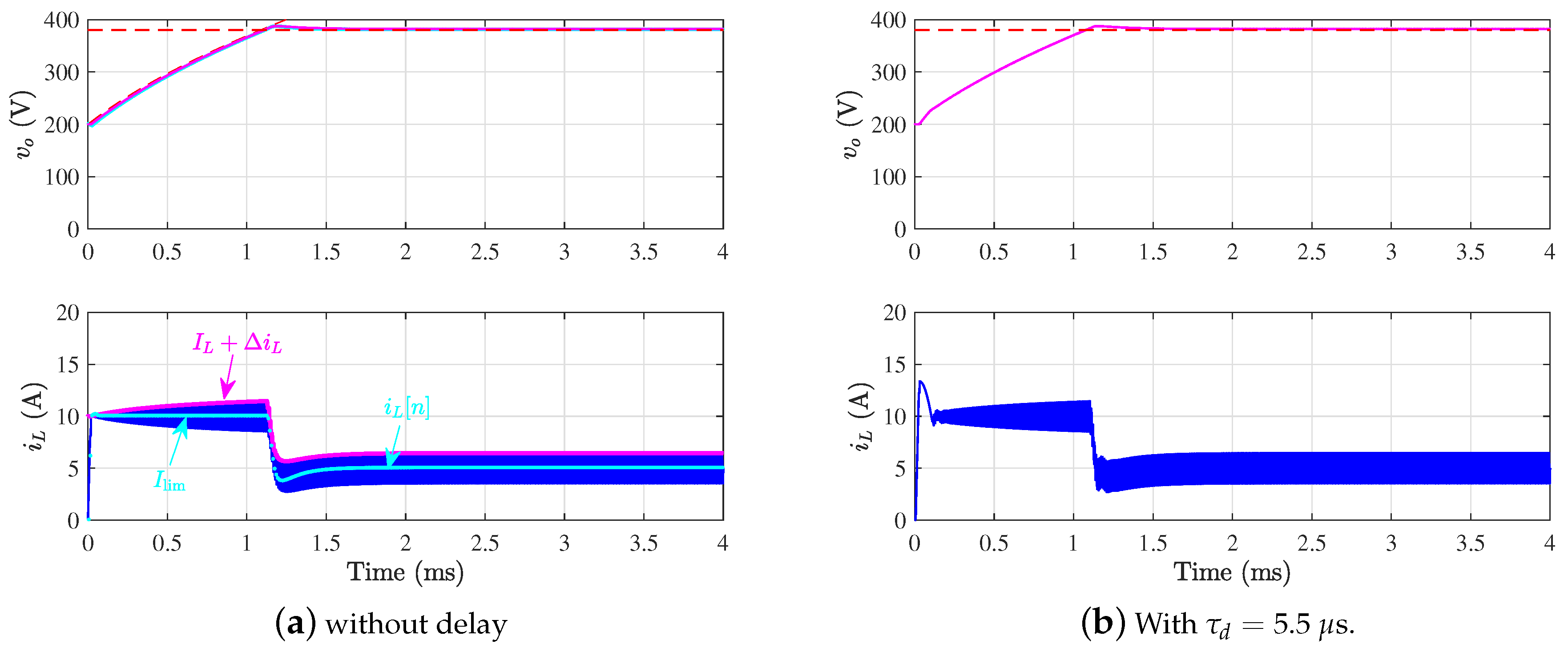
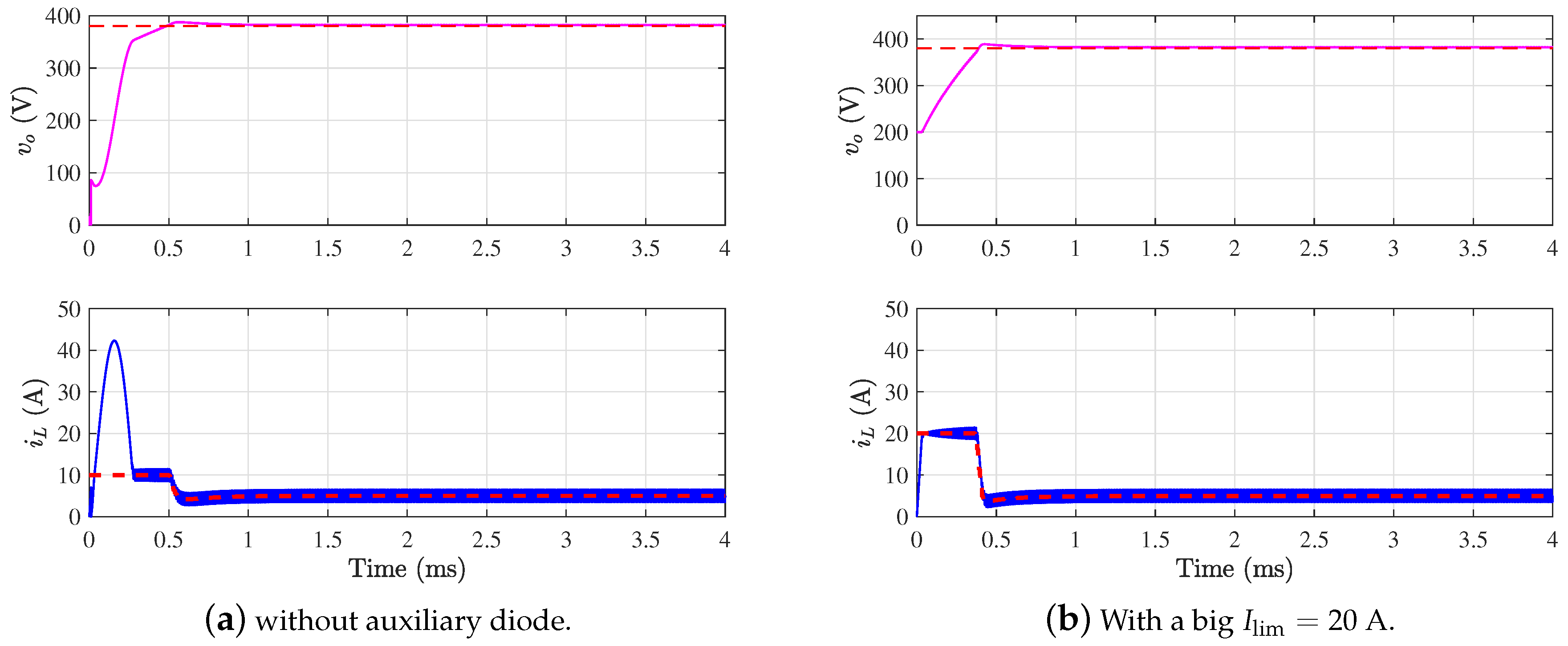
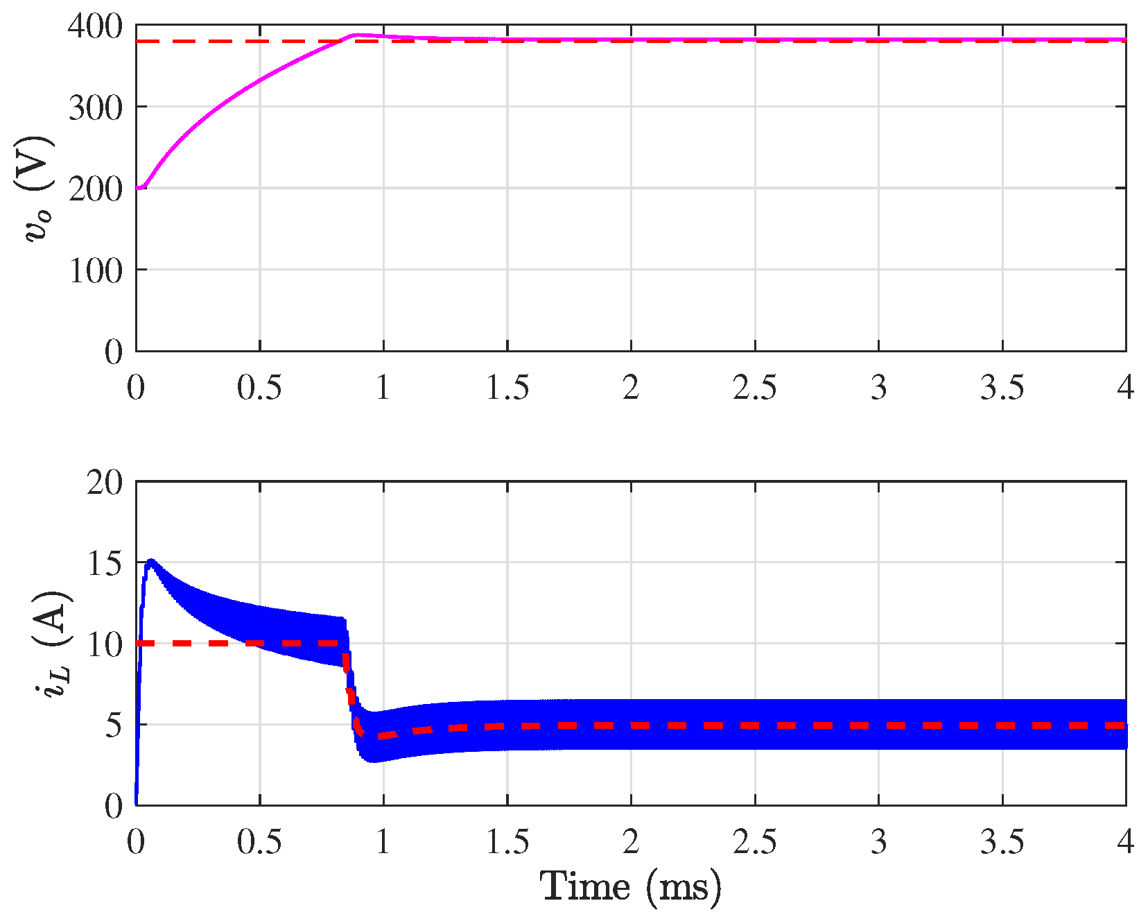
7.1.2. The Importance of Operating in Sliding-Mode Regime for Inrush Current Limitation

To reveal the importance of different aspects in the controller, some cases are simulated below.
Figure 13 shows the startup of the system with the sliding-mode non-guaranteed at startup with two different cases. In the first case (Figure 13a), the auxiliary diode D a is omitted and the system starts with zero initial condition. Without time delay, the system exhibits severe problems for starting-up. The inrush current in this case is very large even under current limitation. This is because since the sliding-mode operation is not guaranteed, the inductor current does not tightly track the limited current reference I lim . The mean reason is that since the output voltage is less than the input voltage, the driving signal is switched on and it remains on as long as i L [ n ] < I lim hence charging the inductor current. When i L [ n ] = I lim for the first time, the output voltage v o [ n ] is still smaller than the input voltage and sliding-mode condition is not yet satisfied. The output voltage increases, and the sliding-mode condition is satisfied as soon as the output voltage is equal to the input voltage. However, when this occurs, the inductor current has already reached a high value leading to an unacceptable inrush current. In the second case (Figure 13b), with the presence of the auxiliary diode D a , the sliding-mode condition (28) is guaranteed at startup but the non-saturated reference generated by the outer voltage loop is very high and the inductor current well tracks it which is undesirable. In the simulation instead of not using a limit for the current reference, a high value ( I lim = 20 A) is used.
It is worth noting that the DSMC derived in this study is based on a full-order representation of the system in the state space. In both DSMC and DPC, the control law is nonlinear since the output voltage appears in the denominator of the expression of the duty cycle. A discussion on approximating the samples of the output voltage by their constant steady-state values was presented in [42] concluding that it is reasonable to use the constant output voltage instead of its instantaneous samples. However, the startup and the transient response performance under this condition were not discussed and only steady-state behavior was evaluated. It should be noted that when the samples of the output voltage are substituted by their constant steady-state value, the controller becomes linear, and the computation effort is reduced. However, this occurs at the expense of losing the sliding-mode operation which in turns results on a high inrush current and unsatisfactory system performance during both startup and under transient response. In an experimental circuit, the high inrush current would even destroy the switching semi-conductor devices.
The expression of the duty cycle (equivalent control) contains the instantaneous values of the state variables and none of them is substituted by its constant steady-state value. This is indispensable for the system to work in sliding mode, which is crucial for inrush current limiting. This will change the system behavior during startup since the sliding-mode operation will be lost.
Figure 14 shows the startup response of the system when the samples of the output voltage are replaced by their steady-state value in (41) but using the instantaneous values of the output voltage in the expression of i ref given by (37). As can be observed, the current reference is not well tracked during the startup phase and the system exhibits an unacceptable inrush current hence demonstrating the importance of operating under sliding-mode regime which is guaranteed by using the instantaneous values of the state variables not their steady-state values.

7.2. Small-Signal Response to Output Voltage Variation. Non-Minimum Phase Behavior

Figure 15 shows the response of the system to a ± 4 V step change in the reference voltage using a switched model. It can be observed that the system exhibits a small undershoot in the output voltage response immediately after the positive step change of voltage reference. The inductor current follows the reference current tightly as dictated by the DSMC.

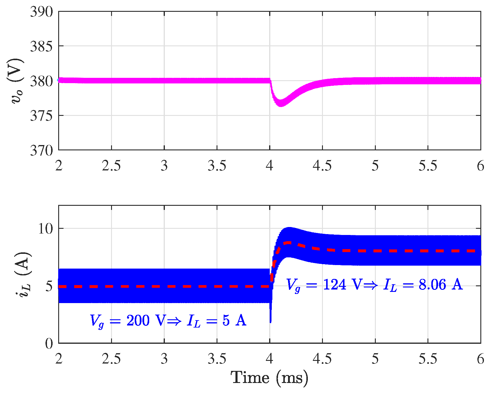
7.3. Small-Signal Response to Input Voltage Disturbance

Figure 16 shows the transient response in the presence of 38% step change in the input voltage from the detailed switched model implemented in PSIM © software. It can be observed that the output voltage is tightly regulated to its desired value. The steady-state average inductor current is I ref = P / V g as predicted by the theoretical analysis. The inductor current and capacitor voltage show a fast recovery of the steady state after a disturbance takes place.

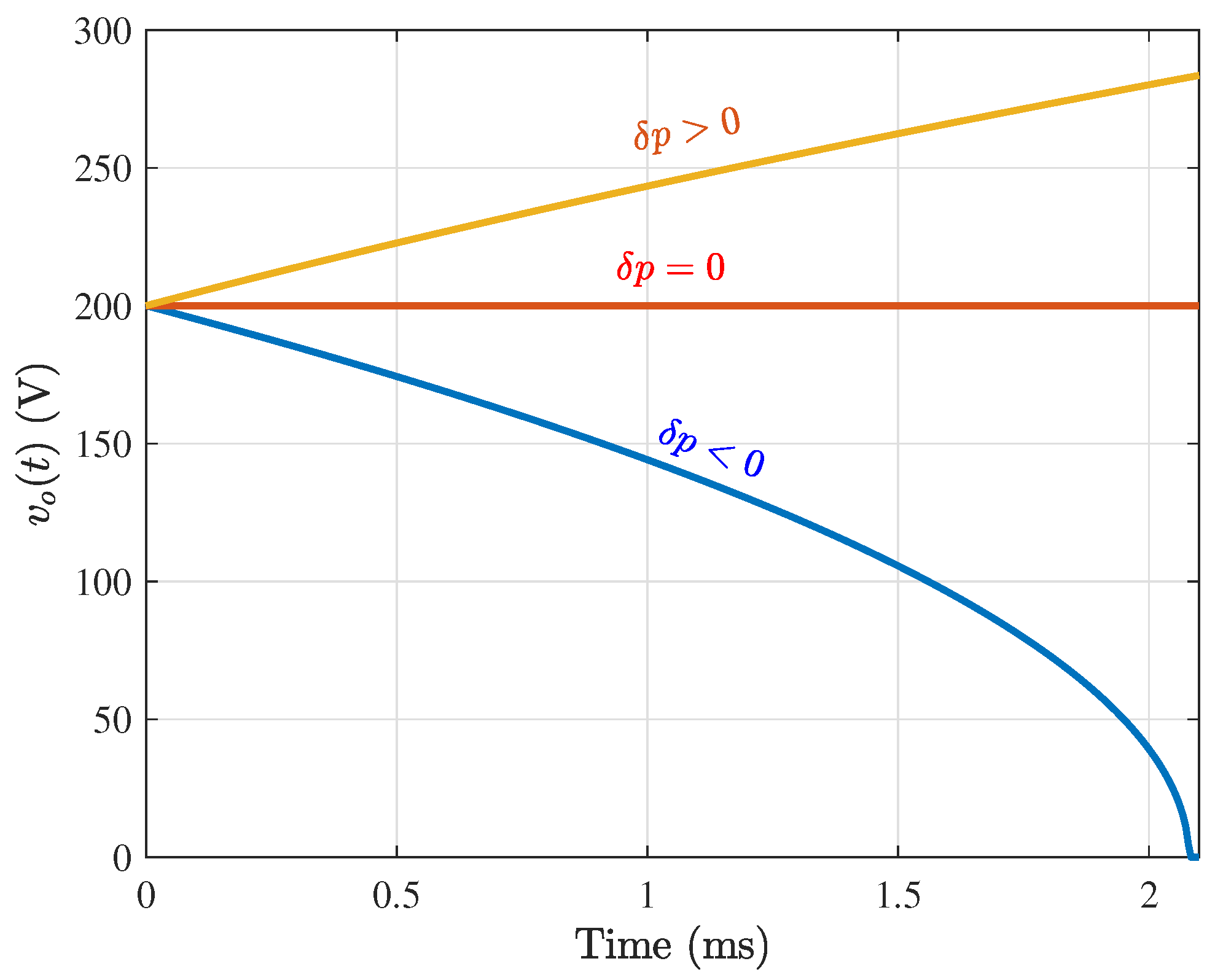
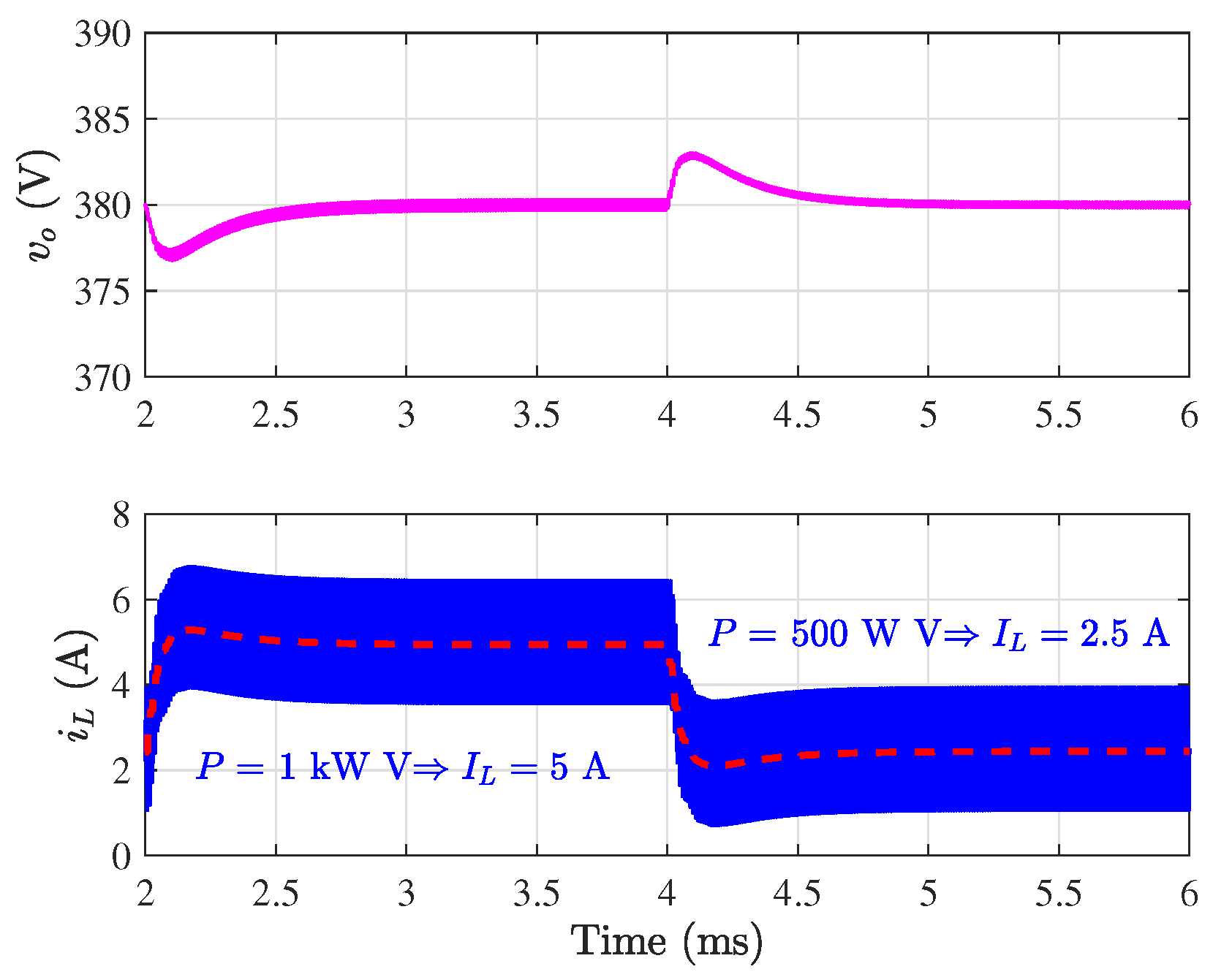
7.4. Small-Signal Response to Power Disturbance

Figure 17 shows the transient response in the presence of 50% step change in the load power from the detailed switched model. A zero steady-state error in the output voltage can also be observed while the dynamic current reference i ref is tracked by the inductor current i L as imposed by the inner DSMC loop. The steady-state value of i ref is I ref = P / V g as predicted by the theoretical analysis. As before, both inductor current and capacitor voltage show a fast recovery of the steady state. As can be observed, in all the cases, both small-signal and large-signal behaviors show a similar behavior, confirming the validity of the model developed in the previous sections. Hence the large-signal model can be used for repeated simulations while the small-signal model can be used for control design and performance specifications.
Remark 3.
Theoretically, according to the small-signal design procedure followed, the system should present no overshoot for a positive step change with the chosen values of parameters. However, a small overshoot can be still appreciated in the system response of Figure 15. The discrepancy is mainly due to the computation delay ( τ d 5.5 μs) not taken into account in the analysis.

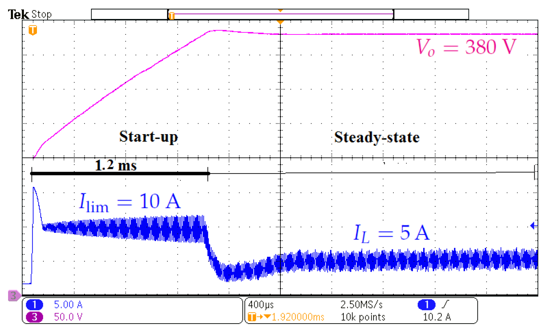
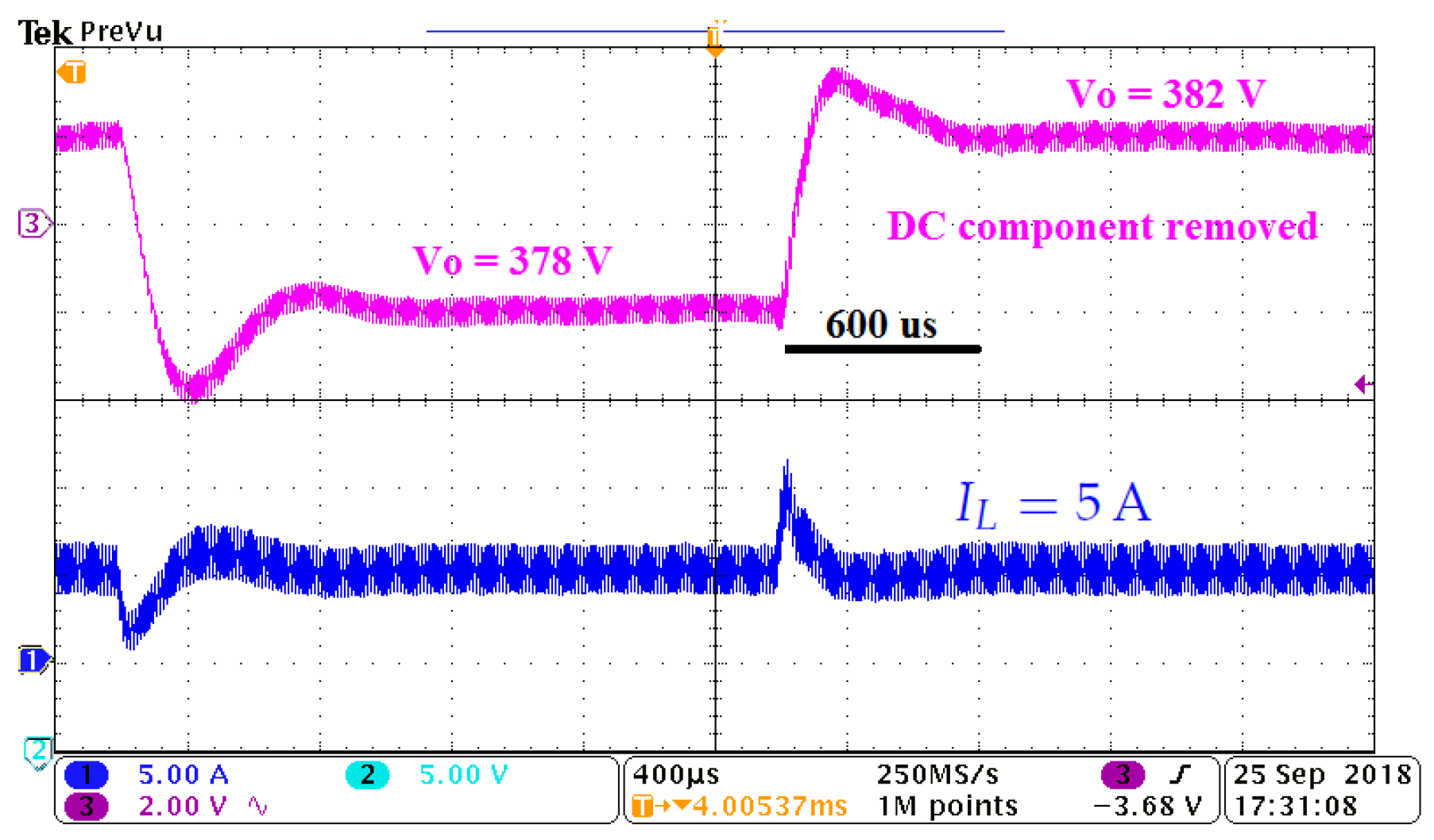
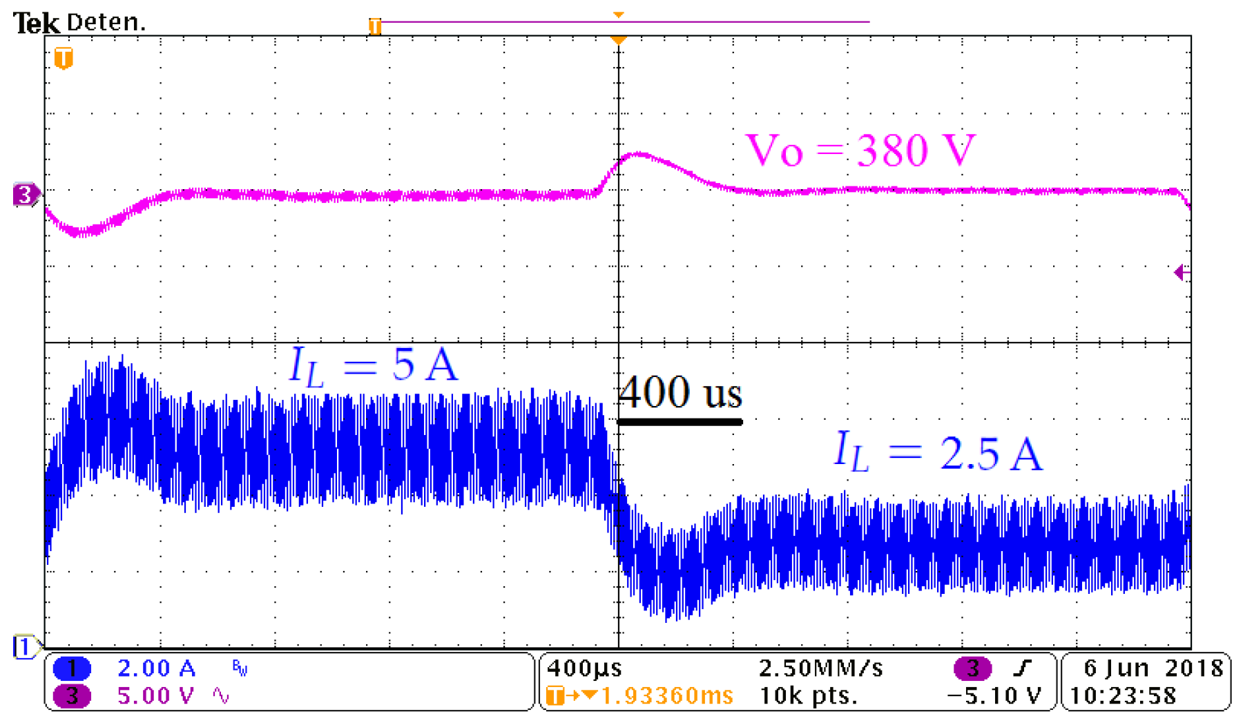
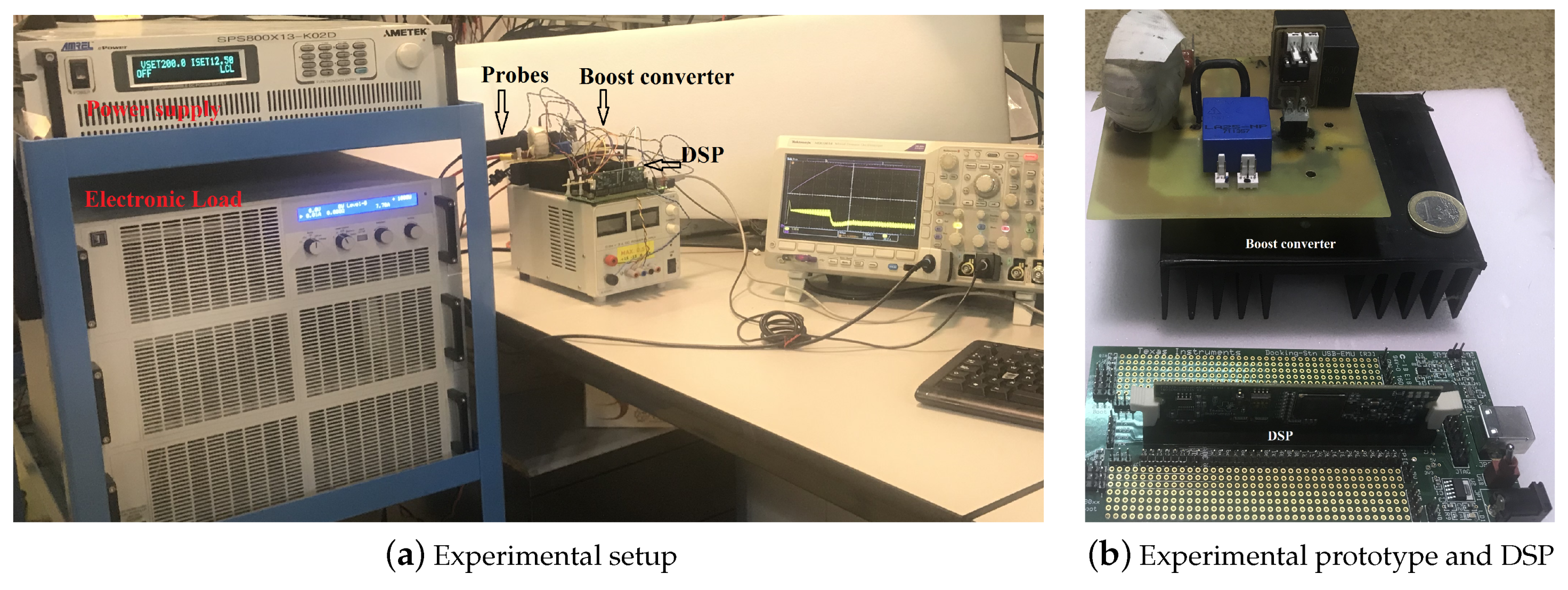
8. Experimental Results

8.1. Experimental Setup

A boost converter under DSMC was implemented to verify the validity of the control design approach proposed in the previous sections. A picture of the experimental benchmark and the implemented experimental prototype is depicted in Figure 18. The measured large-signal and small-signal response are compared with the theoretical predictions for the same set of parameter values and under the same conditions. The developed DSMC algorithm was programmed in the Digital Signal Processor (DSP) TMS320F28335 of Texas instruments. The samples of the state variables are captured and adapted to the voltage values supported by the DSP, connecting to a pin of the ADC module through an operational amplifier operating as a buffer to isolate the DSP. The signals are sampled at the switching frequency rate. The duty cycle was calculated according to (41) and processed in the PWM of the DSP which uses a symmetric triangular signal to generate the driving signal with a time delay of about τ d = 5.5 μ s. The CPL has been emulated by the electronic load 9000 EL-DE ELEKTRO-AUTOMATIK which has been programmed in constant power mode. The experimental waveforms shown below, have been measured by using the oscilloscope Tektronix TDS 754C and the probes TEKTRONIX TCP202 for illustrating the current waveforms.

8.2. Results

Figure 19 shows the measured responses of the system during startup and in steady state. It can be observed that the measured responses shown in Figure 19 and the simulated responses presented in Figure 12 are very close. However, the inrush current exhibited in the experimental circuit is larger than in the numerical simulation. This is mainly due to the saturation of the inductor and the decrease of its inductance value at high current levels. To completely suppress the still remaining inrush current, a slope limiter is introduced in the current reference at the startup to guarantee the sliding-mode conditions given in (28). The effect of adding this slope limiter is shown Figure 20 where it can be observed that inrush current is completely suppressed thanks to the operation under sliding-mode regime. In all the cases, the output voltage regulation to 380 V in steady state is also well achieved.
Figure 21 depicts the measured response to a ± 4 V step change in the voltage reference. Note that the measured inductor current i L tracks tightly and accurately the current reference i ref . The output voltage is regulated to its desired reference. A small undershoot of the output voltage immediately after a positive step change can be observed.
The effect of a 50% step change on the power is shown in Figure 22. A good agreement can be observed between the measured and the simulated responses.
It should be noted that in all the experimental tests, the system was started with zero initial current. The initial voltage v o ( 0 ) = V g is due to the presence of the auxiliary diode D a .

9. Conclusions

DC-DC converters loaded by a CPL appears in many modern and emerging electrical energy conversion systems. This work has presented a digital sliding-mode approach for designing a two-loop controller for inrush current limiting and output voltage regulation in a DC-DC boost converter supplying a constant power load. The following features can be remarked
  • The boost converter loaded with CPL is unstable in open loop.
  • The boost converter loaded with CPL is unstable with digital sliding-mode current-mode control in a clear-cut contrast with the same converter with resistive load. With an appropriate choice of the outer voltage loop, the system can be stabilized to its desired operating point.
  • The operation under sliding-mode regime helps in the inrush current limitation at startup
  • The presence of propagation delay worsens the inrush current and the problem can be relieved by forcing a non-saturated value of the duty cycle within the few initial switching cycles. This can be accomplished either by scaling down the value of the duty cycle obtained by the control law or by limiting the rate of change of the current reference at startup.
The designed controller is based on an inner current control loop guaranteeing sliding-mode operation in discrete-time and an outer voltage control loop in the form of a digital PI compensator to stabilize the system and regulate its output voltage. The proposed control combines the advantages of analog controllers in terms of fast system response and the benefits of a digital implementation such as programmability and noise immunity while offering the additional profit of operating at constant switching frequency. The large-signal and the small-signal models of the system have been derived using a general procedure that can be applied to other converter topologies. The model of the system with voltage loop open has been expressed as a single nonlinear difference equation. The small-signal transfer functions have also been derived showing that the system is non-minimum phase, like for the case of resistive load, and that it is unstable with voltage loop open. A boost converter under the proposed control has been implemented to verify the large-signal and the small-signal models derived in the paper. The evaluation using numerical simulation from a detailed switched model and experimental validation suggests that this two-fold controller can effectively enhance the performance of a DC-DC boost converter with CPLs in a wide operating range and this has been proven showing the inrush current limitation during startup and a better voltage response during both startup and close to the steady-state operation. Problems related to delay effects and nonlinearity of the CPL have been addressed. The mitigation of these problems has allowed to design a digital sliding-mode approach for designing a two-loop controller with inrush current limiting capability. The measurements, the numerical simulations and the theoretical predictions have shown a very good agreement. The measurements, the numerical simulations and the theoretical predictions have shown a very good agreement. By comparing with the state-of-the art digital controllers, it has been found that the proposed digital sliding-mode controller exhibits better small- and large-signal responses.

Author Contributions

Conceptualization, A.E.A.; Methodology, A.E.A. and E.V.-I.; Software, A.E.A.; Validation, B.-A.M.T.; Formal Analysis, A.E.A. and E.V.-I.; Investigation, A.E.A.; Resources, A.C.-P.; Data Curation, E.V.-I.; Writing—Original Draft Preparation, A.E.A.; Writing—Review & Editing, A.E.A. and B.-A.M.T.; Visualization, B.-A.M.T.; Supervision, A.E.A.; Funding Acquisition, A.C.-P. and E.V.-I.

Funding

This work has been sponsored by the Spanish Agencia Estatal de Investigación (AEI) and the Fondo Europeo de Desarrollo Regional (FEDER) under Grants DPI2017-84572-C2-1-R and DPI2016-80491-R (AEI/FEDER, UE).

Conflicts of Interest

The authors declare no conflict of interest.

Abbreviations

The following abbreviations are used in this manuscript:
ADCAnalog-to-digital converter
CPLConstant power load
CPSConstant power source
DPCDigital predictive control
DPWMDigital pulse width modulation
DSMCDigital sliding mode control
EVElectric vehicle
KCLKirchhof current law
PWMPulse width modulation
SMCSliding mode control

References

  1. Belkhayat, M.; Cooley, R.; Witulski, A. Large signal stability criteria for distributed systems with constant power loads. In Proceedings of the 26th Annual IEEE Power Electronics Specialists Conference, PESC ’95 Record, Atlanta, GA, USA, 18–22 June 1995; Volume 2, pp. 1333–1338. [Google Scholar]
  2. Emadi, A.; Fahimi, B.; Ehsani, M. On the Concept of Negative Impedance Instability in the More Electric Aircraft Power Systems with Constant Power Loads. SAE Technol. Pap. 01-2545 1999. [Google Scholar] [CrossRef]
  3. Choi, B.; Cho, B.; Hong, S.-S. Dynamics and control of dc-to-dc converters driving other converters downstream. IEEE Trans. Circuit Syst. I Fund. Theory Appl. 1999, 46, 1240–1248. [Google Scholar] [CrossRef]
  4. Emadi, A.; Ehsani, A. Dynamics and control of multi-converter dc power electronic systems. In Proceedings of the 2001 IEEE 32nd Annual Power Electronics Specialists Conference, Vancouver, BC, Canada, 17–21 June 2001; Volume 1, pp. 248–253. [Google Scholar]
  5. Khaligh, A. Realization of parasitics in stability of DC-DC converters loaded by constant power loads in advanced multiconverter automotive systems. IEEE Trans. Ind. Electron. 2008, 55, 2295–2305. [Google Scholar] [CrossRef]
  6. Rivetta, C.; Emadi, A.; Williamson, G.; Jayabalan, R.; Fahimi, B. Analysis and control of a buck DC-DC converter operating with constant power load in sea and undersea vehicles. IEEE Trans. Ind. Appl. 2004, 2, 1146–1153. [Google Scholar]
  7. Kwasinski, A.; Onwuchekwa, C. Dynamic Behavior and Stabilization of DC microgrids with instantaneous constant-power loads. IEEE Trans. Power Electron. 2011, 26, 822–834. [Google Scholar] [CrossRef]
  8. Lu, X.; Sun, K.; Guerrero, J.M.; Vasquez, J.C.; Huang, L.; Wang, J. Stability enhancement based on virtual impedance for DC microgrids with constant power loads. IEEE Trans. Smart Grid 2015, 6, 2770–2783. [Google Scholar] [CrossRef]
  9. Al-Nussairi, M.; Bayindir, R.; Padmanaban, S.; Siano, L.M.P.P. Constant Power Loads (CPL) with Microgrids: Problem Definition, Stability Analysis and Compensation Techniques. Energies 2017, 10, 1656. [Google Scholar] [CrossRef]
  10. Singh, S.; Fulwani, D. Constant power loads: A solution using sliding-mode control. In Proceedings of the IECON 2014—40th Annual Conference of the IEEE Industrial Electronics Society, Dallas, TX, USA, 29 October–1 November 2014; pp. 1989–1995. [Google Scholar]
  11. Emadi, A.; Khaligh, A.; Rivetta, C.; Williamson, G. Constant power loads and negative impedance instability in automotive systems: Definition, modeling, stability, and control of power electronic converters and motor drives. IEEE Trans. Veh. Technol. 2006, 55, 1112–1125. [Google Scholar] [CrossRef]
  12. Smithson, S.; Williamson, S. Constant power loads in more electric vehicles—An overview. In Proceedings of the IECON 2012—38th Annual Conference on IEEE Industrial Electronics Society, Montreal, QC, Canada, 25–28 October 2012; pp. 2914–2922. [Google Scholar]
  13. Cespedes, M.; Xing, L.; Sun, J. Constant-Power Load System Stabilization by Passive Damping. IEEE Trans. Power Electron. 2011, 26, 1832–1836. [Google Scholar] [CrossRef]
  14. Rahimi, A.M.; Emadi, A. Active damping in DC-DC power electronic converters: A novel method to overcome the problems of constant power loads. IEEE Trans. Ind. Electron. 2009, 56, 1428–1439. [Google Scholar] [CrossRef]
  15. Sulligoi, G.; Bosich, D.; Giadrossi, G.; Zhu, L.; Cupelli, M.; Monti, A. Multiconverter medium voltage DC power systems on ships, Constant power loads instability solution using linearization via state feedback control. IEEE Trans. Smart Grids 2014, 5, 2543–2552. [Google Scholar] [CrossRef]
  16. Li, Y.; Vannorsdel, K.; Zirger, A.; Norris, M.; Maksimović, A. Current mode control for boost converters with constant power loads. IEEE Trans. Circuit Syst. I Fund. Theory Appl. 2012, 59, 19206. [Google Scholar] [CrossRef]
  17. Rahimi, A.M.; Emadi, A. Discontinuous conduction mode DC-DC converters feeding constant power loads. IEEE Trans. Ind. Electron. 2010, 57, 1318–1329. [Google Scholar] [CrossRef]
  18. Rodríguez-Licea, M.-A.; Pérez-Pinal, F.-J.; Nu nez-Perez, J.-C.; Herrera-Ramirez, C.A. Nonlinear Robust Control for Low Voltage Direct-Current Residential Microgrids with Constant Power Loads. Energies 2018, 11, 1130. [Google Scholar] [CrossRef]
  19. Marcillo, K.-E.L.; Guingla, D.-A.P.; Barra, W.; de Medeiros, R.L.P.; Rocha, E.-M.; Vaca-Benavides, D.A.; Nogueira, F.G. Interval Robust Controller to Minimize Oscillations Effects Caused by Constant Power Load in a DC Multi-Converter Buck-Buck System. IEEE Access 2018, 6. [Google Scholar] [CrossRef]
  20. Hossain, E.; Perez, R.; Nasiri, A.; Padmanaban, S. A Comprehensive Review on Constant Power Loads Compensation Techniques. IEEE Access 2018, 6, 33285–33305. [Google Scholar] [CrossRef]
  21. Utkin, V.; Guldner, J.; Shi, J. Sliding Mode Control In Electro-Mechanical Systems, (Automation and Control Engineering); CRC Press: Boca Raton, FL, USA, 2009. [Google Scholar]
  22. Utkin, V. Sliding mode control of dc/dc converters. J. Frankl. Inst. 2013, 350, 2146–2165. [Google Scholar] [CrossRef]
  23. Venkataramanan, R. Sliding Mode Control of Power Converters. Ph.D. Thesis, California Institute of Technology Pasadena, Pasadena, CA, USA, 1986. [Google Scholar]
  24. Utkin, V.I. Sliding mode control design principles and applications to electric drives. IEEE Trans. Ind. Electron. 1993, 40, 23–36. [Google Scholar] [CrossRef] [Green Version]
  25. Calvente, J.; El Aroudi, A.; Giral, R.; Cid-Pastor, A.; Vidal-Idiarte, E.; Martínez-Salamero, L. Design of Current Programmed Switching Converters Using Sliding-Mode Control Theory. Energies 2018, 11, 2034. [Google Scholar] [CrossRef]
  26. Martinez-Salamero, L.; Cid-Pastor, A.; El Aroudi, A.; Giral, R.; Calvente, J. Sliding-mode control of DC-DC switching converters. IFAC Proc. Vol. 2011, 44, 1910–1916. [Google Scholar] [CrossRef]
  27. Cid-Pastor, A.; Giral, R.; Calvente, J.; Utkin, V.; Martinez-Salamero, L. Interleaved converters based on sliding-mode control in a ring configuration. IEEE Trans. Circuits Syst. I Regul. Pap. 2011, 58, 2566–2577. [Google Scholar] [CrossRef]
  28. Haroun, R.; El Aroudi, A.; Cid-Pastor, A.; Garcia, G.; Olalla, C.; Garcia, G. Impedance matching in photovoltaic systems using cascaded boost converters and sliding-mode control. IEEE Trans. Power Electron. 2015, 30, 3185–3199. [Google Scholar] [CrossRef]
  29. Cid-Pastor, A.; Martinez-Salamero, L.; El Aroudi, A.; Giral, R.; Calvente, J.; Leyva, R. Synthesis of loss-free resistors based on sliding-mode control and its applications in power processing. Control Eng. Pract. 2013, 21, 689–699. [Google Scholar] [CrossRef]
  30. Bodetto, M.; El Aroudi, A.; Cid-Pastor, A.; Calvente, J.; Martinez-Salamero, L. Design of AC-DC PFC high-order converters with regulated output current for low-power applications. IEEE Trans. Power Electron. 2016, 31, 2012–2025. [Google Scholar] [CrossRef]
  31. Benadero, L.; Cristiano, R.; Pagano, D.; Ponce, E. Nonlinear analysis of interconnected power converters: A case study. IEEE J. Emerg. Sel. Top. Circuits Syst. 2015, 5, 326–335. [Google Scholar] [CrossRef]
  32. Singh, S.; Fulwani, D.; Kumar, V. Robust sliding-mode control of dc/dc boost converter feeding a constant power load. IET Power Electron. 2015, 8, 1230–1237. [Google Scholar] [CrossRef]
  33. Gao, W.; Wang, Y.; Homaifa, A. Discrete-time variable structure control systems. IEEE Trans. Ind. Electron. 1995, 42, 117–122. [Google Scholar]
  34. Bartoszewicz, A. Discrete-time quasi-sliding-mode control strategies. IEEE Trans. Ind. Electron. 1998, 45, 63637. [Google Scholar] [CrossRef]
  35. Schirone, L.; Celani, F.; Macellari, M. Discrete-time control for DC-AC converters based on sliding-mode design. IET Power Electron. 2012, 5, 833–840. [Google Scholar] [CrossRef]
  36. Vidal-Idiarte, E.; Carrejo, C.E.; Calvente, J.; Martinez-Salamero, L. Two-loop digital sliding-mode control of DC-DC power converters based on predictive interpolation. IEEE Trans. Ind. Electron. 2011, 58, 2491–2501. [Google Scholar] [CrossRef]
  37. Utkin, V.; Guldner, J.; Shi, J. Sliding Mode Control in Electromechanical Systems; Taylor & Francis: Boca Raton, FL, USA, 1999. [Google Scholar]
  38. Vidal-Idiarte, E.; Marcos-Pastor, A.; Garcia, G.; Cid-Pastor, A.; Martinez-Salamero, L. Discrete-time sliding-mode -based digital pulse width modulation control of a boost converter. IET Power Electron. 2015, 8, 708–714. [Google Scholar] [CrossRef]
  39. Vidal-Idiarte, E.; Marcos-Pastor, A.; Giral, R.; Calvente, J.; Martinez-Salamero, L. Direct digital design of a sliding mode-based control of a PWM synchronous buck converter. IET Power Electron. 2017, 10, 1714–1720. [Google Scholar] [CrossRef]
  40. Marcos-Pastor, A.; Vidal-Idiarte, E.; Cid-Pastor, A. Interleaved digital power factor correction based on sliding-mode approach. IEEE Trans. Power Electron. 2016, 31, 4641–4653. [Google Scholar] [CrossRef]
  41. Ogata, K. Discrete-Time Control Systems; Prentice-Hall, Inc.: Upper Saddle River, NJ, USA, 1987. [Google Scholar]
  42. Chen, J.; Prodic, A.; Erickson, R.W.; Maksimovic, D. Predictive digital current programmed control. IEEE Trans. Power Electron. 2003, 18, 411–419. [Google Scholar] [CrossRef] [Green Version]
Figure 1. Power supply systems using a multiconverter approach where the CPL behavior may appear. (a) an Upstream converter loaded by a downstream converter regulating a DC-DC or DC-AC motor drive; (b) an upstream converter supplying a tightly regulated downstream converter.
Energies 12 01055 g001
Figure 2. Instantaneous constant power load consisting of a nonlinear current sink. (a) Schematic circuit diagram of a CPL; (b) voltage-current characteristic showing a negative conductance/resistance.
Energies 12 01055 g002
Figure 3. An electrical network loaded by a CPL.
Energies 12 01055 g003
Figure 4. Response of the nonlinear electrical network of Figure 3. C = 20.8 μ F. v o [ 0 ] = v g = 200 V. The current I lim has been varied in the set { 4 , 5 , 6 } A to consider the cases δ P = 200 W < 0 ( I lim = 4 A), δ P = 0 ( I lim = 5 A) and δ P = 200 W > 0 ( I lim = 6 A). The collapse time in the case of δ P = 200 W < 0 is t c 2.1 ms in perfect agreement with (8).
Energies 12 01055 g004
Figure 5. Schematic circuit diagram of a boost converter with CPL.
Energies 12 01055 g005
Figure 6. Control scheme with a two-loop voltage regulation.
Energies 12 01055 g006
Figure 7. Comparison between the evolution of the state variables from the approximate discrete-time model and from the switched model implemented in PSIM © software. V g = 200 V, T = 10 μ s, L = 326 μ H and d [ n ] = D = 0.5 .
Energies 12 01055 g007
Figure 8. Comparison between the inductor current response corresponding to the predictive control and the DSMC. Under the DSMC, the inductor current reaches its reference in one switching/ sampling cycle. Under the predictive control, the inductor current reaches its reference in two switching/sampling cycles.
Energies 12 01055 g008
Figure 9. Block diagram of the large-signal model of the system with a double control loop based on the proposed DSMC.
Energies 12 01055 g009
Figure 10. Block diagram of the z domain small-signal model.
Energies 12 01055 g010
Figure 11. Root locus of the system. At the double pole position z ba 0.62 + 0 j marked by a square on the real axis, the gain K p 0.82 leading theoretically to damping coefficient ζ = 1 and null overshoot.
Energies 12 01055 g011
Figure 12. Startup and steady-state response from numerical simulations using a detailed switched model implemented in PSIM© and the discrete-time model.
Energies 12 01055 g012
Figure 13. Startup and steady-state response from numerical simulations using a detailed switched model implemented in PSIM© revealing the importance of the auxiliary diode Da and the current limitation in guaranteeing the sliding-mode operation and hence the inrush current limitation.
Energies 12 01055 g013
Figure 14. Startup and steady-state response from numerical simulations using a detailed switched model implemented in PSIM © when the samples of the output voltage are replaced by their steady-state value in (41) but using the instantaneous values of the output voltage in the expression of i ref given by (37).
Energies 12 01055 g014
Figure 15. Small-signal transient response in front of a ± 4 V step change between 378 V and 382 V in the reference voltage from numerical simulations using a detailed switched model implemented in PSIM © and the discrete-time model showing a non-minimum phase behavior.
Energies 12 01055 g015
Figure 16. Small-signal transient response in front of a 38% step change in the input voltage from 200 V to 124 V using numerical simulations using a detailed switched model implemented in PSIM © and the discrete-time model.
Energies 12 01055 g016
Figure 17. Small-signal transient response in front of 50% step change in the nominal power from numerical simulations using a detailed switched model implemented in PSIM © and the discrete-time model.
Energies 12 01055 g017
Figure 18. Picture of the benchmark and the implemented experimental prototype.
Energies 12 01055 g018
Figure 19. Startup and steady-state responses of the system from experimental measurements.
Energies 12 01055 g019
Figure 20. Startup and steady-state responses of the system from experimental measurements with slope limiter d i ref d t lim = 100 kA/s.
Energies 12 01055 g020
Figure 21. Response to a ± 4 V step change in the voltage reference from experimental measurements. DC component has been removed from the output voltage.
Energies 12 01055 g021
Figure 22. Response to a 50% step change in the power P from experimental measurements.
Energies 12 01055 g022
Table 1. The used parameter values for the system.
LCP v g V ref f s
326  μ H20.8 μ F1 kW200 V380 V100 kHz

