Wide Load Range Capacitor Clamped ZVZCS Half Bridge Three-Level DC-DC Converter with Two Unsymmetrical Bi-directional Switches


School of Electrical and Control Engineering, Shaanxi University of Science and Technology, Xi’an 710021, China
Energies 2019, 12(12), 2362; https://doi.org/10.3390/en12122362
Submission received: 27 May 2019
/
Revised: 13 June 2019
/
Accepted: 17 June 2019
/
Published: 19 June 2019
(This article belongs to the Special Issue Multilevel Converters: Topologies, Control, Modulation, Operation and Applications)
Abstract
:This paper presents a zero-voltage and zero-current switching (ZVZCS) capacitor-clamped half bridge (HB) three-level dc-dc converter (TLDC), which is well fit for high input voltage dc-dc industrial applications. The maximum voltage stress of the primary switches is limited by the flying capacitor and input capacitors, which is very close to Vin/2. Two unsymmetrical bidirectional switches are used to replace two of the primary switches in a conventional capacitor-clamped HB TLDC, which ensure ZVZCS of the main switches in wide load range. The reverse direction MOSFETs in the unsymmetrical bidirectional switches have low on-state resistance and are controlled with soft-switching mode irrelevant to the load current. Therefore, the additional power loss can be omitted. The current of the flying capacitor is greatly reduced due to ZVZCS operation, which would result in a smaller volume flying capacitor and high system reliability. Furthermore, the current imbalance problem of the power devices is also well solved. The circuit, basic operation principles and some important technical analyses are discussed in this paper, and experimental results from a 1-kW prototype are provided to evaluate the proposed converter.
1. Introduction
Three-level (TL) dc-dc converters (TLDCs) can be widely used in plenty of existing and upcoming industrial applications, e.g., dc-dc converters for distributed power systems, micro-grids, renewable energy power systems, and electric vehicles [1,2,3,4]. The most outstanding attribute of TLDC is reduced voltage stress of the primary switches, and both dynamic and static voltages on the main switches can be confined below Vin/2 by the clamping devices, such as clamping diodes or capacitors. After diode-clamped TLDC was proposed in 1992, several good studies on this topic have been carried out, which are new topologies, wide load range soft-switching techniques, reduced volume of passive components methods, and new control strategies [5,6,7,8,9,10,11,12,13,14,15,16,17,18,19,20,21]. Several TLDCs were proposed in Reference [5], and most existing TLDCs are invented based on these topologies. A secondary active reset zero-voltage and zero-current switching (ZVZCS) TLDC was reported in Reference [6], wherein an extra capacitor is added to the primary side to realize a phase-shift (PS) switching scheme. In Reference [6], the extra capacitor provides a zero-voltage switching (ZVS) quasi-resonant path for the outer switches and a secondary clamping circuit is adopted to provide zero-current switching (ZCS) for the inner switches. In Reference [7], a passive snubber is series-connected with the primary coil of the transformer to generate reset voltage of the primary current, and two diodes are used to prevent a negative primary current during the free-wheeling stages. Some other new TLDCs were reported in References [8,9,10,11,12,13,14], which have different attractive characteristics. To reduce the volume of the passive filter, lots of TLDCs with TL secondary-rectified voltage waveforms were proposed. In Reference [15], a hybrid TLDC was proposed, which can generate TL secondary waveform before the output filter. A hybrid ZVZCS TLDC was proposed in Reference [16], which can achieve TL secondary rectified waveform as well as a wide soft switching load range. A ZVZCS TLDC with no primary clamping devices was proposed in Reference [17], which has a simpler primary structure. A TLDC with four switches was proposed, which has the minimum primary switches to generate a TL secondary-rectified waveform [18]. Other TLDCs with reduced volume of the output filter were reported in References [19,20]. To improve the reliability of TLDCs, some detailed analyses about current imbalanced problems of the primary components are investigated [21,22,23]. All mentioned references have made TLDCs more applicable.
Figure 1a shows a capacitor-clamped half bridge (HB)TLDC, and the four switches in Figure 1a are switched in the asymmetrical PWM (APWM) method to achieve balanced voltage on the input and flying capacitors. As depicted in Figure 1a, only one flying capacitor is parallel connected with HB cells, which would minimize the space of the circuit loop among Cin1, Cin2, and Q1 to Q4 in a real product. Hence, the parasitic inductance caused by this circuit loop would be small, which suppresses the voltage spike on the primary switches at turn-off instants. The voltage stress of the main switches is restricted by Cs, and this capacitor would absorb more energy stored in the parasitic inductances of the primary circuit. Therefore, all the primary switches can be well confined in the safe operation area (SOA). In addition, widely-used two-level HB power modules can be adopted in the proposed converter, which makes this topology more convenient for industrial users.
However, some drawbacks of the converter in Figure 1a should be overcome. First, as illustrated in Figure 1b, iQ1 and iQ2 are imbalanced due to an asymmetrical switching sequence, which causes some design obstacles for the power devices. Furthermore, with a decrease of the duty ratio, the imbalanced degree of the current distribution among Q1 to Q4 is more serious, which would affect the reliability of the converter. Second, the current distribution of Cin1 and Cin2 is also imbalanced, and the RMS value of iCin2 is clearly higher than that of iCin1 under a small duty ratio. High current stress leads high operation temperature, and it is well known that the life expectancy of film or an AL electrolytic capacitor is inversely proportional to the operation temperature. Therefore, the reliability of the converter would also be reduced. Third, ip flows through Cs during the freewheeling stages, which would cause thermal problems of Cs. In addition, a large value capacitance of Cs is required to minimize the voltage ripple on it, which increases the volume of Cs. Finally, Q1 and Q3 cannot achieve zero-voltage switching in a wide load range due to less energy reserved in Llk. New capacitor-clamped TLDC without the above-mentioned drawbacks is an interesting problem.
This paper proposes a novel ZVZCS capacitor-clamped HB TLDC, which overcomes all abovementioned shortcomings. In addition, all above features can be achieved with a simple switching sequence. The outline of this paper is concluded as follows. In part 1, the circuit is described, and detailed analysis about the operation principle is presented. Some technique aspects are analyzed in part 2. In part 3, experimental results are provided and analyzed, and some brief conclusions are given in the final part.
2. Circuits and Principle of Operation
Figure 2 shows the proposed ZVZCS HB TLDC, and two unsymmetrical bi-directional switches are replaced by Q2 and Q4 in Figure 1a. The unsymmetrical bi-directional switches can conduct a bi-directional current with the same value and sustain different bi-directional voltage. After introducing the unsymmetrical bi-directional switches, the currents of S2 and S4 can be controlled as a positive value, negative value or zero freely. Consequently, the converter with APWM switching scheme can also achieve ZVZCS operation. The remaining circuit is identical to that of the converter in Figure 1a, which is not described in detail.
Figure 3 shows the waveforms of the proposed converter, and identical circuits over one-half switching period are given in Figure 4. To simplify the analysis, some assumptions are given: all components have ideal characteristics; Cin1 and Cin2 are the input capacitors with a certain value, which could reset ip properly during the operation as well as transfer energy to the load; Sk is replaced by QkP and QkR in Figure 3 and Figure 4; ΔvCin2 = Vin/2 − vCin2; the current ripple of Lo is neglected, and iLo is represented by Io.
Mode 1 [Figure 4a, before t0]: Q1 and Q2P are on; energy is transferred from the primary side to the load; Q2R and Q4R are also on, Do1 and Do4 are conducted. vCin2 increases with the rate of
During this stage, vp = Vin/2 − ΔvCin2; vre = (Vin − 2ΔvCin2)/2kT; ip = Io/kT; iCin1 = Io/kT − |iin|, iCin2 = −|iin|; vQ3 = vQ4P = Vin/2. Although Q4R is on, iQ4R is zero owing to Q4P is off.
Mode 2 [Figure 4b, t0–t1]: At t0, Q1 is off, and vQ1 cannot change sharply due to C1; vCin2 increases, and reaches VCin2max at the end of this mode. ip = Io/kT, and charges C1 and discharges C4P through Cs. This stage continues until vC1 = Vin/2 and vC4P = 0. iCin1 = −|iin|, iCin2 = −Io/kT − |iin|. vQ3 is vCs, which is identical to Vin/2. vQ1 and vQ4P are smaller than Vin/2.
Mode 3 [Figure 4c, t1–t3]: At t1, D4P conducts naturally and Io is free-wheeled through secondary rectifier diodes. After t1, Q4P should be triggered on to ensure zero-voltage operation, and as proved in Figure 3, Q4P is on with zero-voltage at t2. Q2R is also turned off at t2. As D2R conducts naturally, Q2R can achieve zero-voltage turn-off. vCin2 is VCin2MAX, and VCin2MAX − Vin/2 is fully applied to Llk to reset ip, and ip is
When ip is zero, this mode is finished, and the time is
iCin1 is −|iin| and iCin2 is −Io/kT − |iin|; vQ3 = vQ1 = Vin/2.
Mode 4 [Figure 4d, t3−t4]: At t3, ip is zero, and ip cannot change the conducting direction because of D2R. After t3, Q2P can achieve zero-current turned off. During this mode, vCin2 in VCin2max. iCin1 = iCin2 = −|iin|; vQ3 = Vin/2 + ΔvCin2, and vQ1 = Vin/2 − ΔvCin2.
Mode 5 [Figure 4e, t4−t5]: At t5, Q2P is turned off with ZCS. iCin1 = iCin2 = −|iin|; vQ1 = vQ2 = (Vin/2 − |ΔvCin2|)/2, and vQ3 = Vin/2 + ΔvCin2.
Mode 6 [Figure 4f, t5–t6]: At t5, Q3 is on, and Q3 can achieve ZCS due to the low increasing rate of ip; Q2R is also turn-on with ZCS owing to Q2P is off. Q4P has been turned on at t2; ip increases linearly at the rate of
At the end of this interval, ip is −Io/kT, and the interval is
At t6, ip is −Io/kT. The proposed converter goes into the second half switching cycle and primarily powers the load. vp = −Vin/2 + ΔvCin2; vre = −(Vin − 2ΔvCin2)/2kT; ip = −Io/kT; iCin1 = −|iin|, iCin2 = Io/kT − |iin|.
3. Technical Analysis
3.1. Soft Switching of Q2P and Q4P
3.1.1. Turn-on Instants
Q2P and Q4P can achieve zero-voltage turn-on easily because large equivalent primary inductor can provide enough energy to discharge or charge the parasitic output capacitances of Q1, Q3, Q2P and Q4P. For example, to ensure ZVS of Q4P, the energy stored in the output inductor and the leakage inductor of the transformer should be
where Lr is the equivalent primary inductor at this instant, and the minimum load current to achieve ZVS is
3.1.2. Turn-off Instants
Q2P and Q4P are triggered off after ip is reduced to zero. Hence, Q2P and Q4P can ensure ZCS in a wide load range. The reset time of ip is determined by (3), and Treset is the minimum time delay of the driving signals of Q2P and Q4P. Therefore, to keep a safe zero-current turn-off, Treset should be larger than the reset time of ip, and Cin2 should be designed with following equation [17]
Reduced Cin2 could cause a large value of reset voltage of ip, which can ensure safe ZCS operation. However, it may cause high OFF voltage on Do1 to Do4, Q2R, Q4R, and Q3. Hence, there should be a trade-off between the ZCS condition and the OFF voltages on Do1 to Do4, Q2R, Q4R, and Q3.
3.2. Soft Switching of Q1 and Q3
3.2.1. Turn-on Instants
When Q1 and Q3 are on, ip is still zero, and ip cannot vary sharply due to the fact that Llk limits the increasing rate. Consequently, Q1 and Q3 can obtain quasi ZCS turn-on. To reduce the switching-on loss further, low driving resistors are preferred for Q1 and Q3.
3.2.2. Turn-off Instants
When Q1 and Q3 are off, vQ1 and vQ3 varies with low slope because C1 and C3. Consequently, Q1 and Q3 can obtain quasi ZVS operation. To minimize the power loss further, extra output capacitors of Q1 and Q3 could be added.
3.3. Soft Switching of Q2R and Q4R
The identical circuit of Q2R during the turn-off interval is shown in Figure 4c. As illustrated in Figure 3, D2R is already conducted before t2, and Q2R is gated off at t2. Hence, Q2R can be switched off with zero-voltage properly. The identical circuit of Q2R during the turn-on period is shown in Figure 4e. As depicted in Figure 3, Q2P is already off before t5 and Q2R is gated on at t5. Therefore, the turn-on power loss of Q2R is zero. The soft switching condition of Q4R is similar to that of Q2R, and detailed analysis is not presented in this paper.
3.4. Voltage Balance of the Primary Capacitors
3.4.1. Input Capacitors
With identical capacitance and symmetrical circuit structure, the initial voltage of Cin1 and Cin2 is Vin/2. vCin1 and vCin2 can be stable, owing to the fact that charging and discharging currents of these capacitors are balanced over one switching period. Corresponding waveforms are given in Figure 3, and identical circuits can be referenced in Figure 4. As the positive and negative pulses of the currents flowing through Cin1 and Cin2 are balanced over one switching period, the mid-point voltage of Cin1 and Cin2 can be stable over one switching period.
3.4.2. Flying Capacitors
The initial voltage of Cs is also Vin/2 due to symmetrical circuit structure, and vCs can be stable owing to the fact that charging and discharging currents of Cs are balanced over one switching period. Corresponding waveforms are given in Figure 3, and identical circuits can be referenced in Figure 4. The positive and negative pulses of the current flowing through Cs are balanced over one switching period. Hence, Cs can achieve stable voltage over one switching cycle.
3.5. Current Stress of the Primary Component
3.5.1. S2 and S4
The average value of iS2 and iS4 is
The RMS value of iS2 and iS4 is
3.5.2. Q1 and Q3
The average value of iQ1 and iQ3 is
The RMS value of iQ1 and iQ3 is
3.5.3. Cin1
The average current of iCin1 is zero. The time integral of the positive pulse of iCin1 is
The time integral of the negative pulse of iCin1 is
To keep charge balance over one switching cycle, the average current of iCin1 is zero. Hence, |iin| can be computed as
The RMS value of iCin1 is
3.5.4. Cin2
3.5.5. Cs
3.6. Comparison with the Conventional Capacitor Clamped TL dc-dc Converter
3.6.1. Main Switches
As illustrated in Figure 5a, the current difference between Q1 and Q2 of the converter in Figure 1a is inversely proportional to the duty ratio D, and when D = 0.3, the current of Q2 would be twice that of Q1. Hence, the current distribution of the main switches of the converter in Figure 1a is imbalanced. Consequently, the current rating of Q2 and Q4 is much higher than that of Q1 and Q2. However, in the proposed converter, the primary switches have balanced and reduced current. As shown in Figure 5c, the current difference between iQ1 and iQ2P is around 0.01 per unit, which is mainly caused by the negative current pulse of iQ2P. However, the RMS value of the negative pulse can be neglected due to the fact that the time of this pulse is very short. As the primary free-wheeling current is reset to zero, the current stress on the main switches in the proposed converter is also reduced. The maximum value of the off-voltage stress on Q3 is Vin/2 + ΔvCin2, which is slightly higher than that of the converter in Figure 1a. However, as ΔvCin2 is usually small, which is not exceed 30 V. Hence, the increasing voltage stress on Q3 can still be accepted.
3.6.2. Primary Capacitors
As illustrated in Figure 5b, the current difference between Cin1 and Cin2 of the converter in Figure 1a is varied with the duty ratio D, and when D = 0.3, the current of Cin2 would be twice that of Cin1. Hence, the current distribution of the input capacitors of the converter in Figure 1a is imbalanced. Furthermore, the current rating of Cin2 is much higher than that of Cin1. However, in the proposed converter, the input capacitors have balanced and reduced current. As shown in Figure 5d, the current difference between iCin1 and iCin2 is around 0.01 per unit, which is mainly caused by the current pulses during switching instants. However, the RMS value of these pulses can also be neglected due to fact that the times are very short. As ip during the free-wheeling stages is zero, the RMS value of iCin1 and iCin2 in the proposed converter is also reduced. The current comparison of Cs is provided in Figure 5e, and the RMS value of iCs in the proposed converter is obviously lower than Cs in Figure 1. Hence, the required value of Cs in the proposed converter is much lower than Cs in Figure 1, which results in reduced volume of this capacitor.
3.6.3. Soft Switching Load Range
As proven in Table 1, the ZVS load range of Q1 and Q3 in Figure 1a is narrow owing to the fact that only low energy kept in Llk can be used to discharge or charge C1, C3, C2p, and C4p, which would lead to poor efficiency under light load condition. Hence, C1, C3, C2p, and C4p in Figure 1a should be small to ensure ZVS operation of Q1 and Q3. However, a large value of C1, C3, C2p, and C4p is better for minimizing turn-off power loss of Q1 and Q3. Hence, the switching-off power loss of Q1 to Q3 in Figure 1a cannot be optimized.
As depicted in Figure 2, Figure 3 and Figure 4, Q2P and Q4P in the proposed converter are turned-on with zero-voltage and off with zero-current; while, Q1 and Q3 are on with quasi-ZCS mode and off with quasi-ZVS mode. Hence, the soft-switching conditions of the primary switches in the proposed converter are not interconnected, and the switching-off power loss of Q1 and Q3 can be reduced without increasing the switching-on power loss.
3.7. Brief Comparison with Other Typical HB TLDCs
To evaluate the proposed converter further, some brief comparison is carried out in this part. The components comparison is shown in Table 2. Compared with classical HB TLDCs, the power devices with high voltage rating of the proposed converter are less than other converters. As allowed voltage ripple on the input capacitors is large, Cin1 and Cin2 in the proposed converter are small, which means reduced system volume and BOM cost. In Reference [7], an extra capacitor is required to generate the reset voltage of ip, and the number of capacitors of the converter in Reference [7] is highest.
The performance comparison is depicted in Table 3. As two of the primary switches cannot ensure safe ZVS operation under light output current, the converter in Reference [1] has the worst soft-switching characteristics. As the switching-on power loss and switching-off power loss can be optimized at the same time, the proposed converter has the best soft switching characteristics among the four converters. The extra power devices in Reference [6] are operated in hard switching mode, which will reduce the efficiency. As ip is reduced to zero in the free-wheeling stages, the proposed converter and the converters in References [6,7] have small duty ratio loss. In addition, the current stress of the primary components is large and uneven in the converter [1], owing to similar reasons as the converter in Figure 1a.
4. Experimental Results
The operation principle and characteristics of the proposed converter are proved by a 1–kW experimental equipment, and some specifications of the experimental equipment are listed in Table 4. Figure 6, Figure 7, Figure 8 , Figure 9, Figure 10, Figure 11 and Figure 12 show the experimental results.
Figure 6 gives the primary voltage of the transformer, and vp changes with the same rate with vCin1 and vCin2 during the power-transferring stages. At the beginning of the free-wheeling stages, vp provides enough and constant reset voltage of ip. As provided in Figure 7, ip remains as zero during the free-wheeling stages, which ensures zero-current turn-off of Q2p and Q4P. In addition, the primary circulating current is nearly zero, which reduces the conduction loss. As proved in Figure 8, Cin2 is charged or discharged by ip during power-transfer stages, hence, vCin2 varies within the boundary of ΔvCin2 linearly with time. During free-wheeling stages, vCin2 is unchanged, owing to ip remaining as zero. As shown in Figure 9, vDo1 is also changed with the slope of vp/kT, and the voltage stress of vDo1 is increased.
The soft-switching characteristic of Q2P is proved in Figure 10, and it is clear that Q2P can achieve ZVZCS. Before the switch-on instant, iQ2P conducts in the reverse direction owing to the fact that D2P is already on, hence, Q2p is switched on with zero-voltage. Before the switching-off signal of Q2P is coming, i2P reduces to zero. Therefore, Q2P can achieve ZCS turn-off properly.
vQ3, iQ3 and vGSQ3 are depicted in Figure 11, which proves Q3 is operated in ZCZVS. At the time of switching-on, iQ3 cannot change sharply owing to the fact that Llk limits the changing rate of ip, thus, Q3 is switched with quasi-ZCS mode. At the time of switching-off, vQ3 cannot change sharply owing to the fact that C3 limits the changing rate; therefore, the switching-off power loss of Q3 is also small. It should be pointed out that a large value of C3 would not take great effect on ZVS turn-on of Q3, which means both the turn-on and turn-off switching loss of Q2P and Q3 can be optimum. As proved in Figure 10 and Figure 11, the voltage stress of Q3 and Q2P is confined close to Vin/2.
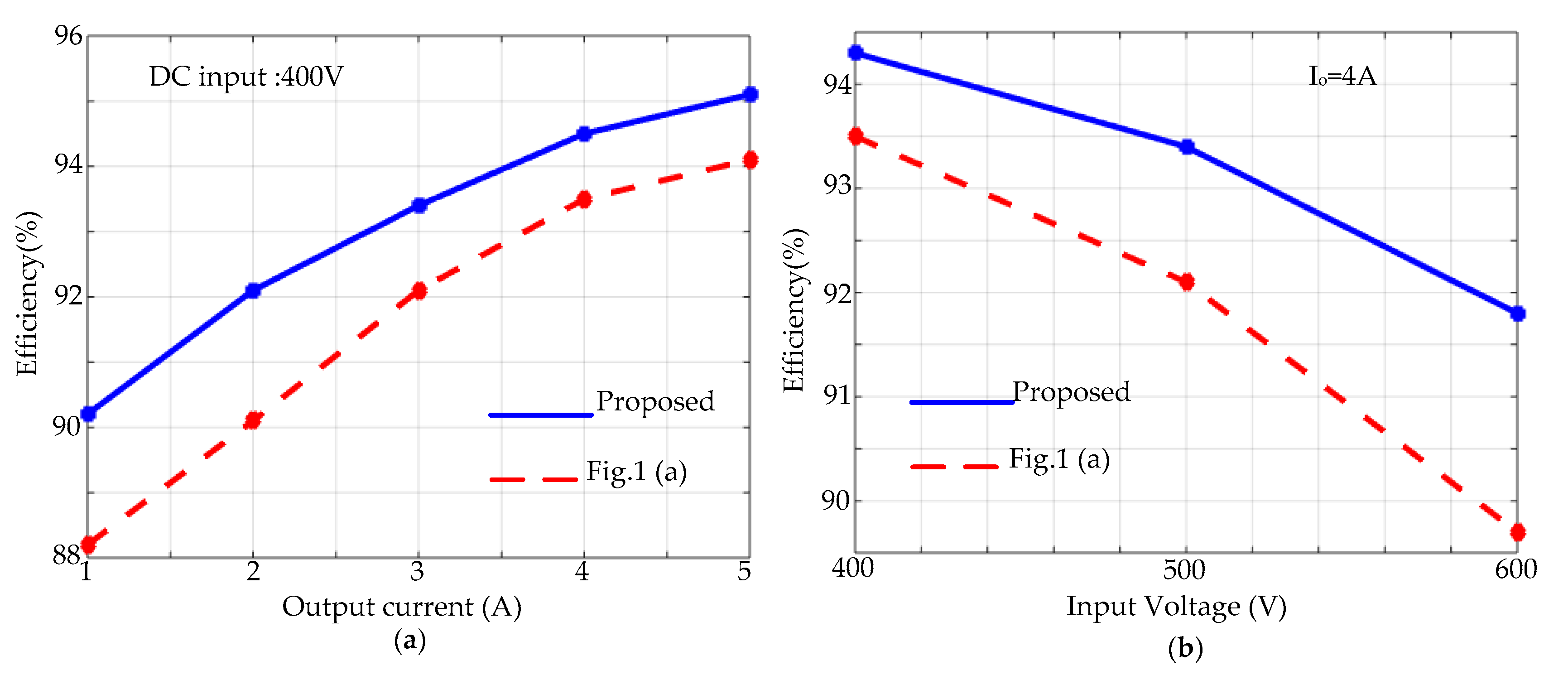
The efficiency comparison results are illustrated in Figure 12. In Figure 12a, the proposed converter has high efficiency under low output current condition owing to reduced switching power loss of the primary switches. Under high output current conditions, the efficiency of the proposed converter is also better due to the fact that switching-off power loss can be further reduced. In Figure 12b, when Io is constant, the efficiency of both converters is changed inversely proportional to Vin. In addition, the efficiency of the proposed converter is decreased slowly owing to the fact that Vin has a small effect on the soft switching condition of the primary switches.
5. Conclusions
A new ZVZCS capacitor-clamped HB TLDC with two unsymmetrical bidirectional switches is proposed and analyzed, and the experimental results can well support the theoretical analysis. After discussion, some obvious advantages of the proposed converter can be concluded, e.g., balanced and reduced current stress of the primary components, small and reduced volume of the clamping capacitor, wide load range soft-switching operation for both turn-on and turn-off instants and a simple switching scheme. The only drawback of the proposed converter is the off voltage of Q3 is slightly higher than Vin/2.
Funding
This research was funded by [Natural Science Foundation of Shaanxi University of Science and Technology] grant number [2016XSGG08].
Conflicts of Interest
The authors declare no conflict of interest.
References
- Pinheiro, J.R.; Barbi, I. The three-level ZVS PWM converter—A new concept in high-voltage DC-to-DC conversion. In Proceedings of the IEEE IECON, San Diego, CA, USA, 13 November 1992; pp. 173–178. [Google Scholar]
- Barbosa, P.M.; Lee, F.C. Design aspects of parallel three-phase DCM boost rectifiers. In Proceedings of the IEEE PESC, Charleston, SC, USA, 1 July 1999; pp. 331–336. [Google Scholar]
- Blaabjerg, F.; Chen, Z.; Kjaer, S.B. Power electronics as efficient interface in dispersed power generation systems. IEEE Trans. Power Electron. 2004, 19, 1184–1194. [Google Scholar] [CrossRef]
- Mohsenian, H.; Davoudi, A. Towards building an optimal demand response framework for DC distribution network. IEEE Trans. Smart Grid 2014, 5, 2626–2634. [Google Scholar] [CrossRef]
- Deschamps, E.; Barbi, I. A comparison among three-level ZVS-PWM isolated DC-to-DC converters. In Proceedings of the IEEE IECON, Aachen, Germany, 31 August–4 September 1998; pp. 1024–1029. [Google Scholar]
- Canales, F.; Barbosa, P.M.; Lee, F.C. A zero-voltage and zero current-switching three level DC/DC converter. IEEE Trans. Power Electron. 2002, 17, 898–904. [Google Scholar] [CrossRef]
- Ruan, X.; Zhou, L.; Yan, Y. Soft-switching PWM three-level converters. IEEE Trans. Power Electron. 2001, 16, 612–622. [Google Scholar] [CrossRef]
- Lin, B. Hybrid DC/DC converter based on dual three-level circuit and half-bridge circuit. IET Power Electron. 2016, 9, 817–824. [Google Scholar] [CrossRef]
- Lin, B.; Zhang, S. Analysis and implementation of a three-level hybrid dc–dc converter with the balanced capacitor voltages. IET Power Electron. 2016, 9, 457–465. [Google Scholar] [CrossRef]
- Lu, S.; Mu, M.; Jiao, Y.; Lee, F.C.; Zhao, Z. Coupled inductors in interleaved multiphase three-level DC–DC converter for high-power applications. IEEE Trans. Power Electron. 2016, 31, 120–134. [Google Scholar] [CrossRef]
- Zhang, Y.; Shi, J.; Zhou, L. Wide input-voltage range boost three-level DC–DC converter with quasi-Z source for fuel cell vehicles. IEEE Trans. Power Electron. 2017, 32, 6728–6738. [Google Scholar] [CrossRef]
- Jin, L.; Duan, S. Comparative analysis of three-level dual active bridge DC–DC converter between reflux-power-optimised and current-stress-optimised phase shift control. IET Power Electron. 2018, 11, 1681–1688. [Google Scholar] [CrossRef]
- Hong, F.; Li, L.; Wu, Y.; Ji, B.; Zhou, Y. 1500 V three-level forward converter with phase-shifted control. IET Power Electron. 2018, 11, 1547–1555. [Google Scholar] [CrossRef]
- Manoranjan, S.; Sivakumar, K. Fault tolerant three-level boost inverter with reduced source and LC count. IET Power Electron. 2018, 11, 399–405. [Google Scholar]
- Ruan, X.; Chen, Z.; Chen, W. Zero-voltage-switching PWM hybrid full-bridge three-level converter. IEEE Trans. Power Electron. 2005, 20, 395–404. [Google Scholar] [CrossRef]
- Ruan, X.; Li, B. Zero-voltage and zero-current-switching PWM hybrid full-bridge three-level converter. IEEE Trans. Ind. Electron. 2005, 52, 213–220. [Google Scholar] [CrossRef]
- Shi, Y.; Wang, X.; Xi, J.; Gui, X.W.; Yang, X. Wide load range ZVZCS three-level DC-DC converter with compact structure. IEEE Trans. Power Electron. 2019, 34, 5032–5037. [Google Scholar] [CrossRef]
- Kim, D.-Y.; Kim, J.-K.; Moon, G.-W. A three-level converter with reduced filter size using two transformers and flying capacitors. IEEE Trans. Power Electron. 2013, 28, 46–53. [Google Scholar] [CrossRef]
- Shi, Y.; Yang, X. Soft switching PWM cascaded three-level combined DC–DC converters with reduced filter size and wide ZVS load range. IEEE Trans. Power Electron. 2015, 30, 6604–6616. [Google Scholar] [CrossRef]
- Shi, Y. Full ZVS load range diode clamped three-level DC–DC converter with secondary modulation. J. Power Electron. 2016, 16, 93–101. [Google Scholar] [CrossRef]
- Liu, D.; Deng, F.; Zhang, Q.; Chen, Z. Zero-voltage switching PWM strategy based capacitor current-balancing control for half-bridge three-level DC/DC converter. IEEE Trans. Power Electron. 2018, 33, 357–369. [Google Scholar] [CrossRef]
- Liu, D.; Deng, F.; Gong, Z.; Chen, Z. Input-parallel output-parallel three-level DC/DC converters with interleaving control strategy for minimizing and balancing capacitor ripple currents. IEEE J. Emerg. Sel. Top. Power Electron. 2017, 5, 1122–1132. [Google Scholar] [CrossRef]
- Liu, W.; Jin, H.; Yao, W.; Lu, Z. An interleaved PWM method with better voltage-balancing ability for half-bridge three-level DC/DC converter. IEEE Trans. Power Electron. 2018, 33, 4594–4598. [Google Scholar] [CrossRef]
Figure 1.
Capacitor-clamped HB TLDC and its key waveforms: (a) Circuit; (b) Key waveforms.
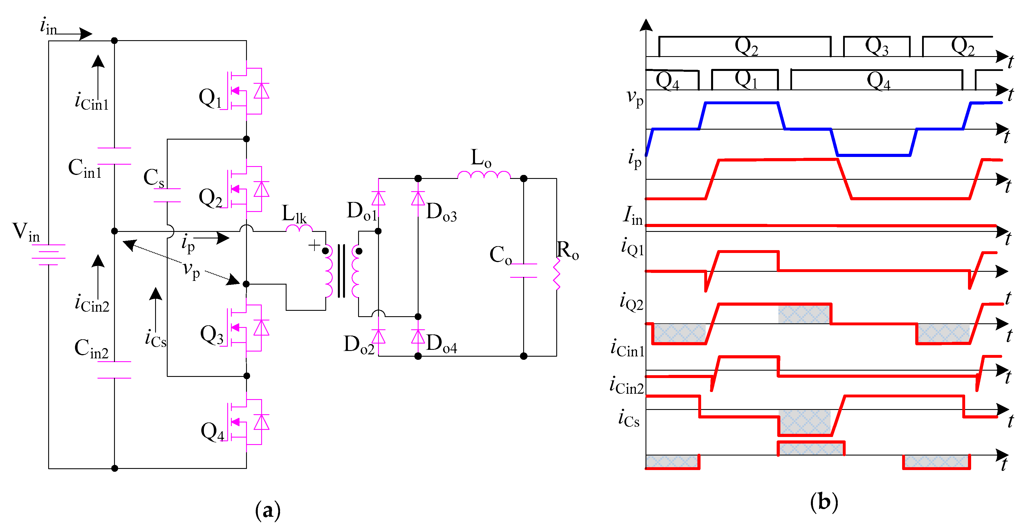
Figure 2.
Proposed capacitor-clamped ZVZCS HB TLDC.

Figure 3.
Key waveforms.
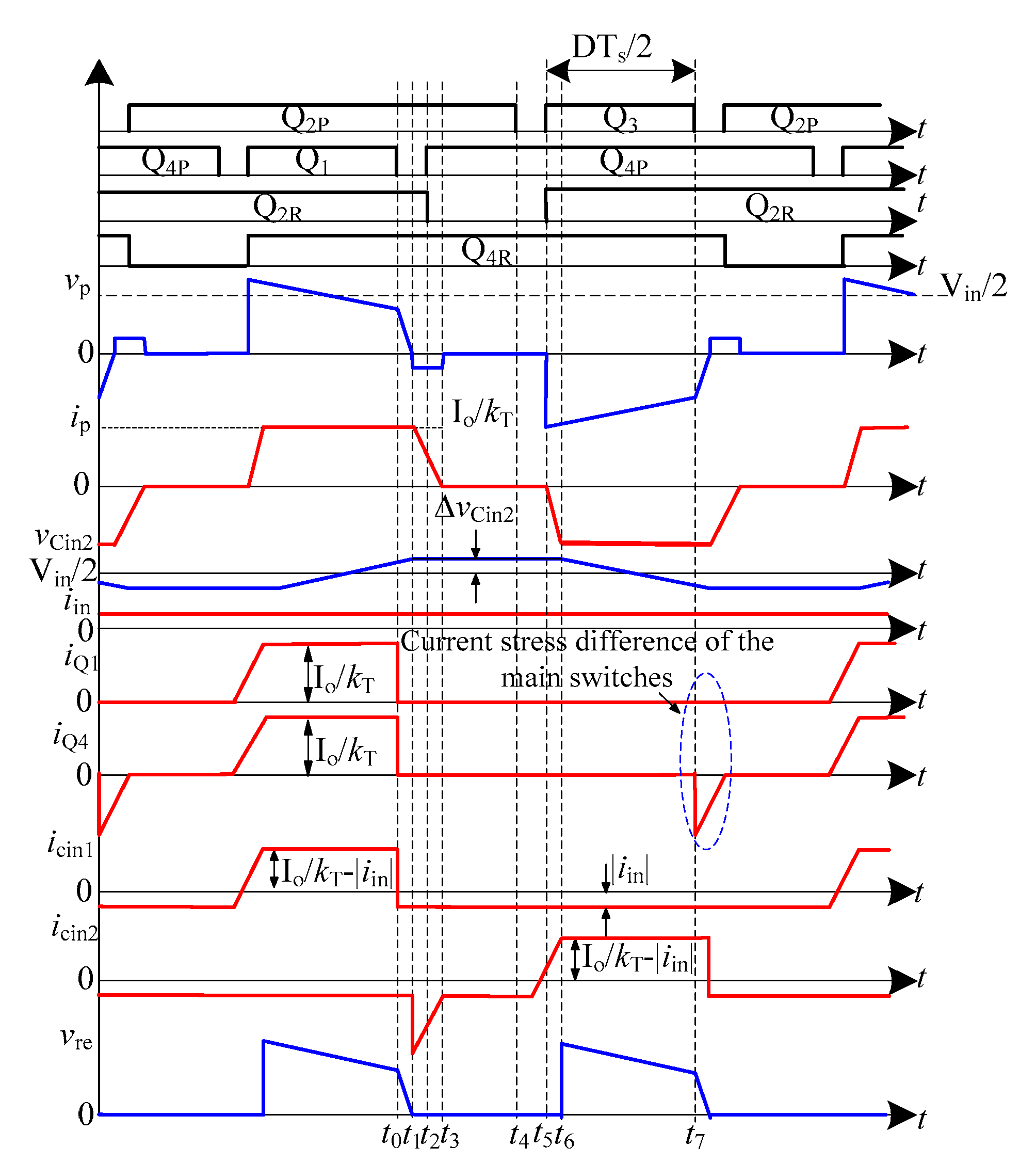
Figure 4.
Identical circuits: (a) Mode 1; (b) Mode 2; (c) Mode 3; (d) Mode 4; (e) Mode 5; (f) Mode 6.
Figure 4.
Identical circuits: (a) Mode 1; (b) Mode 2; (c) Mode 3; (d) Mode 4; (e) Mode 5; (f) Mode 6.
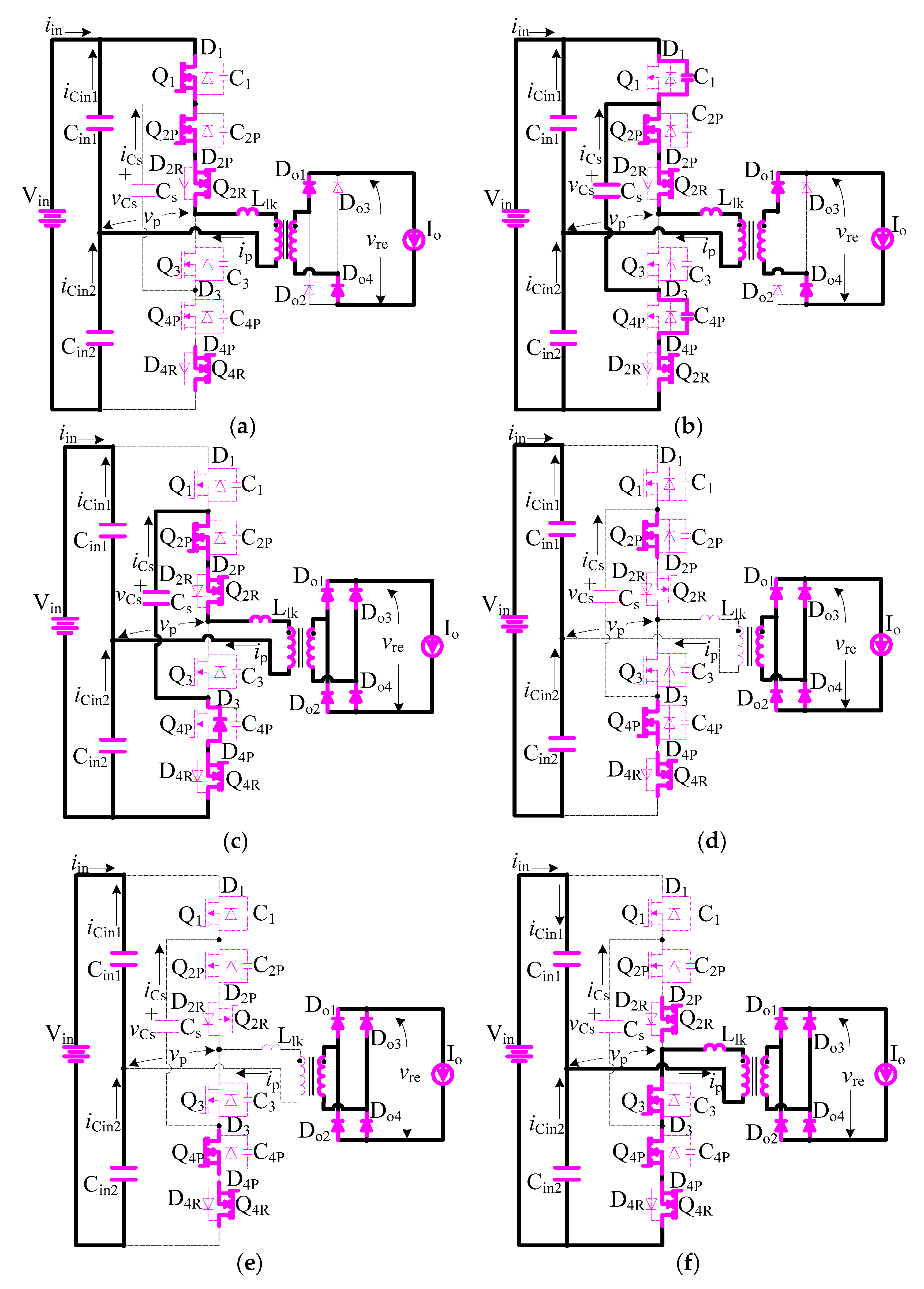
Figure 5.
Current of the primary switches: (a) iQ1 and iQ2 in Figure 1a; (b) iCin1 and iCin2 in Figure 1a; (c) iQ1 and iQ2P in the proposed converter; (d) iCin1 and iCin2 in the proposed converter; (e) iCs.

Figure 6.
Waveform of vp.

Figure 7.
Waveform of ip.
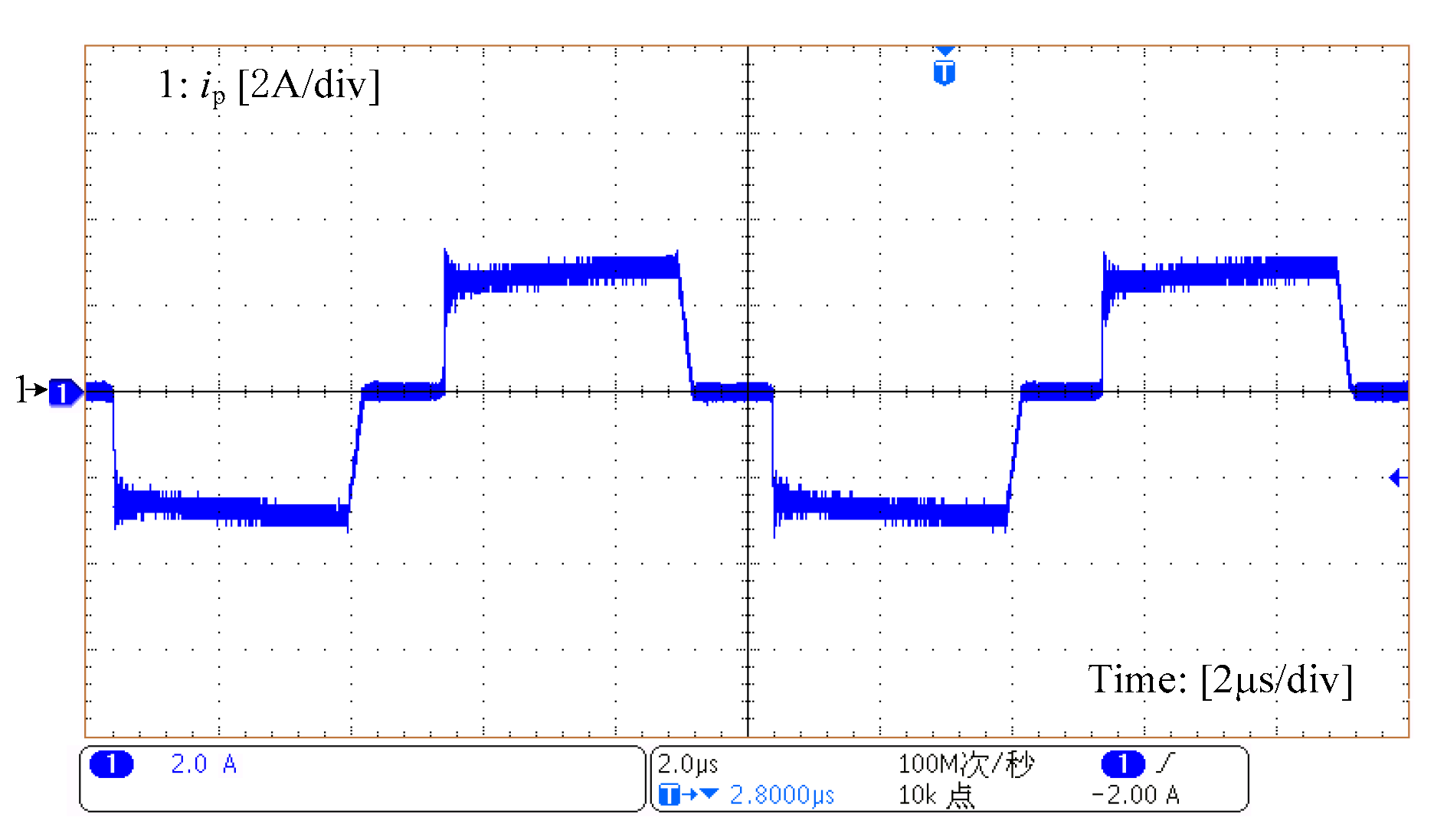
Figure 8.
Waveform of ΔvCin2.

Figure 9.
Waveform of vDo1.
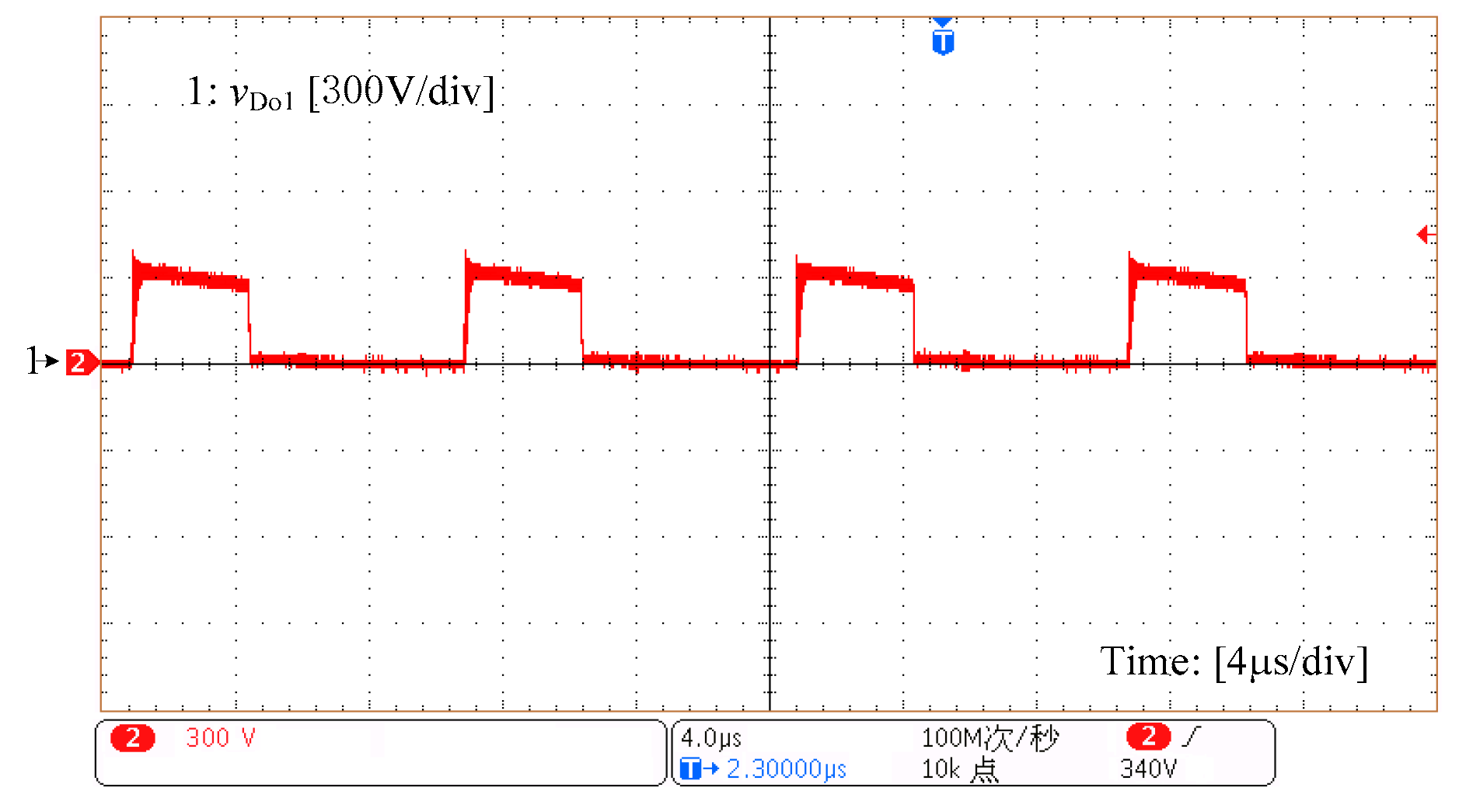
Figure 10.
Waveform of vQ2P and iQ2P.

Figure 11.
Waveform of vQ3, iQ3 and vGSQ3.
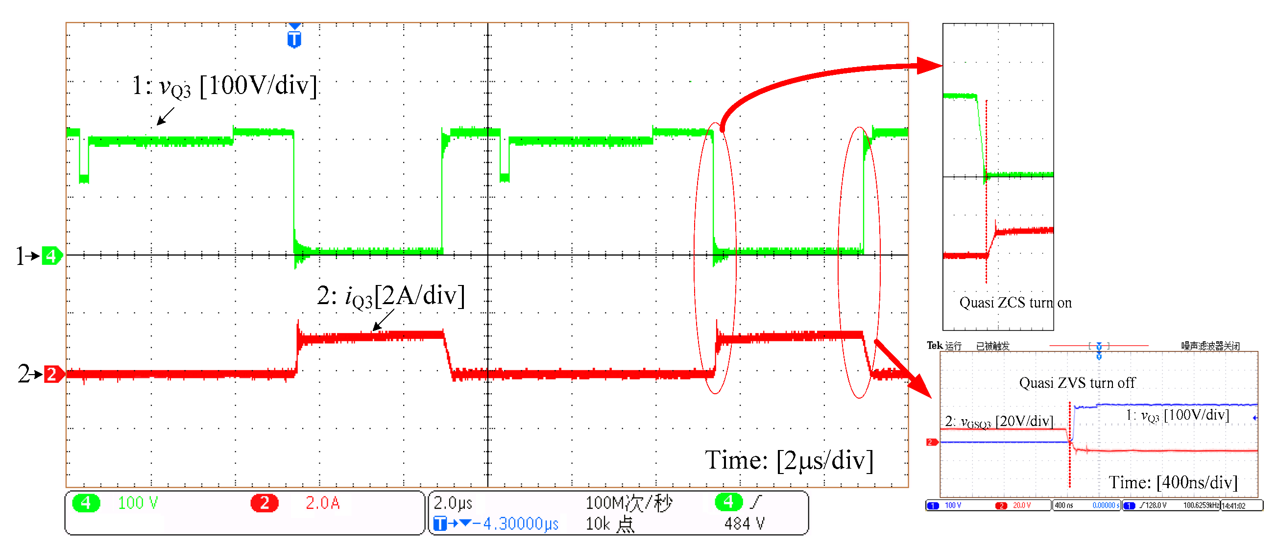
Figure 12.
Efficiency curves: (a) Vin = 400 V, Io is varied; (b) Io = 4 A, Vin is varied.

Table 1.
Soft switching of the main switches.
| Item | Q1 | Q2 | Q3 | Q4 |
|---|---|---|---|---|
| Proposed | ZCZVS, easy | ZVZCS, easy | ZCZVS, easy | ZVZCS, easy |
| Figure 1a | ZVS, hard | ZVS, easy | ZVS, hard | ZVS, easy |
Table 2.
Components comparison.
| Converter | Power Devices High Voltage | Power Devices Low Voltage | Capacitors Large Value | Capacitors Small Value |
|---|---|---|---|---|
| Proposed | 4 | 2 | 0 | 3 |
| [1] | 6 | 0 | 2 | 0 |
| [6] | 6 | 1 | 2 | 1 |
| [7] | 6 | 2 | 2 | 2 |
Table 3.
Performance comparison.
| Converter | Soft Switching Primary Switches | Soft Switching Extra Power Devices | Current Stress Primary Components | Duty Ratio Loss |
|---|---|---|---|---|
| Proposed | Good | Good | Small (even) | Small |
| [1] | Worse | NA | Large (uneven) | Large |
| [6] | Medium | Worse | Small (even) | Small |
| [7] | Medium | Good | Small (even) | Small |
Table 4.
Specifications of the experimental equipment.
| Item | Parameter |
|---|---|
| Vin | 400 V–600 V |
| Rated Vo | 200 V |
| Rated Io | 5 A |
| fs | 100 kHz |
| Q1, Q3, Q2p and Q4p | 20 A/600 V |
| Q2R, Q4R | 20 A/25 V |
| Do1 to Do4 | 20 A/600 V |
| kT | 1:1.15 |
| Cin1, Cin2 | 200 μF |
| Cs | 1.5 μF |
| Lo | 20 μH/5 A |
| Co | 200 μF |
© 2019 by the author. Licensee MDPI, Basel, Switzerland. This article is an open access article distributed under the terms and conditions of the Creative Commons Attribution (CC BY) license (http://creativecommons.org/licenses/by/4.0/).
Share and Cite
MDPI and ACS Style
Shi, Y. Wide Load Range Capacitor Clamped ZVZCS Half Bridge Three-Level DC-DC Converter with Two Unsymmetrical Bi-directional Switches. Energies 2019, 12, 2362. https://doi.org/10.3390/en12122362
AMA Style
Shi Y. Wide Load Range Capacitor Clamped ZVZCS Half Bridge Three-Level DC-DC Converter with Two Unsymmetrical Bi-directional Switches. Energies. 2019; 12(12):2362. https://doi.org/10.3390/en12122362
Chicago/Turabian StyleShi, Yong. 2019. "Wide Load Range Capacitor Clamped ZVZCS Half Bridge Three-Level DC-DC Converter with Two Unsymmetrical Bi-directional Switches" Energies 12, no. 12: 2362. https://doi.org/10.3390/en12122362
Note that from the first issue of 2016, this journal uses article numbers instead of page numbers. See further details here.