Characterization of SiO2/4H-SiC Interfaces in 4H-SiC MOSFETs: A Review


Consiglio Nazionale delle Ricerche–Istituto per la Microelettronica e Microsistemi (CNR-IMM), 95121 Catania, Italy
*
Author to whom correspondence should be addressed.
Energies 2019, 12(12), 2310; https://doi.org/10.3390/en12122310
Submission received: 21 May 2019
/
Revised: 11 June 2019
/
Accepted: 12 June 2019
/
Published: 17 June 2019
(This article belongs to the Special Issue Volume II: Semiconductor Power Devices)
Abstract
:This paper gives an overview on some state-of-the-art characterization methods of SiO2/4H-SiC interfaces in metal oxide semiconductor field effect transistors (MOSFETs). In particular, the work compares the benefits and drawbacks of different techniques to assess the physical parameters describing the electronic properties and the current transport at the SiO2/SiC interfaces (interface states, channel mobility, trapping phenomena, etc.). First, the most common electrical characterization techniques of SiO2/SiC interfaces are presented (e.g., capacitance- and current-voltage techniques, transient capacitance, and current measurements). Then, examples of electrical characterizations at the nanoscale (by scanning probe microscopy techniques) are given, to get insights on the homogeneity of the SiO2/SiC interface and the local interfacial doping effects occurring upon annealing. The trapping effects occurring in SiO2/4H-SiC MOS systems are elucidated using advanced capacitance and current measurements as a function of time. In particular, these measurements give information on the density (~1011 cm−2) of near interface oxide traps (NIOTs) present inside the SiO2 layer and their position with respect to the interface with SiC (at about 1–2 nm). Finally, it will be shown that a comparison of the electrical data with advanced structural and chemical characterization methods makes it possible to ascribe the NIOTs to the presence of a sub-stoichiometric SiOx layer at the interface.
1. Introduction
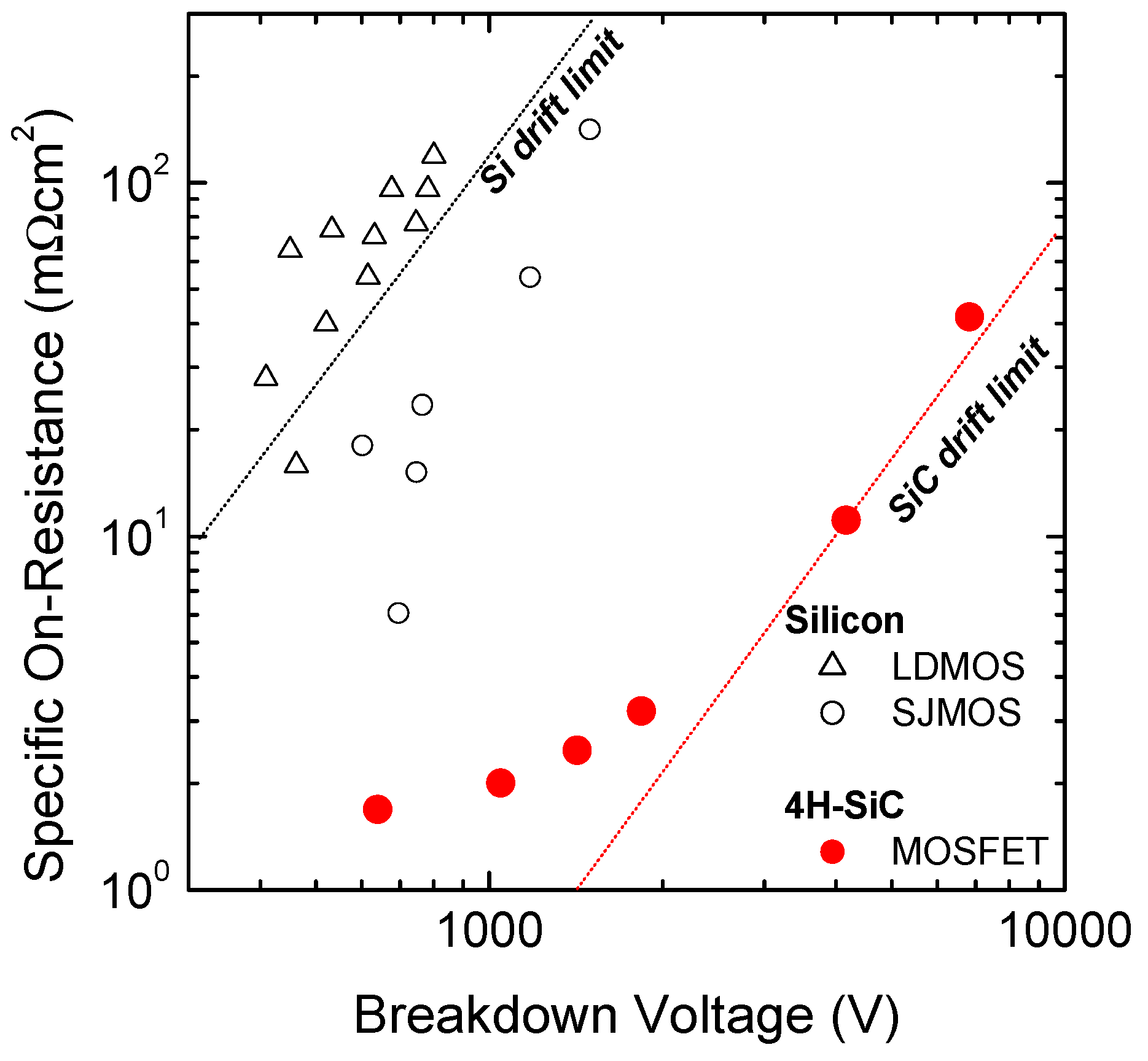
Silicon carbide (4H-SiC) is the best candidate to replace silicon in power electronics applications. In particular, its high critical electric field and large band gap make it possible to design devices with a high breakdown voltage (BV), having specific on-resistance (Ron,sp) two orders of magnitude lower than silicon-powered devices. This concept is clearly illustrated in the Ron,sp versus BV plot depicted in Figure 1.
The Ron,sp versus BV plot shows that planar metal oxide semiconductor field effect transistors (MOSFETs) have approached the 4H-SiC unipolar limit for BV values larger than 1200 V. However, both the commercial and the R&D devices designed for operating in the 600–900 V range [1,2] are still far from the ideal unipolar limit. This behavior can be explained by looking at the structure of the planar power MOSFETs and at the SiO2/SiC interface.
Figure 2 shows the schematic cross section of the elementary cell of the planar power MOSFETs, indicating also the vertical current path connecting source to drain electrodes in the on-state and each resistance components. As can be seen, the total Ron,sp of the device can be written as the sum of different contributions [3]:
where Rch is the channel resistance, Ra is the accumulation (between the n-type epitaxy and the insulator) region resistance, RJFET is the resistance of the JFET (junction Field-Effect Transistor) region (from the surface to the end of the body region), Rdrift is the resistance of the drift region after taking into account current spreading from the JFET region (from the body region to the end of the epitaxial layer), and Rsub is the resistance of the n-type doped substrate.
While Ra and RJFET can be minimized by appropriately scaling the device layout, and Rsub can be reduced by thinning the substrate, the control of the channel resistance contribution Rch is more critical. In fact, the channel resistance contribution Rch is given by [3]:
where p is the pitch of the MOSFET elementary cell, Lch is the channel length, µinv is the mobility for electrons in the channel (inversion layer), Cox is the specific capacitance of the gate oxide, Vth is the threshold voltage, and VG is the applied gate bias. It is important to emphasize that power devices must have a good trade-off between the ON- and OFF-state. In particular, for a given breakdown voltage and threshold voltage, the choice of a drift layer and body region with fixed doping levels and thicknesses are required. Hence, the minimum pitch size is obtained, avoiding the overlap of the depleted region of the body-drain p-n diode (in the JFET region). Furthermore, the Rch can be influenced by the Cox. However, to guarantee the reliability of power devices, insulators with high critical breakdown field, large band gap, and high melting point are desired. So far, the most robust gate insulation solution is the SiO2, but recent literature is exploring alternative solutions, such as Al2O3 [4] and AlON [5]. Moreover, the channel resistance Rch can be lowered by reducing the channel length. However, when the MOSFET operates in interdiction and it is reverse biased, short-channel phenomena have to be avoided. Hence, the reduction of Rch is strictly related to the optimization of the inversion channel mobility µinv. This optimization clearly requires a good comprehension of the physical phenomena governing the transport in the channel. In addition, besides the inversion channel mobility µinv, the threshold voltage Vth is another important parameter, which directly influences the channel resistance. Hence, channel mobility and threshold voltage must be accurately controlled to optimize the device performance and to fully exploit the benefits of the 4H-SiC material.
Several review papers recently reported on the physical and technological issues which limit the performances and reliability of 4H-SiC MOSFETs in power electronics applications [6,7,8]. In general, 4H-SiC MOSFETs are characterized by a low inversion channel mobility and the occurrence of Vth instability phenomena under bias stress [9,10]. The Vth stability is a very important request, to avoid degradation and/or irreversible device failure under long time stress condition at temperatures above 150 °C.
The SiO2/4H-SiC metal-oxide-semiconductor (MOS) system is the most important part of the transistor, and it is schematically depicted in Figure 3. Clearly, the behavior of the SiC power MOSFET depends critically on the properties of the SiO2/4H-SiC MOS system. In particular, some relevant regions can be identified in the SiO2/4H-SiC MOS system. The first one is the SiO2/4H-SiC interface, which is characterized by the presence of a distribution of interface states (Dit), close either to the valence or conduction band edge [11,12]. Then, a second region inside the gate insulator is characterized by the presence of slow near interface oxide traps (NIOTs) and bulk traps [13,14]. Finally, a “modified” 4H-SiC region close to the interface with SiO2 is typically present in the MOS system. This latter region may be different under the electrical or structural/chemical point of view with respect to the bulk 4H-SiC semiconductor [15].
Clearly, in such a complex scenario, only the cross correlation of a variety of characterization techniques can make it possible to obtain an exhaustive picture of the SiO2/SiC interface and, hence, to provide useful feedback for the 4H-SiC MOSFET manufacturers.
The goal of this paper is to give an overview of the current issues related to the characterization of SiO2/4H-SiC interfaces. In particular, the importance of correlating conventional electrical analyses of devices and test patterns, with more advanced characterization techniques at the nanoscale, is highlighted. As an example, it will be shown that using nanoscale approaches can make it possible to get insights on the spatial homogeneity of the surface potential at the SiO2/4H-SiC interface and explain the deviations from the ideal behaviour. Finally, the relevance of time-resolved measurements to study trapping states at the SiO2/4H-SiC interface will be also emphasized.
2. Interface States Density and Channel Mobility in 4H-SiC MOS-Based Devices
In general, the parameter used to describe the channel behaviour in 4H-SiC MOSFETs is the field effect mobility, μFE, determined from the device transconductance in the linear region according to equation:
where W is the channel width, VDS is the source-drain potential, and is the MOSFET transconductance. The field effect mobility contains the physical information on the modulation of the channel conductivity by the application of the gate bias. Typically, μFE is determined in lateral MOSFETs, i.e., where the device resistance is given only by the contacts and the channel contributions. In fact, in a lateral MOSFET, the JFET, accumulation, and drift resistance contributions are absent.
The SiO2/4H-SiC interface is characterized by the presence of a relatively high density of interface states Dit (> 1012 eV−1cm−2) close to the conduction band edge. It is widely accepted that the presence of a large amount of interface states Dit is detrimental for the field effect mobility µFE and on-resistance RON of 4H-SiC MOSFETs [7,16]. According to the studies reported in the last decades, the µFE can be improved with different passivation processes of the SiO2/SiC. The passivation can be achieved by thermal annealing in nitrogen-rich atmospheres (NO or N2O) [17,18,19,20]. Table 1 compares several literature data concerning the channel mobility measured in 4H-SiC MOSFETs, fabricated either on epitaxial or ion-implanted layers, or MOS capacitors, and subjected to annealing of the gate oxides in nitrogen-rich conditions or combined oxidation (including high temperature Argon annealing) [21,22,23,24,25,26,27,28,29,30] that reduced the Dit amount. Typically, the passivation annealing temperatures are in the range 1100–1400 °C. As can be seen, a notable increase of the channel mobility (up to 20–50 cm2V−1s−1) can be achieved upon nitridations of the gate oxide, with respect to the values typically measured in non-annealed thermal oxides (typically below 5 cm2V−1s−1) [19]. The improvement of the channel mobility is often, but not always, accompanied by a reduction of the interface state density Dit (down to the low 1012 eV−1cm−2 range). It is assumed that the passivation mechanism of SiO2/4H-SiC interface consists in the elimination of an excess of carbon at the interface or in the saturation of dangling bonds [31].
Rozen et al. [28] reported a correlation between the MOSFET channel mobility, the amount of nitrogen incorporated at the SiO2/4H-SiC interface upon annealing in NO, and the interface charged states Nit (the integral of Dit over the gap). Besides the NO or N2O post-annealing treatments, other processes can be beneficial for Dit and/or µFE. As an example, Kobayashi et al. [32] reported that a high temperature annealing (up to 1500 °C) in Ar can improve the SiO2/4H-SiC interface, by avoiding the formation of fast states still present after NO or N2O processes. Hatakeyama et al. [33] showed a dependence of the Dit on the annealing time in NO at 1250 °C, obtaining the best mobility results after 60 min annealing. More recently, Asaba et al. [34] combined a low temperature (900 °C) annealing in O2 to promote the subsequent Nitrogen incorporation at the interface with a N2 annealing at 1300 °C, reaching a field effect mobility of 50 cm2V−1s−1.
It is clear from the data collected in Table 1 that a correlation between the channel mobility µFE and the Dit is not straightforward, because the µFE and Dit are typically determined using different techniques (high-low method, conductance method Gp/ω, C–ψ method, etc.). Table 2 and Table 3 summarize the most widely used characterization techniques to determine channel mobility and interface states, illustrating their advantages and limitations.
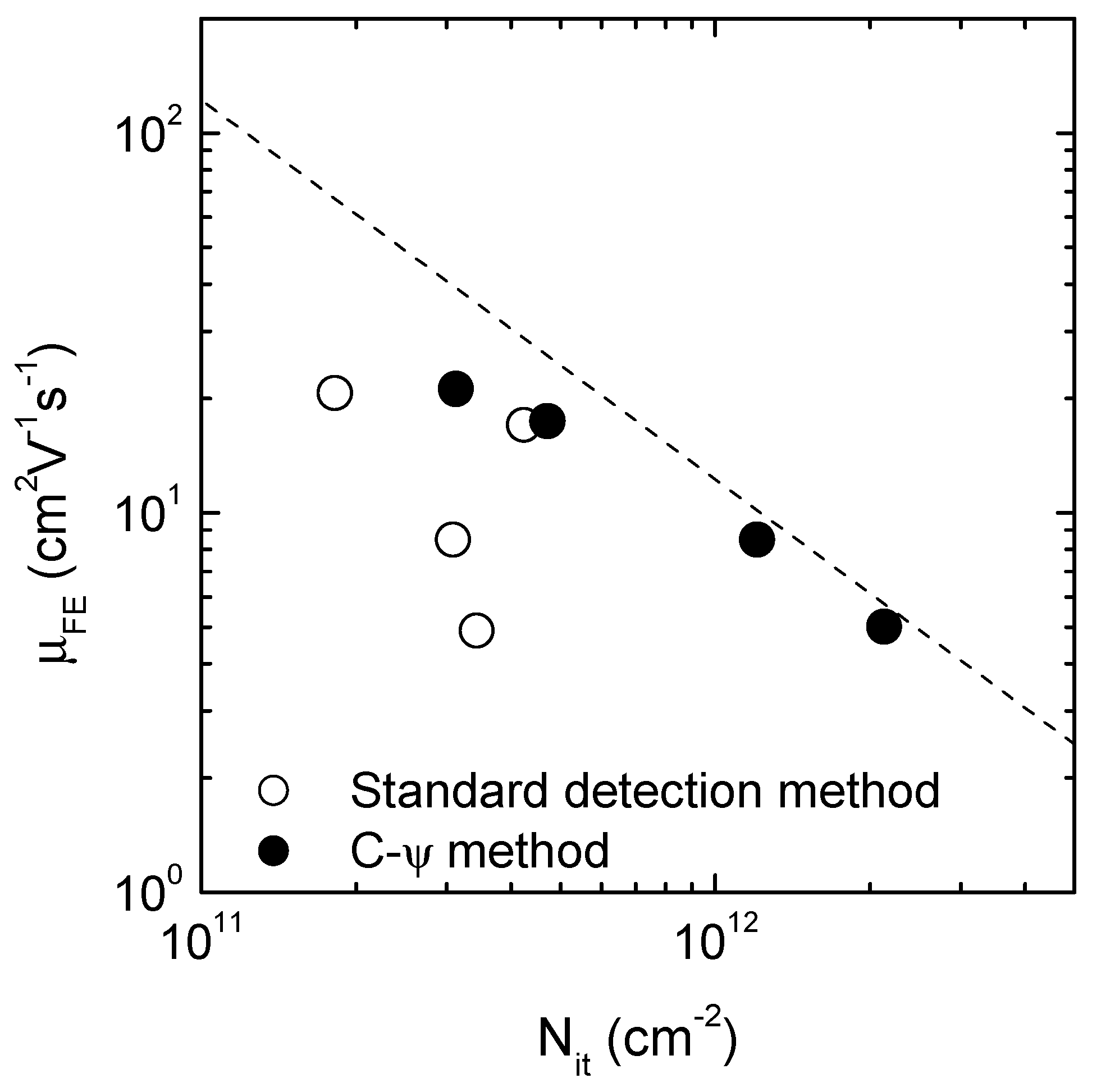
The conventional characterization methods used to determine the Dit at SiO2/4H-SiC interfaces are the high-low method [35] and the frequency dependent parallel conductance measurements (Gp/ω or conductance method). The high-low method compares a low-frequency C–V curve with a high-frequency C–V curve. The high frequency C–V curve is acquired at a frequency (e.g., 1 MHz) where the interface traps are supposed to not respond to the AC signal. Low frequency means that interface traps and minority carrier inversion charges should respond to the measurement AC probe frequency. Unfortunately, standard C–V performed at 1 MHz on 4H-SiC do not fully satisfy this condition. On the other hand, the Gp/ω (or conductance method) is sensitive to Dit in the portion of the band gap that corresponds to depletion and weak inversion, and also the capture cross-sections for majority carriers, and surface potential fluctuations. The Gp/ω method measures the equivalent parallel conductance Gp of an MOS capacitor as a function of frequency and bias. However, in SiO2/4H-SiC interfaces there is a non-negligible amount of Dit above the Fermi level, where the Gp/ω method is not sensitive. Hence, the abovementioned techniques underestimate the distribution of Dit when q2·Dit > Cox [36]. Furthermore, the Gp/ω method is not sensitive to the fast states that can be undetectable in the usually employed frequency range (up to a few MHz; see Table 2) [16]. Thus, in order to detect the fast states, Yoshioka et al. [37] proposed a novel method based on the difference between the theoretical and quasi-static capacitances in SiC MOS capacitors (C–ψ). In fact, by employing the C–ψ method, it was possible to make a correct determination of the Dit and, hence, to establish a correlation between the Dit and the field effect mobility µFE. [38], as shown in Figure 5.
Another characterization technique, the charge pumping method, commonly used in silicon devices [39], is recently rising relevance also for SiC devices. This method is based on measuring the transistor base charge-pumping current while applying voltage pulses (variable amplitudes and lengths) to its gate. In particular, the difficulty in interpreting anomalous data collected on 4H-SiC MOSFETs has been firstly explained by Okamoto et al [40] in terms of geometric components and the acceptor-like interface states. In fact, due to the low channel mobility, the charge carriers need a certain time to cross the channel. Hence, an accurate setting of the experimental procedure is needed. More recently, Salinaro et al. [41] found an appropriate temperature, frequency, and bias amplitude to demonstrate not only the interface state distribution but also a not homogeneous doping distribution in the channel due to the device processing.
Although the 4H-SiC MOSFET mobility is often determined from Equation (3), this approach would give the correct channel mobility value only in the absence of charge trapping effects. In fact, under this assumption, the total density of free electrons nfree contributing to the channel conduction corresponds to the total inversion layer electrons density nTOT (nfree = nTOT). However, in the presence of electron trapping at interface states, a substantial fraction of the inversion layer electrons is trapped (nfree < nTOT) [42]. Hence, using the device transconductance (from the current-voltage characteristics) leads to an underestimation of the actual channel mobility.
On the other hand, the effective mobility, μeff, is extracted from the device conductance in the linear region (typically at VDS = 50–100 mV), according to the equation:
where Qn is charge density the channel (C/cm2).
However, the measure of μeff presents some weaknesses. First, the effective charge in the inversion layer Qn = Cox(VGS − Vth) is difficult to measure accurately. In fact, to accurately determine the Qn, complicated experimental setups are needed in order to perform the split C–V measurements [35] separating the source-drain and gate-base capacitance response. Second, the additional series capacitances introduced by the interface states can influence the mobility estimation.
Generally, in 4H-SiC MOSFETs, the value of the effective mobility μeff is lower than the field effect mobility μFE. This discrepancy is due mainly to the presence of interface traps affecting the explicit Qn dependence of µeff (µFE is not explicitly related to Qn) but not draining conductance or draining current. In fact, Qn is the sum nfree + nTrap. Since nTrap is not contributing to the channel conduction, Qn is larger than nfree, thus resulting in a considerable underestimation of µeff (< µFE).
A different way to characterize the properties of the MOSFET channel is determining the Hall Effect Mobility, μHall. In fact, the Hall measurement gives a direct measurement of the free electrons nfree. Hence, the big advantage of the Hall measurement is that μHall and nfree are determined independently. Consequently, the technique provides correct mobility results, independent of the charge trapping [42]. On the other hand, the total amount of charge at each gate bias value—or, alternatively, at each surface potential value—aligns with Qn =Cox(VGS−Vth) and this allows the extraction of the interface states profile. The values of the Hall mobility are higher than the field effective mobility. Obviously, for Hall measurements, special test patterns must be designed (i.e., Hall bars in the MOSFET channel). Moreover, the accurateness of this method is correlated to the knowledge of the Hall scattering factor [43]. Recently, Hall measurements have been used by Hatakeyama et al. [33] to determine the total amount of the trapped and free carriers in the channel of 4H-SiC MOSFETs subjected to different NO treatments, and their results are reported in Table 1. They have demonstrated that the improvement of the Dit and of the Hall mobility is not strictly related to the duration of the NO treatments. In fact, a post-oxidation-annealing (POA) duration that exceeds a certain time can produce a detrimental effect compared with a shorter POA duration.
After the mentioned clarifications on the experimental methods to determine both the interface state density and the MOSFET channel mobility, it is possible to try to draw a correlation between the µFE and the Dit.
Figure 4 shows the data obtained from Nakazawa et al. [38] correlating the µFE and the total amount of the interface states Nit (the energy integral of the Dit). As can be seen, unlike the conventional characterization methods (e.g., 1 MHz conductance method and high-low), a nice correlation of the peak mobility µFE with the reverse of the interface trap density (1/Nit) is visible when the C-ψ method is used for the quantification of Dit. Clearly, the values of the mobility increase, decreasing the amount of Nit. The mentioned dependence is a strong indication that a Coulomb-scattering contributes to limiting the carriers transport at the SiO2/SiC interface [29].
Very recently, Hauck et al. [44] presented an analytical method that overcomes some of the limits of many methodologies originally developed for silicon devices. In particular, their analytical model makes it possible to correct the underestimation of the charge carrier concentration and mobility. The method provides a formulation of the three-terminal 4H-SiC MOSFETs characterization of any geometry, consisting of an accurate determination of device parameters hampered by the presence of traps at the interface. They parametrized the SiC/SiO2-specific interface trap spectrum, including the body of known data. The resulting parameters, such as the mobility, the charge carrier density, and threshold voltage, have been demonstrated to be in good agreement with Hall effect measurements.
Clearly, the characterization of interface states at SiO2/4H-SiC interfaces is continuously an object of scientific debate. In this context, to overcome some limitations of the conventional electrical characterization techniques, the cross correlation with nanoscale electrical characterization techniques is mandatory to obtain a better view of the SiO2/SiC interface physics.
3. Nanoscale Electrical Properties of SiO2/4H-SiC Interfaces
3.1. Electrical Characterization
The electrical behaviour of 4H-SiC MOSFETs is affected by the microscopic nature of the SiO2/SiC inversion channel. As an example, the roughness of the channel region, often characterized by a typical “step bunching” of the surface, can have an impact on both the interface state and mobility of the fabricated devices.
In this context, some authors reported on an anisotropy of the channel mobility µFE in 4H-SiC MOSFETs, with the channel in different orientations [30,45]. In particular, 4H-SiC MOSFETs fabricated with the channel along the [1–100] direction (along the bunched steps) exhibited a higher channel mobility compared to those fabricated with channel along the [11–20] direction (across the bunched steps) [45]. Frazzetto et al. [29] explained this effect, taking into consideration the impact of both Dit and surface roughness in the scattering contributions to the field effect mobility. However, the conventional device electrical characterization methods were not able to give an exhaustive picture of the involved physical phenomena.
Hence, in recent years, strong efforts have been devoted to an accurate characterization of SiO2/4H-SiC interfaces, employing nanoscale electrical/structural analyses of the interface (e.g., scanning probe microscopy, transmission electron microscopy).
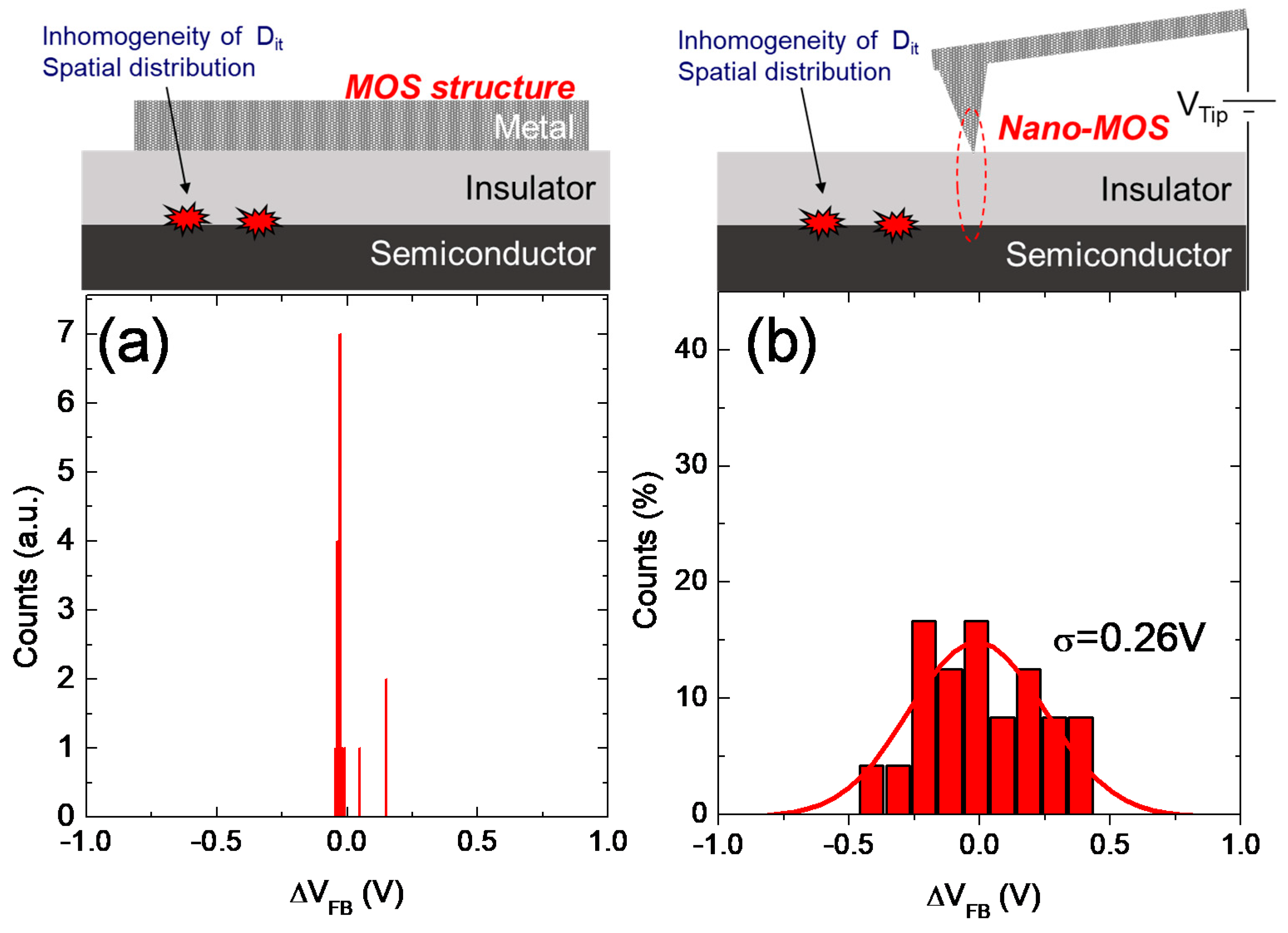
As an example, Figure 5 compares the dispersion of the flat band voltage ΔVFB measured both by conventional C–V measurements and by scanning capacitance microscopy (SCM).
As can be seen (Figure 5a), the C–V characterization of 25 large area state-of-the-art (N2O annealed) MOS capacitors (i.e., 100 × 100 μm2) gives a narrow dispersion of the flat band voltage, indicating a homogeneous SiO2/4H-SiC interface behaviour. Interestingly, nanoscale electrical measurements can provide information that cannot be assessed using macroscopic MOS capacitors. The SCM measures the capacitance variations (dC/dV) produced by the modulating bias at each atomic force microscope (AFM) tip position [30]. The SCM tip is scanned in contact mode on the bare surface of a semiconductor (e.g., 4H-SiC) coated by an insulating film (e.g., SiO2), thus forming a nanometric tip-insulator-semiconductor (nanoMOS) device. The sample is biased by a DC bias and a high frequency (between 10 and 100 kHz) AC bias. The capacitance sensor connected to the probe detects the capacitance variations induced by the modulating AC bias in the tip-insulator-semiconductor (nanoMOS) structure. Due to the nanometric contact size, the capacitance of the tip-insulator-semiconductor nanoMIS structure is extremely small, to the order of ~10−18 F (aF). To disentangle this small capacitance signal from the large stray capacitance values (associated with the cantilever, wires, etc.), a lock-in amplifier connected to the capacitance sensor selects the capacitance contributions at the AC bias modulating frequency. As a result, the lock-in amplifier output is an arbitrary unit signal proportional to the differential capacitance (dC/dV) of the nanoMOS system. As matter of fact, the dC/dV peak values are primarily related to the local flat band voltage in the region underneath the tip. Hence, the spatial variation of the dC/dV peak positions can be correlated to VFB dispersion.
Figure 5b shows the VFB dispersion obtained by the dC/dV SCM signal collected at 25 points—a matrix 5 × 5 at 1 µm distance in the XY directions—on the same sample. Evidently, the VFB dispersion collected at nanoscale (Figure 5b) is broader than that collected on macroscopic capacitors (Figure 5a), thus suggesting the presence of a non-homogeneous Dit distribution.
A possible origin of the non-homogeneous distribution of the electrical properties of the SiO2/4H-SiC interface can be identified by comparing the spatial distribution of the capacitance signal collected using the SCM.
Figure 6a,b show the morphology and the capacitance maps collected on the bare surface of a nitridated SiO2/4H-SiC sample at 1150 °C in N2O. The non-uniform spatial distribution of the capacitance signal can be associated with the spatial fluctuation of the surface potential. For example, in a faceted surface, the non-uniform Dit spatial distribution is correlated with [46] the different contributions to the total Dit value given by the (11−2n) planes of the surface facets and the (0001) basal planes [47]. Saitoh et al. [48] reported on the variation in the density of the interface states in MOS capacitors fabricated on 4H-SiC with different miscut angles, moving from 8°, i.e., the (0001) largest basal plane, up to 90° toward the [11−20] direction, i.e., the (11−20) plane.
The non-uniform spatial distribution of the interface states can be either intrinsic properties of the material—i.e., due to the different local electronic structure of the 4H-SiC crystallographic orientations—or related to a different incorporation of nitrogen during the post oxidation annealing. This aspect will be discussed more in detail in the following section.
3.2. Effects of Counter Doping and Interface Stress
As specified in Section 2, in order to improve the channel mobility in SiO2/4H-SiC MOS-based devices, post-deposition (PDA) or post-oxidation annealing (POA) processes of the gate oxide in N2O or NO are employed. During these nitridation annealings, nitrogen can diffuse through the oxide and reach the SiO2/4H-SiC interface, where it passivates the interface states. For long time, nitrogen was believed to determine only the electrical passivation of the interface states Dit. However, in 2011 Umeda et al. [15] and Kosugi et al. [49] suggested that nitrogen atoms are also incorporated in the crystalline structure of the 4H-SiC substrate, introducing shallow donor levels responsible for the increased conductivity of the MOSFET channel upon nitridation. These works used low temperature (20 K) electrically detected magnetic resonance (EDMR) to separate the effects of the nitrogen interface incorporation, i.e., interface state density reduction and dopant incorporation.
Later, Swanson et al. [50], using scanning spreading resistance microscopy (SSRM), was able to demonstrate that the nitridation process induces a “counter doping” effect of nitrogen in the p-type body region of a MOSFET. This effect has been quantified by Fiorenza et al. [51], by means of cross sectional scanning capacitance microscopy (SCM) measurements on the SiO2/4H-SiC interface. In particular, SCM in cross sections showed that the faceted 4H-SiC surface morphology incorporates a larger nitrogen amount compared to the basal planes, because it exposes different ratios between (0001) and (11−20) planes [47]. Other studies based on transmission electron microscopy (TEM) [52,53] and X-ray photoemission spectroscopy (XPS) [49] demonstrated that nitrogen is incorporated within a couple of 4H-SiC crystalline monolayers.
The correlation of SCM and SSRM analyses in cross sectional samples exposed to different post oxidation annealing allowed the quantification of the counter doping effect and to evaluate the thickness of the electrically modified region underneath the SiO2/4H-SiC interface. In fact, the SCM is able to quantify the doping by the comparison of the known signal collected on the epitaxial layer and on the substrate bulk [54]. On the other hand, SSRM is able to measure the local spreading resistance that is proportional to the local resistivity. Hence, SSRM is not affected by any profile broadening due to the typical depletion contribution in capacitance-based measurements (SCM).
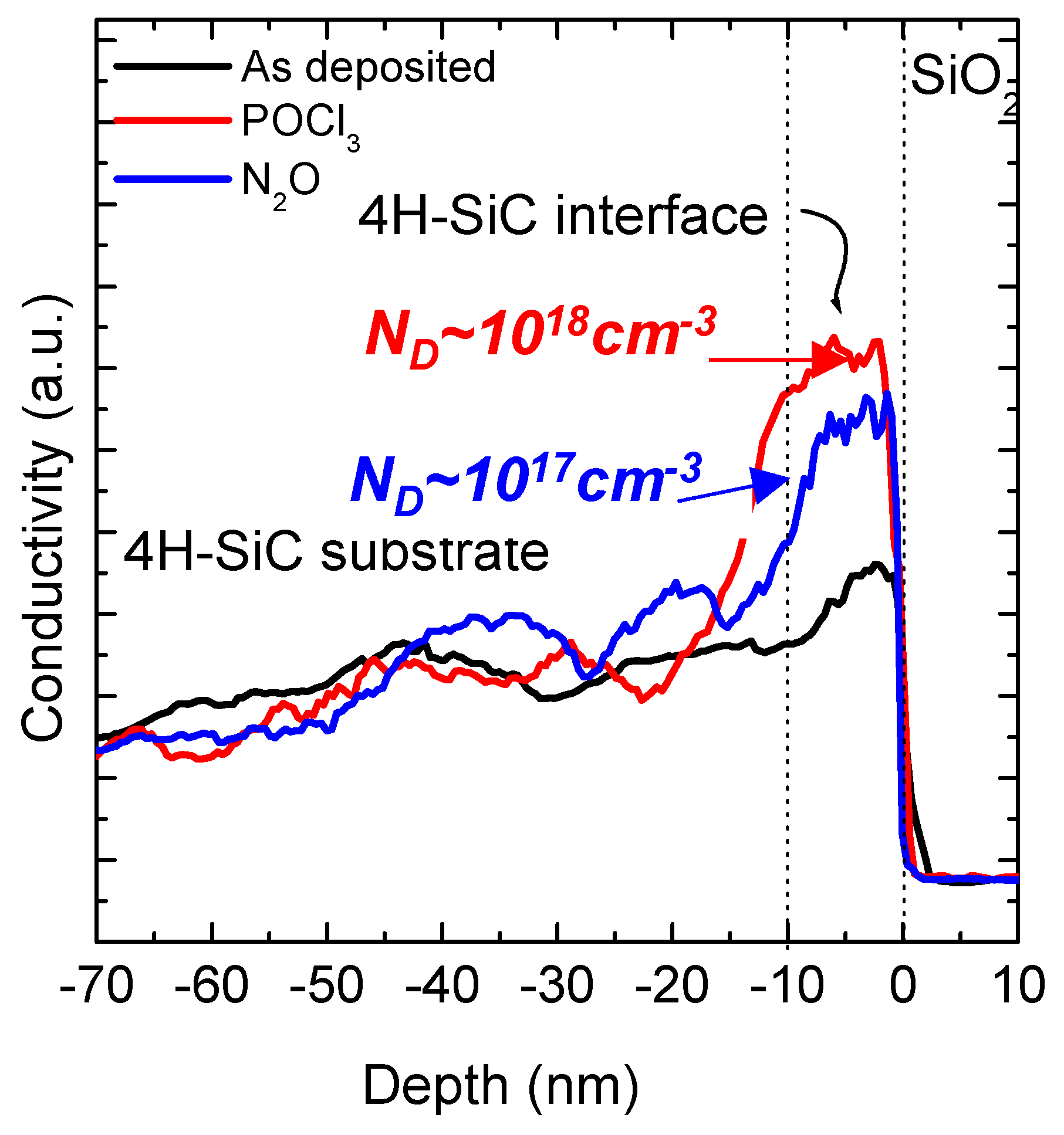
Figure 7 shows the comparison between the conductivity profile on the as deposited (black line) and N2O annealed (blue line) samples, determined using the SSRM. Fabrication details can be found in Reference [55]. As can be seen, the number of free carriers in the nitridated sample is increased by more than one order of magnitude in a region about 10 nm wide from the SiO2/4H-SiC interface [47,51]. Thus, it can be concluded that the nitridation process modifies only a small fraction of the 4H-SiC crystal (one-two monolayers) but it increases the free carrier concentration in the MOSFET inversion region, effectively reducing the channel resistivity. The free carrier profile is locally increased from the doping level of the epilayer (1016 cm−3) to ~1017 cm−3, due to the nitrogen electrically active incorporation.
However, nitridation is not the only process inducing a counter doping effect. In fact, several processes have been reported in the last decade which improve the MOSFET channel resistivity. Some of them are based on the incorporation of elements of the V group of the periodic table, P [51,56,57,58], Sb [59], As [60], which can produce a counter doping effect similar to N atoms. As an example, Figure 7 shows also the free carrier profile on the POCl3 annealed (red line) sample, collected using the SSRM. In this case, the free carrier concentration is locally increased up to ~1018 cm−3, thus demonstrating a higher counter doping effect induced by phosphorous compared to nitrogen.
On the other hand, the incorporation of elements of the II and III groups of the periodic table, B [7,44], Ba [45], Ca [60], La [54], Sr [60], has been investigated to explore other possible effects that explain the increase of MOSFET channel mobility. In fact, elements of the II and III groups cannot provide donors in the channel region, similar to the V group elements. The improvement of the MOSFET field effect mobility (see Table 4) induced by the use of such gate oxide process (e.g., B, Ba, Ca, Sr, or Sb at the interface) could be clarified using advanced TEM analyses, and was attributed to strain relaxation of the SiO2/4H-SiC interfaces [61,62].
SiO2 and 4H-SiC have different thermal properties and in particular different temperature expansion coefficients. Li et al. [64] demonstrated that during the thermal growth of SiO2 onto the 4H-SiC crystalline structure, the grown oxide layer creates a compressive stress along the interface. Figure 8 schematically reports on the formation of the interfacial stress during the thermal growth of the SiO2 layer onto the 4H-SiC. The compressive stress (Figure 8a) produces a reduction of the average atom folding distance, which induces a reduction of the interface channel mobility of the MOSFETs. On the other hand, once the compressive stress is released (Figure 8b), the atoms’ distance is increased, thus leading to an increase of the channel mobility of the MOSFETs. In fact, Huston Dycus et al. [62] demonstrated that NO annealing maintained compressive stress at the SiO2/4H-SiC interface. On the other hand, the incorporation of barium atoms resulted in a release of the stress at the SiO2/4H-SiC interface, producing an increase of the MOSFET channel mobility—up to µFE ~85 cm2V−1s−1 [65].
Although the SiO2/4H-SiC interface stress release by the incorporation of some foreign atoms seems to be promising to increase the 4H-SiC MOSFET channel mobility, most of these treatments exhibit some concerns related to the insulator reliability. In particular, the critical electric field and/or the conduction mechanisms are far from the ideal behaviour [66]. As an example, it has been demonstrated that P-atoms tends to form a phosphor-silicate glass (PSG) that suffers from an electron trapping, producing a pronounced Vth instability in the MOSFETs [66].
For this reason, the nitridation process remains the preferred solution to process the SiO2/SiC channel in 4H-SiC MOSFETs.
4. Threshold Voltage (Vth) Instability
4.1. Charge Trapping Phenomena
In recent years, the threshold voltage Vth stability in 4H-SiC MOSFETs has been a widely discussed topic, due to the relevant implications in the device performance. The Vth stability is associated with the charge trapping phenomena occurring at the gate oxide, and it can be mitigated by the appropriate POA or PDA processes.
Figure 9 shows the degradation of the ΔVth measured at 175 °C as a function of both positive and negative (VG = ± 15 V) gate bias stress time on commercial state-of-the-art 4H-SiC MOSFETs from two different generations (Gen1 and Gen2) [10]. Aviñó Salvadó et al. [67] explained the large Vth instability that affected the Gen1 MOSFETs with an irreversible degradation of the p-n body diode, probably ascribable to a degradation of the metallization. Although the device behaviour under stress has been significantly improved in the latest commercial devices (Gen2, in Figure 9), the physical mechanisms associated to the Vth instabilities in 4H-SiC MOSFETs remain still under debate.
Interesting insights on charge trapping at the SiO2/4H-SiC interface can be gained by performing a gate bias stress loop in a lateral MOSFET, as shown in Figure 10a [68]. In particular, the plot shows the Vth as a function of the gate bias in a narrow gate bias VG range. The Vth was determined from the linear fit of the plot of the square root of the saturation drain current IDSAT0.5, as a function of the gate bias VG. Specifically, the Vth values reported in Figure 10a were extracted by stressing the devices at a constant VG for 60 s. As can be seen, starting from the initial value Vth = 8.75 V, measured in the absence of stress (green triangle), applying an increasing positive gate bias stress induces an increase of Vth up to 9.25 V for a stress of +20 V. Then, the Vth measured backwards exhibits only a limited variation and VG becomes negative (i.e., Vth remains almost stable at 9.2 V). When VG is varied from 0 to –10 V, a larger Vth variation is observed, down to 8.25 V. This variation ΔVth corresponds to 2.9 × 1012 cm−2 trapped electrons in the MOS system. Closing the stress loop toward the initial position (VG = 0 V), the final threshold voltage value Vth = 8.65 V (red square) is still slightly lower than the initial value of 8.75 V. The same effect manifests itself, with the same amount of interface traps, through the hysteresis observed in the C–V measurements collected on the MOSFETs (Figure 10b) [69]. Figure 10b shows the C–V curves collected on a MOSFET, shorting all the terminals (body, source, and drain) and modulating the gate. Sweeping the gate bias from accumulation to inversion and backward the curves show the presence of a hysteresis due to the trapping and de-trapping of the free carriers at the interface states Nit = 2.9 × 1012 cm−2 [69], similar to the amount of the trapped charge described in Figure 10a.
The residual difference between the starting and the ending point of the stress loop shown in Figure 10a must be correlated to traps slower than the interface states. This difference ΔVth = 0.1 V can be explained by the presence of a residual charge density of 1.5 × 1011 cm−2, which remains trapped in the system and needs several hours to recover and go back at the original condition. This residual charge is associated with the presence of near interface traps (NIOTs) within the insulator in the SiO2/4H-SiC system (see Figure 3). However, the behaviour described in Figure 10, often observed in 4H-SiC MOSFETs, is still under debate and deserves further attention due to its possible implications during high-frequency (>100 kHz) switching operations.
In general, slow NIOTs and bulk traps in the insulator are believed to be responsible for the observed minor Vth instability effects. In principle, due to their long relaxation time, NIOTs can be detected using MOSFET gate current measurements. However, the broad time response range of the trapping states make their detection complicated. In particular, NIOTs close to the SiO2/4H-SiC interface are much faster than those that are located deeper into the bulk of the insulator. Hence, slow characterization methods are unable to monitor fast states, and conversely, slow traps need a long stress time to be stimulated.
In literature, different approaches have been used to address these difficulties. The scenario is summarized in the following part.
During a gate bias stress, a Vth shift occurs either due to a charge injection in the gate oxide or the generation of interface states. The filled traps tend to come back to the equilibrium after the bias is supressed. Hence, the total amount of charges in the NIOTs starts to decrease after the removal of the gate bias and the Vth shift reflects the number of residual still trapped charges during the subsequent measurements. To accurately determine the traps, a number of high-speed characterization methods are required.
Many studies reported on the Vth instability upon negative gate bias stress on MOSFETs [9,52,70]. However, to get insights on the basic trapping mechanisms of NIOTs in the insulator, it is useful to analyse the behaviour of p-type MOS capacitors (Figure 11) [71].
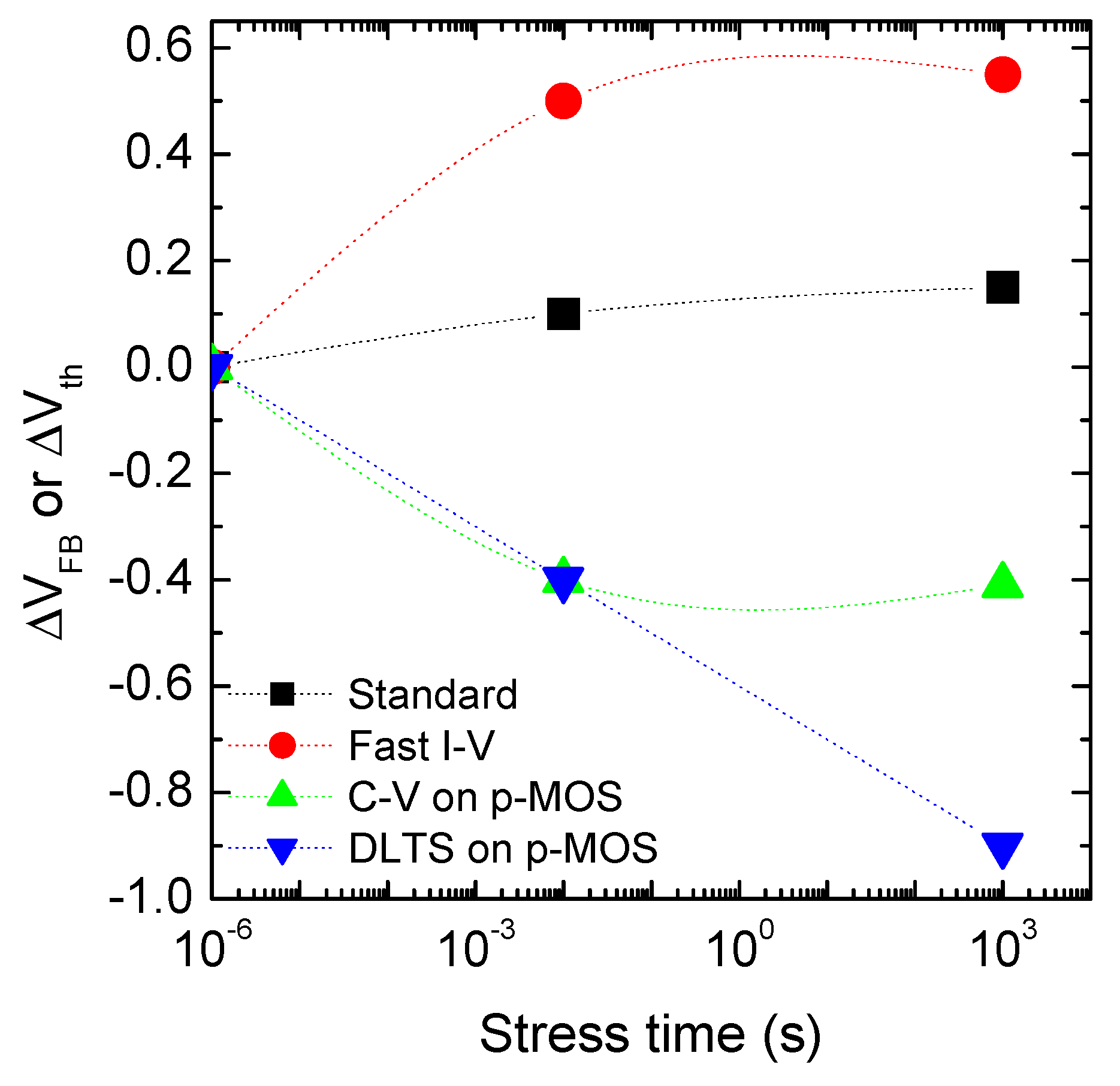
Figure 11 shows a comparison of different techniques to determine the shift ΔVth in MOSFETs (current measurements) and the flat band voltage shift ΔVFB in MOS capacitors (capacitance measurements). In Figure 11, the “standard” ΔVth measurement was obtained with a full IDS–VGS transcharacteristic, i.e., sweeping the gate bias from negative to large positive values (changing the polarization direction). In the fast I–V method, the MOSFET drain current ID was measured at VG = 6.5, 7.0, and 7.5 V, and the ΔVth values were estimated from the shift of the curves at constant IDS. In the C–V method, the C–V curves on p-type MOS capacitors were obtained in a range from −15 to −3 V. Then, ΔVFB values were estimated from the shift of the C–V curves at constant capacitance in the depletion region, taking 10 s to collect the information. Traps with a relaxation time shorter than the measurement time are not detectable. In the CC-DLTS method (constant capacitance deep level transient spectroscopy), the gate voltages of the constant capacitance were measured with a time resolution of 10 ms. In particular, after the gate bias stress, the properly designed measurement circuit allowed the monitoring of the gate bias needed to obtain the fixed capacitance value. Then, the gate voltage shift was regarded as ΔVFB. Thus, the DLTS method allows the detection of traps with a relaxation time four decades shorter than standard methods.
As can be noticed in Figure 11, the flat band voltage shift ΔVFB determined by standard C–V measurements (ΔVFB ~ – 0.4 V) by sweeping the VG in a wide range is comparable to that measured on MOSFETs (ID–VG). On the other hand, a deep-level transient spectroscopy (DLTS) method has been used to perform fast C–V measurements at constant gate capacitance. Hence, thanks to the reduction of the time needed to measure the Vth shift, it was possible to better estimate the amount of NIOTs. In fact, after the same stress time (i.e., 1000 s at VG = −15 V), the ΔVth estimated with fast C–V measurements is more than doubled compared with that measured with standard C–V measurements. This can be understood considering that the charge from the semiconductor substrate needs time to access the NIOTs via tunnelling. In particular, according to the Wentzel–Kramers–Brillouin approximation, a single tunnelling happens at a certain distance in logarithmic time. Bauza and Ghibaudo [72] have presented a single tunnelling model to describe the trapping phenomena in silicon MOS capacitors. However, interface traps contribute to the trapping phenomena due to the increased tunnelling probability. In 4H-SiC MOSFETs the Dit is two orders of magnitude larger than in silicon. Hence, Dit must be taken into account to study the NIOTs trapping phenome. According to Paulsen et al [73], the τ(x) tunnelling times needed to reach the NIOTs from the 4H-SiC substrate can be calculated as a function of the distance from the interface toward the bulk of the insulator, according to:
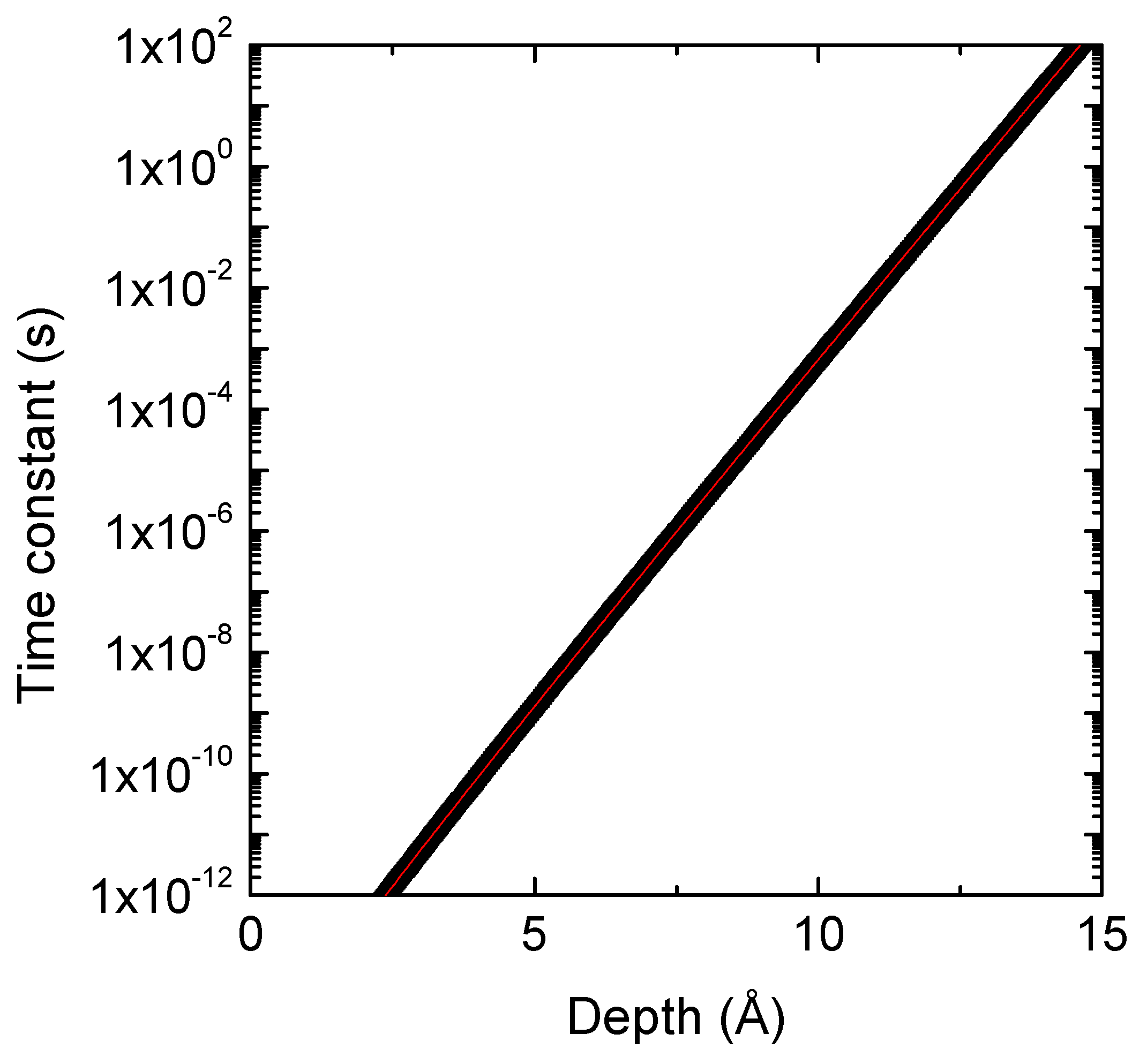
where η1 and η2 are functions of the doping of the material, and where m1* is the effective mass for electrons in the oxide [73]. Furthermore, ħ is the reduced Plank constant. Using the literature values of m1* [74], Equation (5) can be drawn as a function of the distance x between the NIOTs and the SiO2/4H-SiC interface. Thus, the tunnelling time constant as a function of the NIOTs distance and the SiO2/4H-SiC interface is shown in Figure 12.
Clearly, a long stress time is needed to charge NIOTs located far away from the SiO2/4H-SiC interface. In order to freeze the charged NIOTs, it is preferable to avoid the interruption of the gate bias and to reduce as much as possible the time needed to perform the Vth shift measurement. In the last decade, several time-resolved capacitance- and current-measurements have been employed to investigate the NIOTs [13,14,75]. A faster time resolution provides more information on NIOTs close to the SiO2/4H-SiC interface. Recently Pande et al [76] presented a method to investigate NIOTs on MOS capacitors in strong accumulation based on AC current measurements, with a time resolution of a few tenths of a nanosecond (~10−8 s). With this method, an amount of NIOTs in the order of 1013 cm−2 has been measured. Clearly, looking at Figure 12, with a time resolution of 10−8 s the NIOTs located within the first 5 Å from SiO2/4H-SiC interface results are unmeasurable.
4.2. Chemical Nature of the NIOTs
The chemical nature of the NIOTs has been theoretically debated [77,78]. In particular, C-C dimers and interstitial silicon atoms create both interface and near interface states at the SiO2/SiC interfaces. However, a clear identification and unification of the different processes is not yet provided. In order to gain deep insight into the chemical nature of the NIOTs responsible for the Vth instability, and on the near SiO2/4H-SiC interface region, several microscopic chemical investigations have been presented in literature in the last decade [52,53,79,80]. The different results reported in literature are often due to the variety of SiO2/SiC interface processing. In particular, first Zheleva et al. [79] and then Biggerstaff et al. [80] have investigated the SiO2/SiC interface at nanoscale, employing transmission electron microscopy (TEM). They detected the presence of a transition layer (up to several nanometers thick) containing carbon atoms at the SiO2/4H-SiC interface in thermally grown oxides onto 4H-SiC. However, the last generation of thermally grown oxides is much different than those pioneering works. In fact, Regoutz et al [53], using X-ray photoemission spectroscopy (XPS), have recently demonstrated the presence of an amount of N–C–Si bonds at the interface, which depends on the different nitridation processes. Clearly, the SiO2/SiC interfaces described in the literature are often difficult to compare, since different processes are used for the SiO2 deposition/growth or for the passivation of the interface states.
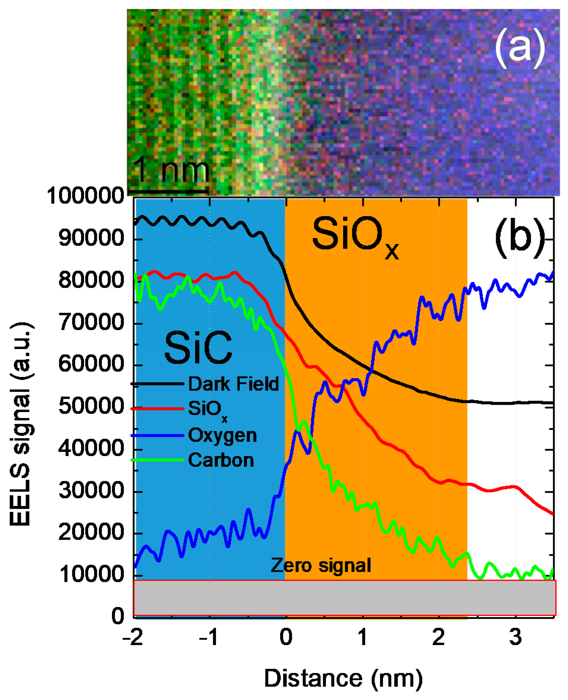
Recently, Fiorenza et al. [52] have reported on the presence of a narrow sub-stoichiometric SiOx layer produced on the re-oxidation of the 4H-SiC surface, even during nitridation (i.e., NO and N2O thermal treatments can move the SiO2/4H-SiC oxidation interface) of a deposited oxide layer. In particular, sub-Ångström resolution scanning transmission electron microscopy (STEM) analyses combined with electron energy loss spectroscopy (EELS) have been used to monitor the chemical environment of the first nanometer of insulator from the 4H-SiC interface. Furthermore, the nano-chemical investigation was correlated with the time-dependent capacitance measurements and correlated with the NIOTs responsible for the MOSFET threshold voltage instability [52].
Figure 13a shows the cross-section of the SiO2/4H-SiC interface in high resolution dark field (DF) spectrum image that simultaneously collected all the elemental EELS maps. The chemical element profiling a sub-stoichiometric SiOx layer was obtained from the Silicon map using a 4 eV wide energy window between 99 and 103 eV (Figure 13b). In fact, in this 4 eV wide energy window, only the silicon atoms not completely oxidized (surrounded by four oxygen atoms) can give a contribution to the EELS spectrum above the noise limit. Figure 13b highlights the progressive change in the SiOx and oxygen profiles across the SiO2/4H-SiC interface. This experimental evidence suggests the presence of a non-abrupt (NA) SiO2/4H-SiC interface. Furthermore, the carbon profile decreases within the oxide, with a tail that is wider than one nanometre.
In this scenario, clearly further investigations are needed to correlate the Vth instability with particular NIOTs and to identify their chemical nature. Then, an appropriate technological strategy to overcome this issue has to be pursued to further improve the performances and the reliability concerns of commercial 4H-SiC power MOSFETs.
5. Conclusions
This review paper presented some relevant characterization aspects of the SiO2/SiC system in 4H-SiC MOSFETs. A special emphasis is given to the need to correlate several standard and nanoscale electro-structural techniques, in order to have an exhaustive scenario of the SiO2/4H-SiC properties and a better comprehension of the 4H-SiC MOSFET physics in relation to the device’s processing steps. In particular, it has been shown that NIOTs have a strong influence on the device’s electrical behaviour. The cross correlation of time dependent electrical measurements with structural analyses enabled the estimatation of a typical amount of NIOTs of 1011 cm−2 inside the SiO2 (within 1–2 nm from the SiC interface) and attribute them to the presence of a sub-stoichiometric SiOx layer at the interface. Hence, to characterize these interfaces, advanced time resolved fast electrical measurements are mandatory to discriminate between different traps at the interface and within the oxide.
Author Contributions
Conceptualization, Writing-Original Draft Preparation, P.F.; Writing-Review & Editing, Supervision, Project Administration, F.R.; Methodology, Investigation, F.G.
Funding
This work was partially carried out in the framework of European project WInSiC4AP (Wide Band Gap Innovative SiC for Advanced Power), funded by the ECSEL JU under grant agreement No.737483. This Joint Undertaking receives support from the European Union’s Horizon 2020 research and innovation programme and Czech Republic, France, Germany, Italy. The WInSiC4AP project is also supported by ESI funds from MIUR 2014-2020 FESR program.
Acknowledgments
The authors would like to acknowledge M. Saggio and F. Iucolano (STMicroelectronics) and their teams for the collaboration. In particular, A. Parisi and S. Reina are acknowledged for support during electrical characterization. Moreover, the authors thank all their colleagues of CNR-IMM. In particular, A. La Magna and I. Deretzis for support with theoretical calculations, G. Nicotra and C. Bongiono for TEM investigation, S. Di Franco for devices processing, R. Lo Nigro, G. Greco and E. Schilirò for fruitful discussions.
Conflicts of Interest
The authors declare no conflict of interest.
References
- Cooper, J.A.; Islam, N.; Ramamurthy, R.P.; Sampath, M.; Morisette, D.T. Vertical Tri-Gate Power MOSFETs in 4H-SiC. Mater. Sci. Forum 2018, 924, 680–683. [Google Scholar] [CrossRef]
- Ohashi, H. Power devices then and now, strategy of Japan. In Proceedings of the 24th International Symposium on Power Semiconductor Devices and ICs (ISPSD2012), Bruges, Belgium, 3–7 June 2012; pp. 9–12. [Google Scholar] [CrossRef]
- Baliga, B.J. Silicon Carbide Power Devices; World Scientific Co. Pte. Ltd.: Singapore, Singapore, 2005. [Google Scholar]
- Schilirò, E.; Lo Nigro, R.; Fiorenza, P.; Roccaforte, F. Negative charge trapping effects in Al2O3 films grown by atomic layer depositiononto thermally oxidized 4H-SiC. AIP Adv. 2016, 6, 075021. [Google Scholar] [CrossRef]
- Hosoi, T.; Azumo, S.; Kashiwagi, Y.; Hosaka, S.; Nakamura, R.; Mitani, S.; Nakano, Y.; Asahara, H.; Nakamura, T.; Kimoto, T.; et al. Performance and Reliability Improvement in SiC Power MOSFETs by Implementing AlON High-k Gate Dielectrics. In Proceedings of the 2012 International Electron Devices Meeting, San Francisco, CA, USA, 10–13 December 2012. [Google Scholar] [CrossRef]
- Kimoto, T. Material science and device physics in SiC technology for high-voltage power devices. Jpn. J. Appl. Phys. 2015, 54, 040103. [Google Scholar] [CrossRef]
- Cabello, M.; Soler, V.; Rius, G.; Montserrat, J.; Rebollo, J.; Godignon, P. Advanced processing for mobility improvement in 4H-SiC MOSFETs: A review. Mater. Sci. Semicon. Proc. 2018, 78, 22–31. [Google Scholar] [CrossRef]
- Roccaforte, F.; Fiorenza, P.; Greco, G.; Lo Nigro, R.; Giannazzo, F.; Iucolano, F.; Saggio, M. Emerging trends in wide band gap semiconductors (SiC and GaN) technology for power devices. Microelectron. Eng. 2018, 187–188, 66–77. [Google Scholar] [CrossRef]
- Yano, H.; Kanafuji, N.; Osawa, A.; Hatayama, T.; Fuyuki, T. Threshold Voltage Instability in 4H-SiC MOSFETs With Phosphorus-Doped and Nitrided Gate Oxides. IEEE Trans. Electron. Devices 2015, 62, 324–332. [Google Scholar] [CrossRef]
- Lelis, A.J.; Green, R.; Habersat, D.B.; El, M. Basic Mechanisms of Threshold-Voltage Instability and Implications for Reliability Testing of SiC MOSFETs. IEEE Trans. Electron Devices 2015, 62, 316–323. [Google Scholar] [CrossRef]
- Afanas’ev, V.V.; Stesmans, A. Interfacial Defects in SiO2 Revealed by Photon Stimulated Tunneling of Electrons. Phys. Rev. Lett. 1997, 78, 2437. [Google Scholar] [CrossRef]
- Pensl, G.; Ciobanu, F.; Frank, T.; Kirmse, D.; Krieger, M.; Reshanov, S.; Schmid, F.; Weidner, M.; Ohshima, T.; Itoh, H.; et al. Defect-engineering in SiC by ion implantation and electron irradiation. Microelectron. Eng. 2006, 83, 146–149. [Google Scholar] [CrossRef]
- Zhang, X.; Okamoto, D.; Hatakeyama, T.; Sometani, M.; Harada, S.; Kosugi, R.; Iwamuro, N.; Yano, H. Characterization of near-interface traps at 4H-SiC metal–oxide–semiconductor interfaces using modified distributed circuit model. Appl. Phys. Express 2017, 10, 064101. [Google Scholar] [CrossRef]
- Fujino, Y.; Kita, K. Quantitative Characterization of Near-Interface Oxide Traps in 4H-SiC MOS Capacitors by Transient Capacitance Measurements. ECS Trans. 2015, 69, 219–225. [Google Scholar] [CrossRef]
- Umeda, T.; Esaki, K.; Kosugi, R.; Fukuda, K.; Ohshima, T.; Morishita, N.; Isoya, J. Behavior of nitrogen atoms in SiC-SiO2 interfaces studied by electrically detected magnetic resonance. Appl. Phys. Lett. 2011, 99, 142105. [Google Scholar] [CrossRef]
- Roccaforte, F.; Fiorenza, P.; Greco, G.; Lo Nigro, R.; Giannazzo, F.; Patti, A.; Saggio, M. Challenges for energy efficient wide band gap semiconductor power devices. Phys. Status Solidi A 2014, 211, 2063–2071. [Google Scholar] [CrossRef]
- Li, H.-F.; Dimitrijev, S.; Harrison, H.B.; Sweatman, D. Interfacial characteristics of N2O and NO nitrided SiO2 grown on SiC by rapid thermal processing. Appl. Phys. Lett. 1997, 70, 2028. [Google Scholar] [CrossRef]
- Chung, G.Y.; Tin, C.C.; Williams, J.R.; McDonald, K.; Di Ventra, M.; Pantelides, S.T.; Feldman, L.C.; Weller, R.A. Effect of nitric oxide annealing on the interface trap densities near the band edges in the 4H polytype of silicon carbide. Appl. Phys. Lett. 2000, 76, 1713. [Google Scholar] [CrossRef]
- Lipkin, L.A.; Das, M.K.; Palmour, J.W. N2O Processing Improves the 4H-SiC:SiO2 Interface. Mater. Sci. Forum 2002, 389–393, 985–988. [Google Scholar] [CrossRef]
- Lu, C.-Y.; Cooper, J.A.; Tsuji, T.; Chung, G.; Williams, J.R.; McDonald, K.; Feldman, L.C. Effect of process variations and ambient temperature on electron mobility at the SiO2/4H-SiC interface. IEEE Trans. Electron Devices 2003, 50, 1582–1588. [Google Scholar]
- Harada, S.; Kosugi, R.; Senzaki, J.; Cho, W.-J.; Fukuda, K.; Arai, K. Relationship between channel mobility and interface state density in SiC metal–oxide–semiconductor field-effect transistor. J. Appl. Phys. 2002, 91, 1568. [Google Scholar] [CrossRef]
- Pérez-Tomás, A.; Brosselard, P.; Godignon, P.; Millán, J.; Mestres, N.; Jennings, M.R.; Covington, J.A.; Mawby, P.A. Field-effect mobility temperature modeling of 4H-SiC metal-oxide-semiconductor transistors. J. Appl. Phys. 2006, 100, 114508. [Google Scholar] [CrossRef]
- Jamet, P.; Dimitrijev, S.; Tanner, P. Effects of nitridation in gate oxides grown on 4H-SiC. J. Appl. Phys. 2001, 90, 5058. [Google Scholar] [CrossRef]
- Dhar, S.; Ahyi, A.C.; Williams, J.R.; Ryu, S.-H.; Agarwal, A.K. Temperature Dependence of Inversion Layer Carrier Concentration and Hall Mobility in 4H-SiC MOSFETs. Mater. Sci. Forum 2012, 717–720, 713. [Google Scholar] [CrossRef]
- Chung, G.Y.; Tin, C.C.; Williams, J.R.; McDonald, K.; Chanana, R.K.; Weller, R.A.; Pantelides, S.T.; Feldman, L.C.; Holland, O.W.; Das, M.K.; et al. Improved Inversion Channel Mobility for 4H-SiC MOSFETs Following High Temperature Anneals in Nitric Oxide. IEEE Electron Devices Lett. 2001, 22, 176–178. [Google Scholar] [CrossRef]
- Kosugi, R.; Fukuda, K.; Arai, K. High Temperature Rapid Thermal Oxidation and Nitridation of 4H-SiC in Diluted N2O and NO Ambient. Mater. Sci. Forum 2005, 483–485, 669–672. [Google Scholar] [CrossRef]
- Wang, Y.; Tang, K.; Khan, T.; Balasubramanian, M.K.; Naik, H.; Wang, W.; Chow, T.P. The effect of gate oxide processes on the performance of 4H-SiC MOSFETs and gate-controlled diodes. IEEE Trans. Electron Devices 2008, 55, 2046–2053. [Google Scholar] [CrossRef]
- Rozen, J.; Ahyi, A.C.; Zhu, X.; Williams, J.R.; Feldman, L.C. Scaling Between Channel Mobility and Interface State Density in SiC MOSFETs. IEEE Trans. Electron Devices 2011, 58, 3808–3811. [Google Scholar] [CrossRef]
- Frazzetto, A.; Giannazzo, F.; Fiorenza, P.; Raineri, V.; Roccaforte, F. Limiting mechanism of inversion channel mobility in Al-implanted lateral 4H-SiC metal-oxide semiconductor field-effect transistors. Appl. Phys. Lett. 2011, 99, 072117. [Google Scholar] [CrossRef]
- Fiorenza, P.; Giannazzo, F.; Frazzetto, A.; Roccaforte, F. Influence of the surface morphology on the channel mobility of lateral implanted 4H-SiC(0001) metal-oxide-semiconductor field-effect transistors. J. Appl. Phys. 2012, 112, 084501. [Google Scholar] [CrossRef] [Green Version]
- Dhar, S.; Wang, S.; Williams, J.; Pantelides, S.; Feldman, L. Interface Passivation for Silicon Dioxide Layers on Silicon Carbide. MRS Bull. 2005, 30, 288–292. [Google Scholar] [CrossRef]
- Kobayashi, T.; Suda, J.; Kimoto, T. Reduction of interface state density in SiC (0001) MOS structures by post-oxidation Ar annealing at high temperature. AIP Adv. 2017, 7, 045008. [Google Scholar] [CrossRef] [Green Version]
- Hatakeyama, T.; Kiuchi, Y.; Sometani, M.; Harada, S.; Okamoto, D.; Yano, H.; Yonezawa, Y.; Okumura, H. Characterization of traps at nitrided SiO2/SiC interfaces near the conduction band edge by using Hall effect measurements. Appl. Phys. Express 2017, 10, 046601. [Google Scholar] [CrossRef]
- Asaba, S.; Schimizu, T.; Nakabayashi, Y.; Fukatsu, S.; Ito, T.; Iijima, R. Novel Gate Insulator Process by Nitrogen Annealing for Si-Face SiC MOSFET with High-Mobility and High-Reliability. Mater. Sci. Forum 2018, 924, 457. [Google Scholar] [CrossRef]
- Schroder, D.K. Semiconductor Material and Device Characterization, 3rd ed.; Wiley: Hoboken, NJ, USA, 2006. [Google Scholar]
- Martens, K.; On Chui, C.; Brammertz, G.; De Jaeger, B.; Kuzum, D.; Meuris, M.; Heyns, M.M.; Krishnamohan, T.; Saraswat, K.; Maes, H.E.; et al. On the Correct Extraction of Interface Trap Density of MOS Devices with High-Mobility Semiconductor Substrates. IEEE Trans. Electron Devices 2008, 55, 547. [Google Scholar] [CrossRef]
- Yoshioka, H.; Nakamura, T.; Kimoto, T. Generation of very fast states by nitridation of the SiO2/SiC interface. J. Appl. Phys. 2012, 111, 014502. [Google Scholar] [CrossRef]
- Nakazawa, S.; Okuda, T.; Suda, J.; Nakamura, T.; Kimoto, T. Interface Properties of 4H-SiC (11¯20) and (1¯100) MOS Structures Annealed in NO. IEEE Trans. Electron Devices 2015, 62, 309. [Google Scholar] [CrossRef]
- Groeseneken, G.; Maes, H.E.; Beltran, N.; DeKeersmaecker, R.F. A reliable approach to charge-pumping measurements in MOS transistors. IEEE Trans. Electron Devices 1984, ED-31, 42–53. [Google Scholar] [CrossRef]
- Okamoto, D.; Yano, H.; Hatayama, T.; Uraoka, Y.; Fuyuki, T. Analysis of Anomalous Charge-Pumping Characteristics on 4H-SiC MOSFETs. IEEE Trans. Electron Devices 2008, 55, 2013. [Google Scholar] [CrossRef]
- Salinaro, A.; Pobegen, G.; Aichinger, T.; Zippelius, B.; Peters, D.; Friedrichs, P.; Frey, L. Charge Pumping Measurements on Differently Passivated Lateral 4H-SiC MOSFETs. IEEE Trans. Electron Devices 2015, 62, 155. [Google Scholar] [CrossRef]
- Saks, N.S.; Agarwal, A.K. Hall mobility and free electron density at the SiC/SiO2 interface in 4H-SiC. Appl. Phys. Lett. 2000, 77, 3281–3283. [Google Scholar] [CrossRef]
- Uhnevionak, V.; Burenkov, A.; Strenger, C.; Ortiz, G.; Bedel-Pereira, E.; Mortet, V.; Cristiano, F.; Bauer, A.J.; Pichler, P. Comprehensive Study of the Electron Scattering Mechanisms in 4H-SiC MOSFETs. IEEE Trans. Electron Devices 2015, 62, 2562–2570. [Google Scholar] [CrossRef]
- Hauck, M.; Lehmeyer, J.; Pobegen, G.; Weber, H.B.; Krieger, M. An adapted method for analyzing 4H silicon carbide metal-oxide-semiconductor field-effect transistors. Commun. Phys. 2019, 2, 5. [Google Scholar]
- Cabello, M.; Soler, V.; Haasmann, D.; Montserrat, J.; Rebollo, J.; Godignon, P. Evidence of Channel Mobility Anisotropy on 4H-SiC MOSFETs with Low Interface Trap Density Invited Poster ECSCRM 2018. Available online: https://warwick.ac.uk/fac/sci/eng/ecscrm2018/programme/ecscrm_programme_2018.pdf (accessed on 20 May 2019).
- Fiorenza, P.; Di Franco, S.; Giannazzo, F.; Roccaforte, F. Nanoscale probing of the lateral homogeneity of donors concentration in nitridated SiO2/4H-SiC interfaces. Nanotechnology 2016, 27, 315701. [Google Scholar] [CrossRef] [PubMed]
- Fiorenza, P.; Giannazzo, F.; Swanson, L.K.; Frazzetto, A.; Lorenti, S.; Alessandrino, M.S.; Roccaforte, R. A look underneath the SiO2/4H-SiC interface after N2O thermal treatments. Beilstein J. Nanotechnol. 2013, 4, 249–254. [Google Scholar] [CrossRef] [PubMed]
- Saitoh, H.; Seki, A.; Manabe, A.; Kimoto, T. Interface Properties of SiO2/4H-SiC(0001) with Large Off-Angles Formed by N2O Oxidation. Mater. Sci. Forum 2007, 556–557, 659–662. [Google Scholar] [CrossRef]
- Kosugi, R.; Umeda, T.; Sakuma, Y. Fixed nitrogen atoms in the SiO2/SiC interface region and their direct relationship to interface trap density. Appl. Phys. Lett. 2011, 99, 182111. [Google Scholar] [CrossRef]
- Swanson, L.K.; Fiorenza, P.; Giannazzo, F.; Frazzetto, A.; Roccaforte, F. Correlating macroscopic and nanoscale electrical modifications of SiO2/4H-SiC interfaces upon post-oxidation-annealing in N2O and POCl3. Appl. Phys. Lett. 2012, 101, 193501. [Google Scholar] [CrossRef]
- Fiorenza, P.; Giannazzo, F.; Vivona, M.; La Magna, A.; Roccaforte, F. SiO2/4H-SiC interface doping during post-deposition-annealing of the oxide in N2O or POCl3. Appl. Phys. Lett. 2013, 103, 153508. [Google Scholar] [CrossRef]
- Fiorenza, P.; Iucolano, F.; Nicotra, G.; Bongiorno, C.; Deretzis, I.; La Magna, A.; Giannazzo, F.; Saggio, M.; Spinella, C.; Roccaforte, F. Electron trapping at SiO2/4H-SiC interface probed by transient capacitance measurements and atomic resolution chemical analysis. Nanotechnology 2018, 29, 395702. [Google Scholar] [CrossRef] [PubMed]
- Regoutz, A.; Pobegen, G.; Aichinger, T. Interface chemistry and electrical characteristics of 4H-SiC/SiO2 after nitridation in varying atmospheres. J. Mater. Chem. C 2018, 6, 12079. [Google Scholar] [CrossRef]
- Giannazzo, F.; Fiorenza, P.; Raineri, V. Carrier transport in advanced semiconductor materials. In Applied Scanning Probe Methods X; Springer: Berlin/Heidelberg, Germany, 2008; pp. 63–103. [Google Scholar]
- Fiorenza, P.; Vivona, M.; Iucolano, F.; Severino, A.; Lorenti, S.; Nicotra, G.; Bongiorno, C.; Giannazzo, F.; Roccaforte, F. Temperature-dependent Fowler-Nordheim electron barrier height in SiO2/4H-SiC MOS capacitors. Mater. Sci. Semicon. Process. 2018, 78, 38–42. [Google Scholar] [CrossRef]
- Okamoto, D.; Yano, H.; Hirata, K.; Hatayama, T.; Fuyuki, T. Improved Inversion Channel Mobility in 4H-SiC MOSFETs on Si Face Utilizing Phosphorus-Doped Gate Oxide. IEEE Electron Devices Lett. 2010, 31, 710–712. [Google Scholar] [CrossRef]
- Yano, H.; Araoka, T.; Hatayama, T.; Fuyuki, T. Improved Stability of 4H-SiC MOS Device Properties by Combination of NO and POCl3 Annealing. Mater. Sci. Forum 2013, 740–742, 727–732. [Google Scholar] [CrossRef]
- Sharma, Y.K.; Ahyi, A.C.; Isaacs-Smith, T.; Modic, A.; Park, M.; Xu, Y.; Garfunkel, E.L.; Dhar, S.; Feldman, L.C.; Williams, J.R. High-Mobility Stable 4H-SiC MOSFETs Using a Thin PSG Interfacial Passivation Layer. IEEE Electron Devices Lett. 2013, 34, 175–177. [Google Scholar] [CrossRef]
- Modic, A.; Liu, G.; Ahyi, A.C.; Zhou, Y.; Xu, P.; Hamilton, M.C.; Williams, J.R.; Feldman, L.C.; Dhar, S. High Channel Mobility 4H-SiC MOSFETs by Antimony Counter-Doping. IEEE Electron Devices Lett. 2014, 35, 894. [Google Scholar] [CrossRef]
- Lichtenwalner, D.J.; Cheng, L.; Dhar, S.; Agarwal, A.; Palmour, J.W. High mobility 4H-SiC (0001) transistors using alkali and alkaline earth interface layers. Appl. Phys. Lett. 2014, 105, 182107. [Google Scholar] [CrossRef]
- Okamoto, D.; Sometani, M.; Harada, S.; Kosugi, R.; Yonezawa, Y.; Yano, H. Improved Channel Mobility in 4H-SiC MOSFETs by Boron Passivation. IEEE Electron Devices Lett. 2014, 35, 1176–1178. [Google Scholar] [CrossRef]
- Huston Dycus, J.; Xu, W.; Lichtenwalner, D.J.; Hull, B.; Palmour, J.W.; LeBeau, J.M. Structure and chemistry of passivated SiC/SiO2 interfaces. Appl. Phys. Lett. 2016, 108, 201607. [Google Scholar] [CrossRef]
- Yang, X.; Lee, B.; Misra, V. High Mobility 4H-SiC Lateral MOSFETs Using Lanthanum Silicate and Atomic Layer Deposited SiO2. IEEE Electron Devices Lett. 2015, 36, 312–314. [Google Scholar] [CrossRef]
- Li, X.; Ermakov, A.; Amarasinghe, V.; Garfunkel, E.; Gustafsson, T.; Feldman, L.C. Oxidation induced stress in SiO2/SiC structures. Appl. Phys. Lett. 2017, 110, 141604. [Google Scholar] [CrossRef]
- Lichtenwalner, D.J.; Cheng, L.; Dhar, S.; Agarwal, A.K.; Allen, S.; Palmour, J.W. High-Mobility SiC MOSFETs with Chemically Modified Interfaces. Mater. Sci. Forum 2015, 821–823, 749. [Google Scholar] [CrossRef]
- Fiorenza, P.; Swanson, L.K.; Vivona, M.; Giannazzo, F.; Bongiorno, C.; Frazzetto, A.; Roccaforte, F. Comparative study of gate oxide in 4H-SiC lateral MOSFETs subjected to post-deposition-annealing in N2O and POCl3. Appl. Phys. A 2014, 115, 333. [Google Scholar] [CrossRef]
- Aviñó Salvadó, O.; Morel, H.; Buttay, C.; Labrousse, D.; Lefebvre, S. Threshold voltage instability in SiC MOSFETs as a consequence of current conduction in their body diode. Microelectron. Reliab. 2018, 88–90, 636. [Google Scholar]
- Fiorenza, P.; Greco, G.; Giannazzo, F.; Iucolano, F.; Roccaforte, F. Effects of interface states and near interface traps on the threshold voltage stability of GaN and SiC transistors employing SiO2 as gate dielectric. J. Vacuum Sci. Technol. B 2017, 35, 01A101. [Google Scholar] [CrossRef]
- Fiorenza, P.; Frazzetto, A.; Guarnera, A.; Saggio, M.; Roccaforte, F. Fowler-Nordheim tunneling at SiO2/4H-SiC interfaces in metal-oxide-semiconductor field effect transistors. Appl. Phys. Lett. 2014, 105, 142108. [Google Scholar] [CrossRef]
- Fiorenza, P.; La Magna, A.; Vivona, M.; Roccaforte, F. Near interface traps in SiO2/4H-SiC metal-oxide-semiconductor field effect transistors monitored by temperature dependent gate current transient measurements. Appl. Phys. Lett. 2016, 109, 012102. [Google Scholar] [CrossRef]
- Hayashi, M.; Sometani, M.; Hatakeyama, T.; Yano, H.; Harada, S. Hole trapping in SiC-MOS devices evaluated by fast-capacitance–voltage method. Jpn. J. Appl. Phys. 2018, 57, 04FR15. [Google Scholar] [CrossRef]
- Bauza, D.; Ghibaudo, G. Analytical study of the contribution of fast and slow oxide traps to the charge pumping current in MOS structures. Solid-State Electron. 1996, 39, 563–570. [Google Scholar] [CrossRef]
- Paulsen, R.E.; Siergiej, R.R.; French, M.L.; White, M.H. Observation of Near-Interface Oxide Traps with the Charge-Pumping Technique. IEEE Electron Device Lett. 1992, 13, 627–629. [Google Scholar] [CrossRef]
- Chanana, R.K.; McDonald, K.; Di Ventra, M.; Pantelides, S.T.; Feldman, L.C.; Chung, G.Y.; Tin, C.C.; Williams, J.R.; Weller, R.A. Fowler–Nordheim hole tunneling in p-SiC/SiO2 structures. Appl. Phys. Lett. 2000, 77, 2560. [Google Scholar] [CrossRef]
- Aichinger, T.; Rescher, G.; Pobegen, G. Threshold voltage peculiarities and bias temperature instabilities of SiC MOSFETs. Microelectron. Reliab. 2018, 80, 68–78. [Google Scholar] [CrossRef]
- Pande, P.; Dimitrijev, S.; Haasmann, D.; Amini Moghadam, H.; Tanner, P.; Han, J. Direct Measurement of Active Near-Interface Traps in the Strong-Accumulation Region of 4H-SiC MOS Capacitors. IEEE J. Electron Devices Soc. 2018, 6, 468. [Google Scholar] [CrossRef]
- Knaup, J.M.; Deák, P.; Frauenheim, T.; Gali, A.; Hajnal, Z.; Choyke, W.J. Defects in SiO2 as the possible origin of near interface traps in the SiC/SiO2 system: A systematic theoretical study. Phys. Rev. B 2005 72, 115323.
- Devynck, F.; Alkauskas, A.; Broqvist, P.; Pasquarello, A. Charge transition levels of carbon-, oxygen-, and hydrogen-related defects at the SiC/SiO2 interface through hybrid functionals. Phys. Rev. B 2011, 84, 235320. [Google Scholar] [CrossRef]
- Zheleva, T.; Lelis, A.; Duscher, G.; Liu, F.; Levin, I.; Das, M. Transition layers at the SiO2/Si C interface. Appl. Phys. Lett. 2008, 93, 022108. [Google Scholar] [CrossRef]
- Biggerstaff, T.L.; Reynolds, C.L., Jr.; Zheleva, T.; Lelis, A.; Habersat, D.; Haney, S.; Ryu, S.-H.; Agarwal, A.; Duscher, G. Relationship between 4H-SiC/SiO2 transition layer thickness and mobility. Appl. Phys. Lett. 2009, 95, 032108. [Google Scholar] [CrossRef]
Figure 1.
Comparison of Ron,sp as a function of the breakdown voltage breakdown voltage (BV) for Si and 4H-SiC power metal oxide semiconductor field effect transistors (MOSFETs). The solid lines are the theoretical unipolar limit. The experimental data are taken from Reference [2].
Figure 1.
Comparison of Ron,sp as a function of the breakdown voltage breakdown voltage (BV) for Si and 4H-SiC power metal oxide semiconductor field effect transistors (MOSFETs). The solid lines are the theoretical unipolar limit. The experimental data are taken from Reference [2].

Figure 2.
Cross section of a planar 4H-SiC power MOSFET. The vertical path of the current from source to drain electrode, as well as the resistive contributions, are also indicated.
Figure 2.
Cross section of a planar 4H-SiC power MOSFET. The vertical path of the current from source to drain electrode, as well as the resistive contributions, are also indicated.
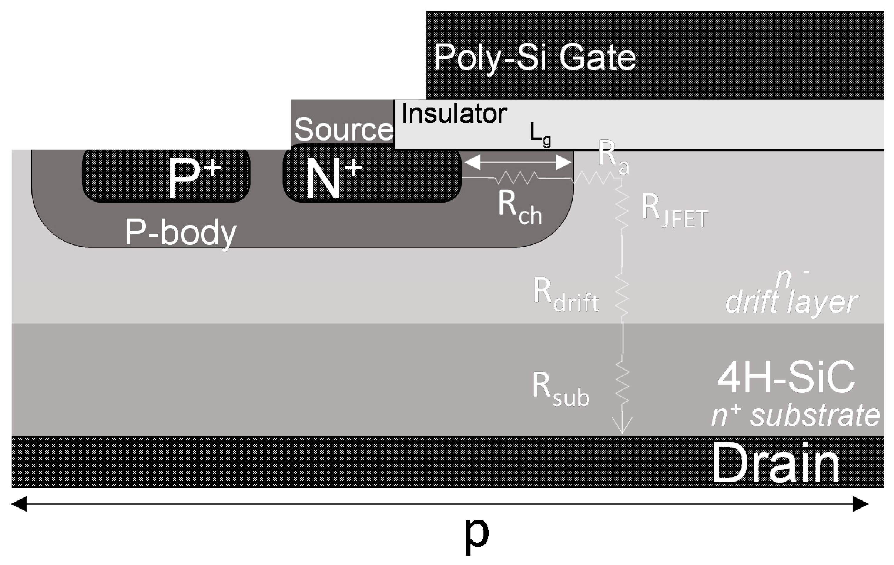
Figure 3.
Graphical representation of the SiO2/4H-SiC interface, indicating the regions of interest and interface states and oxide traps.
Figure 3.
Graphical representation of the SiO2/4H-SiC interface, indicating the regions of interest and interface states and oxide traps.
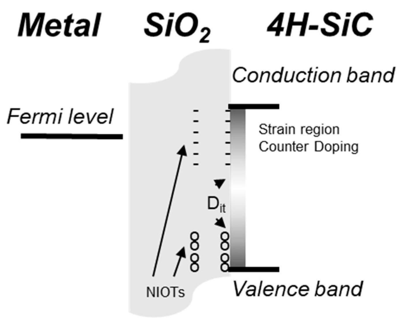
Figure 4.
Experimental field effect mobility µFE values as a function of the integral of the interface state density (Nit) evaluated with different methods. A clear correlation is obtained when Nit is evaluated using the C-ψ method. The data were taken from Reference [38].
Figure 4.
Experimental field effect mobility µFE values as a function of the integral of the interface state density (Nit) evaluated with different methods. A clear correlation is obtained when Nit is evaluated using the C-ψ method. The data were taken from Reference [38].

Figure 5.
Dispersion of the flat band voltage shift ΔVFB obtained from C–V measurements on 25 macroscopic MOS capacitors on a 6” wafer (a), and by scanning capacitance microscopy (SCM) measurements on arrays of 25 tip positions (with 1 μm spacing) (b).
Figure 5.
Dispersion of the flat band voltage shift ΔVFB obtained from C–V measurements on 25 macroscopic MOS capacitors on a 6” wafer (a), and by scanning capacitance microscopy (SCM) measurements on arrays of 25 tip positions (with 1 μm spacing) (b).

Figure 6.
(a) Surface morphology acquired with an AFM scan on the bare SiO2 surface, and (b) SCM map indicating a non-uniform spatial distribution of the surface potential.
Figure 6.
(a) Surface morphology acquired with an AFM scan on the bare SiO2 surface, and (b) SCM map indicating a non-uniform spatial distribution of the surface potential.
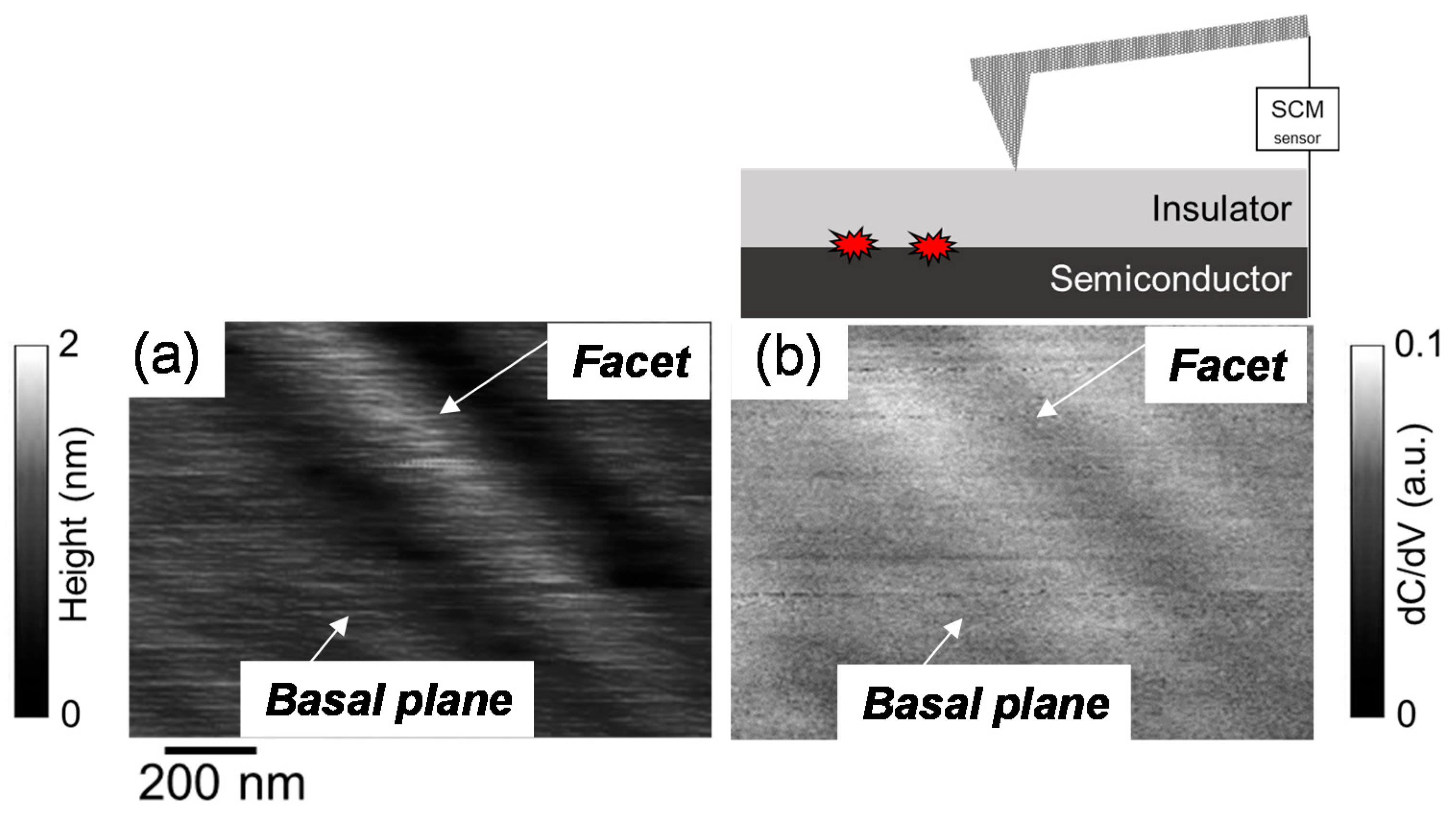
Figure 7.
SSRM (scanning spreading resistance microscopy) carrier concentration across the SiO2/4H-SiC interfaces on the as deposited (black line) and N2O annealed (blue line) samples.
Figure 7.
SSRM (scanning spreading resistance microscopy) carrier concentration across the SiO2/4H-SiC interfaces on the as deposited (black line) and N2O annealed (blue line) samples.

Figure 8.
Schematic of a stressed (a) and a relaxed (b) SiO2/4H-SiC interface. The thermal growth produces a compressive stress at the SiO2/4H-SiC interface that limit the MOSFET channel mobility. When the interfacial stress is released (e., the MOSFET channel mobility increases.
Figure 8.
Schematic of a stressed (a) and a relaxed (b) SiO2/4H-SiC interface. The thermal growth produces a compressive stress at the SiO2/4H-SiC interface that limit the MOSFET channel mobility. When the interfacial stress is released (e., the MOSFET channel mobility increases.
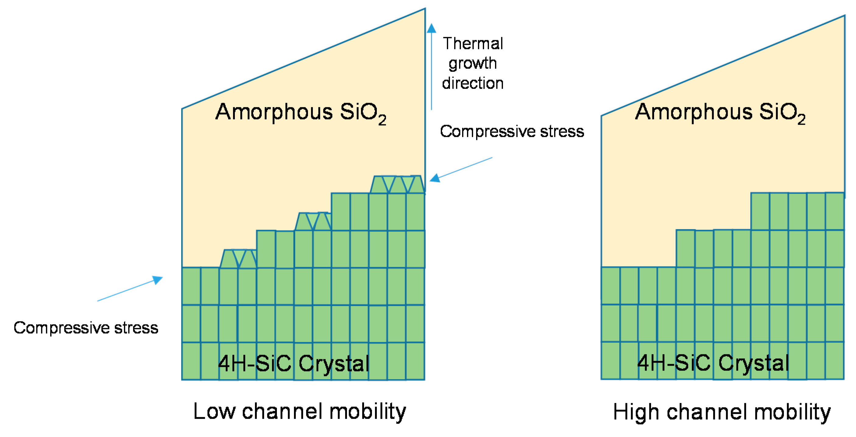
Figure 9.
Vth shift as a function of the gate bias stress time at 175 °C for two different device families: Gen1 and Gen2 commercial 4H-SiC MOSFETs. The data are taken from Reference [10].
Figure 9.
Vth shift as a function of the gate bias stress time at 175 °C for two different device families: Gen1 and Gen2 commercial 4H-SiC MOSFETs. The data are taken from Reference [10].

Figure 10.
(a) Threshold voltage (Vth) variation measured in a lateral 4H-SiC MOSFET after a gate stress bias loop. The arrow indicates the direction of the applied stress bias loop. (b) Inversion-to-accumulation and backward 1 kHz C–Vs of MOSFETs in gate-controlled diode configuration. The figure is adapted from References [52,68].

Figure 11.
ΔVFB (equivalent to ΔVth) as a function of the stress time measured with different electrical characterization techniques. Data taken from Reference [71].
Figure 11.
ΔVFB (equivalent to ΔVth) as a function of the stress time measured with different electrical characterization techniques. Data taken from Reference [71].

Figure 12.
Tunneling time constant obtained varying the depth between the near interface oxide traps (NIOTs) and the SiO2/4H-SiC interface. Data calculated from References [52,73] using Equation (5).

Figure 13.
(a) High-resolution spectrum imaging cross section STEM image of the SiO2/4H-SiC interface. (b) EELS spectra of carbon, oxygen, and partially oxidized silicon (SiOx). More details on these analyses are reported in Reference [52].
Figure 13.
(a) High-resolution spectrum imaging cross section STEM image of the SiO2/4H-SiC interface. (b) EELS spectra of carbon, oxygen, and partially oxidized silicon (SiOx). More details on these analyses are reported in Reference [52].

Table 1.
Summary of field effect mobility μFE and interface states density Dit data in 4H-SiC MOSFETs and MOS capacitors. The processing conditions of the gate oxide (on epitaxial or implanted body), the extraction method of Dit, and the doping NA of the p-type body concentration are also reported.
Table 1.
Summary of field effect mobility μFE and interface states density Dit data in 4H-SiC MOSFETs and MOS capacitors. The processing conditions of the gate oxide (on epitaxial or implanted body), the extraction method of Dit, and the doping NA of the p-type body concentration are also reported.
| Process | Temperature (°C) | µ (cm2V−1s−1) | Dit (cm−2eV−1) | Methods | NA (cm−3) | Ref. |
|---|---|---|---|---|---|---|
| Dry | 1175 | 4 | 9 × 10¹² | Gp/ω | 1 × 10¹⁶ epi | [19,21] |
| NO | 1175 | 32 | N.A. | N.A. | 8 × 10¹⁵ epi | [20,25] |
| NO 10 min | 1250 | 20 | 2 × 10¹⁴ | Hall | 1.3 × 10¹⁵ | [33] |
| NO 60 min | 1250 | 38 | 8 × 10¹³ | Hall | 2.3 × 10¹⁵ | [28,33] |
| NO 120 min | 1250 | 34 | 5–6 × 10¹³ | Hall | 2.7 × 10¹⁵ | [33] |
| N2O | 1300 | 55-99 | 4 × 10¹¹ | Gp/ω | 1 × 10¹⁶ epi | [19,24] |
| N2O | 1150 | 24-40 | 4–8 × 10¹¹ | Gp/ω | 1 × 10¹⁷ imp | [29,30] |
| N2O | 1410 | N.A. | 1 × 10¹² | High-low | 5 × 10¹⁵ epi | [26] |
| O2 + N2 | 900 + 1300 | 50 | 3 × 10¹¹ | High-low | 5 × 10¹⁵ epi | [34] |
| Ar | 1500 | N.A. | 2 × 10¹² | C–ψ | ND = 1 × 10¹⁶ epi | [22,32] |
Table 2.
Summary of the most widely used characterization techniques for estimating the interface state density Dit.
Table 2.
Summary of the most widely used characterization techniques for estimating the interface state density Dit.
| Characterisation Methods | Device Typology | Advantages | Limitations | Dit Range (cm−2eV−1) | Ref. |
|---|---|---|---|---|---|
| High-low | MOS | Precise in devices with low Dit values | It can be affected by insulator traps | 1010–1012 | [35] |
| Gp/ω | MOS/ MOSFETs | Able to separate the frequency response of slow and fast states | Unable to probe fast states at frequency >100MHz | >1 × 10⁹ | [35] |
| C-ψ | MOS/ MOSFETs | Accurate on large Dit value and on a broad frequency range | Need of a precise knowledge of the doping | >1 × 10¹¹ | [37] |
| Sub-threshold | MOSFET | Quick method to qualitatively compare different processes | Difficult to estimate the absolute Dit value | >2 × 10¹¹ | [35] |
| Charge pumping | MOSFET | Access to acceptor and Dit states | Difficult estimation of Dit near the conduction band edge | >1 × 10¹¹ | [40,41] |
Table 3.
Summary of the most widely used characterization techniques to evaluate the mobility in 4H-SiC MOSFETs.
Table 3.
Summary of the most widely used characterization techniques to evaluate the mobility in 4H-SiC MOSFETs.
| Characterisation Methods | Device Typology | Advantages | Disadvantages | Reference |
|---|---|---|---|---|
| Effective mobility () | Lateral MOSFET | Fast comparison of different processes. Wafer level characterization | Incorrect estimation of the amount of the free carriers | [35] |
| Field effect mobility () | ||||
| Hall effect | MOSFET Hall bars | Separation of the trapped and free carriers | Need for multi terminal structures. Characterization on discrete devices only | [33,34] |
Table 4.
Processes alternative to nitridation to reduce the Dit and increase the MOSFET channel mobility.
Table 4.
Processes alternative to nitridation to reduce the Dit and increase the MOSFET channel mobility.
| Gate Oxide Interface Contamination | Temperature (°C) | µ (cm2V−1s−1) | Element Group | Counter Doping | Dit (cm−2eV−1) | Ref. |
|---|---|---|---|---|---|---|
| Lanthanum | NA | 133 | Lanthanides | N.A. | NA | [63] |
| Boron | 950 | 100 | III | No | 9 × 10¹⁰ | [61,64] |
| Phosphorous | 1000 | 108 | V | Yes | 5 × 10¹¹ | [51] |
| Antimony | 1150 | 65–110 | V | Yes | NA | [59] |
| Barium | 950 | 85 | II | No | 3 × 10¹¹ | [60] |
| Calcium | 950 | 1–5 | II | No | NA | [60] |
| Strontium | 950 | 40 | II | No | 3 × 10¹¹ | [60] |
© 2019 by the authors. Licensee MDPI, Basel, Switzerland. This article is an open access article distributed under the terms and conditions of the Creative Commons Attribution (CC BY) license (http://creativecommons.org/licenses/by/4.0/).
Share and Cite
MDPI and ACS Style
Fiorenza, P.; Giannazzo, F.; Roccaforte, F. Characterization of SiO2/4H-SiC Interfaces in 4H-SiC MOSFETs: A Review. Energies 2019, 12, 2310. https://doi.org/10.3390/en12122310
AMA Style
Fiorenza P, Giannazzo F, Roccaforte F. Characterization of SiO2/4H-SiC Interfaces in 4H-SiC MOSFETs: A Review. Energies. 2019; 12(12):2310. https://doi.org/10.3390/en12122310
Chicago/Turabian StyleFiorenza, Patrick, Filippo Giannazzo, and Fabrizio Roccaforte. 2019. "Characterization of SiO2/4H-SiC Interfaces in 4H-SiC MOSFETs: A Review" Energies 12, no. 12: 2310. https://doi.org/10.3390/en12122310
Note that from the first issue of 2016, this journal uses article numbers instead of page numbers. See further details here.