Origin of Bypass Diode Fault in c-Si Photovoltaic Modules: Leakage Current under High Surrounding Temperature
by
Woo Gyun Shin
1, 
Suk Whan Ko
1,
Hyung Jun Song
1,2,
Young Chul Ju
1,
Hye Mi Hwang
1 and
Gi Hwan Kang
1,* 1
Photovoltaics Laboratory, New and Renewable Energy Institute, Korea Institute of Energy Research, 152 Gajeong-ro, Yuseong-gu, Daejeon 34129, Korea
2
Department of Safety Engineering, Seoul National University of Science & Technology, 232 Gongneung-ro, Nowon-gu, Seoul 01811, Korea
*
Author to whom correspondence should be addressed.
Energies 2018, 11(9), 2416; https://doi.org/10.3390/en11092416
Submission received: 13 August 2018
/
Revised: 10 September 2018
/
Accepted: 11 September 2018
/
Published: 12 September 2018
Abstract
:Bypass diodes have been widely utilized in crystalline silicon (c-Si) photovoltaic (PV) modules to maximize the output of a PV module array under partially shaded conditions. A Schottky diode is used as the bypass diode in c-Si PV modules due to its low operating voltage. In this work, we systematically investigated the origin of bypass diode faults in c-Si PV modules operated outdoors. The temperature of the inner junction box where the bypass diode is installed increases as the ambient temperature increases. Its temperature rises to over 70 °C on sunny days in summer. As the temperature of the junction box increases from 25 to 70 °C, the leakage current increases up to 35 times under a reverse voltage of 15 V. As a result of the high leakage current of the bypass diode at high temperature, melt down of the junction barrier between the metal and semiconductor has been observed in damaged diodes collected from abnormally functioning PV modules. Thus, it is believed that the constant leakage current applied to the junction caused the melting of the junction, thereby resulting in a failure of both the bypass diode and the c-Si PV module.
1. Introduction
The bypass diode installed in the junction box of a crystalline silicon (c-Si) photovoltaic (PV) module is a necessary component used to improve reliability by protecting against hot spots and by reducing losses caused by shading. The hotspots referred to here, occur under reverse voltage generated by mismatched current from solar cells caused by partial shading. The hotspot could damage the junction of a solar cell and the temperature of the solar cell rises locally. Even worse, the PV module can be irreversibly damaged by these hotspots [1,2]. As c-Si solar cells are connected in series in the PV module, the current and output are greatly reduced when some solar cells among a string are shaded without bypass diodes in the PV module [3,4]. Under such a condition, bypass diodes allow the mismatched current to bypass the cell-string and/or module array that is partially shaded. Therefore, the bypass diode can protect the cell and module under shading. Moreover, the installation of a bypass diode in the PV module results in superior performance under shaded conditions by setting a new maximum power point (MPP) within a few seconds [5,6]. To minimize output losses and prevent hotspots caused by shading, intensive studies have been conducted to improve the performance of the PV module and system. The outputs were compared by configurating a PV cell based on the nonlinear I–V characteristics of a solar cell, KVL (Kirchhoff’s Voltage Law), and KCL (Kirchhoff’s Current Law) or the series and parallel connection of the solar cells [7,8]. Furthermore, the I–V characteristics of the PV module and arrays by the configuration of bypass diodes and shading ratio were calculated from a conventional simulation tool [9,10]. Additionally, it has been reported that developing a new type of bypass diode or circuit, the electrical and thermal characteristics of the PV module were improved [11,12]. Moreover, studies on various configurations of PV array have been carried out to improve output loss under partial shading [13,14]. Furthermore, the output characteristics of the solar cells and PV module under shading have been analyzed. Under shaded conditions, the output characteristics of the PV module are affected by reverse bias characteristics (including the avalanche effect, breakdown voltage, and so on) and type of solar cell [15,16]. Mathematical models to mimic those characteristics were developed and experiments were conducted to analyze the I–V and P–V curves of the PV module and system under partial shading [17,18,19].
Among various kinds of diodes, Schottky diodes have a low threshold voltage in forward bias and good switching characteristics. For these reasons, they are widely used as bypass diodes for PV modules and can protect PV modules, even in cases of minute mismatches of current. However, because the breakdown voltage under reverse bias is 60–100 V, the diode can be easily damaged by instantaneous high voltage such as that which occurs during a surge (e.g., lightning) [20,21]. It has also been reported that high temperature causes thermal runaway and damages the bypass diodes [22,23]. As a result of these characteristics of bypass diodes, the failure rate of bypass diodes installed outdoors was found to be 593 of 1272 modules (47%), according to a report by a Japanese group [24]. Recently, smart bypass diodes with improved thermal and electrical characteristics have been developed for the reliability of the PV module. However, smart bypass diodes are more expensive than Schottky diodes and can fail under harsh outdoor conditions where PV modules are installed. In another report, the performance impact of the system failure modes of modules were examined in various climatic zones. This showed that, when considering the performance loss (or reliability) of PV systems, the failure of the bypass diode was one of most critical factors along with PID (potential induced degradation) and discoloration of encapsulant (or pottant) materials. Therefore, the annual degradation rate by the failed bypass diode was about 11% or 25% depending on the climatic conditions [25]. A bypass diode fault results in an output loss due to a decrease of the open circuit voltage because the potential (voltage) difference of strings connected with a failed bypass diode is about 0 V. Additionally it elevates the surface temperature of the solar cells in the PV module, thereby resulting in the lower performance of the PV power plant [26].
To resolve these issues, many researchers have analyzed modules and systems with damaged bypass diodes and suggested ways to diagnose them. According to the characteristics of the PV module with failed bypass diodes, it has been reported that heat may rise to a temperature at which the junction box material can melt, causing a fire when the system is not operated and there is high insolation. To distinguish the failure of a bypass diode from the similar characteristics caused by partial shading, monitoring the temperature inside the junction box was introduced [27]. However, the exact origin of bypass diode faults has not been intensively investigated.
Hence, in this paper, we report on the results of our analysis of the cause of bypass diode failure, which can decrease the performance of the PV module and array. As the bypass diode operates at high temperature (>70 °C) inside the junction box, it is prone to the effects of temperature. To estimate the leakage current under working conditions, the leakage current flowing through the bypass diode was measured under reverse bias at various surrounding temperatures. This revealed that more than 0.5 mA could flow through the bypass diode in the summer (above 30 °C in ambient air). Then, X-ray analysis and die-inspection of the damaged bypass diodes, collected at the abnormally working module installed in the field, revealed that such high leakage current resulted in metal migration into the semiconductor layer and melting of the junction between them. Hence, we believe that the creation of a heat-dissipation system for bypass diodes and a test procedure to evaluate the electrical properties of the diode current under reverse voltage are mandatory to realize reliable PV modules.
2. Electrical Characteristics of Schottky Type Bypass Diode
Bypass diodes for PV modules are mainly Schottky diodes, which consist of metal-semiconductor junctions. The advantages of the metal-semiconductor junctions are lower threshold voltage as well as fast switching speed, as shown in Figure 1. Due to these characteristics, Schottky diodes can protect the solar cells by operating quickly when a minute reverse voltage (= under a minute shading) occurs in a PV module. However, due to the large tunneling effect at the metal-semiconductor junction, a large amount of leakage current can flow through the diode, even at small reverse voltage. The lowering of the energy barrier by the image force results in increased leakage current. As a result, more leakage current flows through the Schottky diode than through a PN junction diode, and the Schottky diode can be easily heated by such leakage current [28,29].
3. Temperature in the Junction Box of a c-Si PV Module Installed Outside
A test-bed c-Si PV module with a temperature sensor and communication system was built outdoors to evaluate the temperature inside the junction box and on the surface of the module. PV modules were connected to a 3 kW PV inverter and artificial environment condition such as the shading was not set. To measure the temperature inside the junction box, a self-fabricated chip combined with a built-in temperature sensor and communication system (Zigbee) was installed. The temperature data from inside the junction box was monitored by a temperature sensor and wirelessly transmitted to the server via a Zigbee network. The temperature sensor used for this experiment was a digital thermometer. The range of the temperature sensor was −55 °C to 125 °C and the measurement accuracy was ±0.5 °C (−10 °C to 85 °C). The measurement of the surface temperature of the PV module used a T-type temperature sensor, which is widely used for temperature measurement in PV modules and systems. The measurement temperature range was −200 °C to 600 °C and the measurement error was ±0.4% (Class: special). Ten PV modules were monitored in this experiment. Measurements were conducted for one year from October 2016 to September 2017 in Daejeon, South Korea (36.3° N, 127.4° E). Moreover, after considering the insolation, only measurement data recorded from 10:00 a.m. to 3:00 p.m. were used in this work. The measured temperature data were five-minute average values of each PV module. Figure 2 shows the average value of the surface and junction box temperatures obtained from the total PV module. Figure 2 represents the maximum and average temperatures inside the junction box. The average temperature was highest in June, while July and August were subject to cooling by monsoon rains. The seasonal average temperature inside the junction box was 40.0 °C for spring (March to May), 46.4 °C for summer (June to August), 36.9 °C for autumn (September to November), and 24.6 °C for winter (December to February). The average temperature inside the junction box showed the same trend as the surface temperature of the module. This temperature difference was less than 2 °C. Meanwhile, the maximum temperature inside the junction box varied from 37.1 °C (December) to 71.8 °C (August). In summer, the heat generated in the PV module and junction box does not transfer well to the outside because of the higher ambient temperature (above 30 °C) when compared to that of winter. On the other hand, the maximum temperatures of the junction box in December, January, and February were 37.1, 44.0, and 49.7 °C, respectively. The calculated standard deviation based on the measured daily temperature inside the junction box was about 9 to 12. From these values, it was confirmed that the temperature inside the junction box must be influenced by the external environment (irradiation, temperature, wind speed, etc.). Moreover, the periods when the junction box was hotter than 60 °C were calculated from the measurement data. From November to May, the inside temperature at the junction did not exceed 60 °C, but the duration of extreme temperature (>60 °C) was over 10 h per month in summer: 13.5 h in June, 12.0 h in July, 31.5 h in August, and 28.8 h in September. In August, the period of extreme temperature was the longest (31.5 h), about 6 d per month based on 5 h/day (10:00–15:00) despite the low average temperature. From the measured temperature data, it was confirmed that the temperature inside the junction box of the PV module operating normally was distributed in the range of 38 to 72 °C based on the maximum value. It can be assumed that the temperature inside the junction box was higher than when shading occurred, during which the bypass diode conducts forward voltage, or the bypass diode fails [30]. Moreover, the inside of the junction box was exposed to temperatures of over 60 °C for more than 90 h in high ambient temperature (June to September), which may have caused problems to the bypass diode.
4. Continuous Leakage Current of the Bypass Diode at Different Temperature
The junction box of the PV module is a closed structure to protect the electrodes from dust and moisture. As a result, generated heat is not well dissipated from this structure. Moreover, the bypass diode is always connected to solar cells under reverse bias so that the leakage current flows in the bypass diode. As discussed earlier, the bypass diode works at >60 °C when the ambient temperature is high. In addition, the conducting the bypass diode in the shade generates the heat, which can increase the temperature inside the junction box. High temperature inside the junction box causes the leakage current of the bypass diode, and increased leakage current raises the internal temperature even more. This mechanism is called thermal runaway, which can cause the failure of the bypass diode. In this section, the amount of continuous leakage current of the bypass diode was experimentally estimated considering the temperature inside the junction box. Bypass diodes used for the experiment had passed the certification standard and are still used in the PV module. The experimental scheme is shown in Figure 3a. The experimental setup consisted of a power supply, current-measurement equipment (Dewetron-2600), shunt resistance (2000 mV, 400 mA,), and an environmental chamber, as displayed in Figure 3b. The shunt resistance was used for measuring the leakage current and the maximum measured ohm, amplitude accuracy, power rating were 5 Ω, 0.05%, and 1 W, respectively. In this system, the leakage current of the bypass diode under reverse bias, flowing through the shunt resistance, was monitored at various temperatures controlled using the environmental chamber. The temperature in the chamber varied (25, 40, 60, 80, or 100 °C), while reverse bias voltages (10, 15, or 20 V) were applied. The temperature and applied reverse voltage were carefully chosen in relation to the temperature in the junction box of the PV module installed outdoors, and to the operating voltage of the cell-strings of widely used modules (10 V for the 48-cell module, 15 V for the 60 to 72-cell modules, and 20 V for the 96-cell module).
Figure 4 shows the leakage current of a bypass diode at various temperatures with different applied voltages, and the results are summarized in Table 1. In the graph and table, it can be clearly observed that the leakage current of the bypass diode increased as the temperature rose. In particular, the leakage current greatly increased from 60 °C, regardless of the voltage applied. For example, under 10 V, the current spiked (0.39 and 1.11 mA) as the temperature of the chamber increased from 60 to 80 °C and 80 to 100 °C, respectively. At even higher applied reverse bias, the current escalated even more than for the case under the applied bias of 10 V. Under the applied voltage of 15 V, the leakage current increased by 0.47 and 1.28 mA, respectively, under the same conditions. The leakage current was even larger at 20 V, for which the current rose by 0.54 and 1.82 mA as the temperature increased from 60 to 80 °C and 80 to 100 °C. Meanwhile, with temperature fixed, a higher leakage current was observed when a higher reverse bias was applied. At 100 °C, when the reverse bias voltage was increased from 10 to 15 V and from 15 to 20 V, the leakage current increased by 0.29 and 0.66 mA, respectively. The amount of incremental reverse current originating from the increase in the applied voltage was less than that induced by temperature change. Hence, the leakage current of the bypass diode at a low reverse bias voltage (10 V–20 V) was mainly influenced by the rise in temperature, rather than the magnitude of the reverse bias voltage. For example, in a widely installed c-Si PV 60 cell-based module (20 cells for each string, with a reverse bias of 15 V), the leakage current at 25 and 100 °C was 0.01 and 1.89 mA, respectively. The leakage current at 100 °C was 158 times higher than that measured at 25 °C. Normally, the measured maximum temperature inside the junction box is over 70 °C when the PV module operates normally as discussed in Section 2. Thus, it was estimated that the leakage current will increase about 35 times in summer (over 70 °C) when compared to the case operated in winter (25 °C–30 °C). Therefore, the Schottky-type bypass diode is vulnerable to damage from high surrounding temperature and at reverse bias voltage, which affects the reliability of the modules containing them.
5. Failure Detection and Analysis of Damaged Bypass Diodes
5.1. Detection of Bypass Diode Failure in the Field
From the results in Section 3 and Section 4, it was confirmed that a bypass diode installed in a junction box may be under continuous thermal and electrical stress given the high internal temperature under reverse bias voltage. Under these conditions, when continuous or repetitive shading occurs, the internal temperature will be higher since the bypass diode conducts current. For this reason, bypass diode failure may occur in an operating PV plant. Before performing an analysis of the failed bypass diode, it was gathered in the PV plant (Figure 5). The capacity of the commercial PV plant is a 100 kW placed in Korea (36.4° N, 127.4° E) and has operated for five years. Some modules exhibited degradation of performance as a result of damaged solar cells and failure of the bypass diode. A common way to detect bypass diode faults is to measure the surface temperature of a PV module using an infrared (IR) camera. Figure 5 shows an IR image of the PV module with a failed bypass diode. In the PV module, the solar cells connected to the normal bypass diode and failed bypass diode have different surface temperatures. The reason is that a failed bypass diode constitutes a closed circuit with the connected solar cells, and the current generated from the solar cells induces heat in the solar cells. Therefore, the surface temperature of the solar cells on the module connected to the failed bypass diode is higher than that of the solar cells connected to the normal bypass diode. The surface temperature of solar cells on a module can vary depending on insolation and environmental conditions, but there was a temperature difference of about 10–18 °C at the time of measurement (at about 600 W/m2 and 30 °C ambient temperature).
5.2. Analysis of Failed Bypass Diode
Before analyzing the internal characteristics of the normal and failed bypass diode, their I–V curves were compared using a voltage–current source-meter (Keithley 2430). In this case, the damaged diode was from the modules discussed in Section 5.1, while the normal diode was obtained from normally functioning PV modules at the same site. The bypass diodes used in the analysis were the SB1240 model, which have electrical and thermal characteristics: normal current of 12 A, forward bias threshold voltage of 0.68 V, and junction temperature ≤200 °C, respectively. Figure 6 shows the measured I–V curves of the normal and failed bypass diode. The normal bypass diode had forward bias threshold voltage (~0.5 V) and reverse bias breakdown voltage (~ 60 V), however, the graph revealed that the failed bypass diode did not have these characteristics. Unlike the normal diode, the current flowed to the failed bypass diode at very low voltage regardless of the forward and/or reverse bias. In the enlarged I–V graph ranging from –2 to 2 V inside Figure 6, the normal bypass diode successfully blocked the current in reverse bias voltage. On the other hand, as the currents increased, as voltage increased in the failed bypass diode. Moreover, the failed bypass diode is a conductor with minute resistance (<0.5 Ω). As a result, the failed bypass diode was electrically short.
For estimating the underlying mechanism of high leakage current under reverse bias in a failed bypass diode, X-ray analysis and die-inspection were conducted to compare the internal characteristics of the normal and damaged diodes. X-ray analysis enables monitoring the inside of a sample without destroying it. When the diodes were irradiated with X-rays, the metal layer absorbed the X-rays. On the other hand, the X-rays penetrated the semiconductor layer or other epoxy modeling compound (EMC) of the diodes. Thus, the migration of metal into the silicon layer could be monitored using this method. Figure 7 shows the internal images of the normal and failed bypass diodes using X-ray analysis. The X-ray analysis of the normal diode showed a clean junction between the metal and semiconductor (white rectangle in the center of the image) despite its long-term operation (approximately three years). In contrast, in the case of the failed bypass diode, the migration of metal into the silicon layer was observed in the red squares shown in Figure 7b.
For further study, die-inspection of both diodes was conducted. Die-inspection is a commonly used tool to probe defects in electrical components during their manufacturing and operation. For die-inspection, the de-capsulation of EMC was conducted using a chemical etchant as a pretreatment process. After de-capsulation, the surface of the junction was scanned using an optical microscope. The scanned images are shown in Figure 8. The image revealed that the junction of the normal bypass diode was clean and without any damage. In contrast (see the red square in Figure 8b), damage was clearly observable at the junction of the bypass diode with abnormal function. Magnifying the image (illustrated in Figure 9), it became apparent that a part of the junction had melted, which could be a source of the leakage current and cause of the malfunction of the diodes. This result was consistent with the X-ray analysis. Although the migration of metal and/or melted layers was not observed in the diodes in the same experiment with reverse current (60 °C at 15 V) for about 100 h, as illustrated in Figure 4, we believe that continuous and repetitive electrical and thermal stresses (=over five years) resulted in damage to the junction of the diode.
6. Conclusions
In this work, we studied the effect of operating environment on the electrical properties of a bypass diode installed in a junction box on the back of a PV module. As the junction box is a closed structure designed to protect the electrode of the module and bypass diodes from the external environment, the heat generated from the operating solar cells in the PV module is not well dissipated to the outside. As a result, the temperature inside the junction box can rise to over 70 °C on sunny summer days and the bypass diode operates at over 60 °C for more than 70 h annually. Under such harsh conditions, the leakage current of a bypass diode under reverse bias increases dramatically at temperatures higher than 60 °C or similar. We found that, in such cases, the leakage current was 35 times higher than that measured at 25 °C and can cause thermal runaway and failure of the bypass diode. To estimate the effect of such a large leakage current at high temperature on the bypass diode for a long time, normal and damaged bypass diodes were collected from a PV module installed outside. The metal/semiconductor junction was examined using X-ray and die-inspection methods. Inspection of the interior of the damaged bypass diodes confirmed that a part of the junction had melted and that metal had migrated into the semi-conductor layer. It is believed that the junction melted due to the continuous leakage current that exceeded the limits of the junction. Therefore, to minimize bypass diode failure by high temperature, it is necessary to design a junction box that allows for easy heat dissipation and to evaluate each bypass diode considering its leakage current under high temperature.
Author Contributions
W.G.S. wrote the main part of the paper, in particular, analyzing and conducting the experiment. S.W.G. established the research direction of the paper and suggested a method for conducting the experiment. H.J.S. analyzed the al data using the paper and provided important comments. Y.C.J. and H.M.H. provided technical ideas and assistance in establishing an outdoor site for the experiment. G.H.K. reviewed and revised the overall contents of the paper.
Acknowledgments
This work was supported by a grant from the Renewable Energy of Korea Institute of Energy Technology Evaluation and Planning (KETEP) and Standardization Certification of Korea Energy Agency (KEA) funded by the Korean Ministry of Trade, Industry, and Energy (Project No: 20153010011980, 71000106).
Conflicts of Interest
The authors declare no conflict of interest.
References
- Meyer, E.L.; Van Dyk, E.E. The effect of reduced shunt resistance and shading on photovoltaic module performance. In Proceedings of the Conference Record of the 31st IEEE Photovoltaic Specialists Conference, Lake Buena Vista, FL, USA, 3–7 January 2005; pp. 1131–1334. [Google Scholar]
- Simon, M.; Meyer, E.L. Detection and analysis of hot-spot formation in solar cells. Sol. Energy Mater. Sol. Cells 2010, 94, 106–113. [Google Scholar] [CrossRef]
- Vrmuru, S.; Singh, P.; Niamat, M. Modeling impact of bypass diodes on photovoltaic cell performance under partial shading. In Proceedings of the 2012 IEEE International Conference on Electro/Information Technology, Indianapolis, IN, USA, 6–8 May 2012; pp. 1–5. [Google Scholar]
- Kim, S.T.; Kang, G.H.; Park, J.H.; Ahn, H.K.; Yu, G.J.; Han, D.Y. The electrical characteristics of shading effect in Photovoltaic module. J. Korean Sol. Energy Soc. 2008, 4, 257–262. [Google Scholar]
- Almaktar, M.; Rahman, H.A.; Hassan, M.Y. Effect of loss resistances, module temperature variation, and partial shading on PV output power. In Proceedings of the 2012 IEEE International Conference on Power and Energy (PECon), Kota Kinabalu, Malaysia, 2–5 December 2012; pp. 360–365. [Google Scholar]
- Brooks, A.E.; Cormode, D.; Cronin, A.D.; Kam-lum, E. PV system power loss and module damage due to partial shade and bypass diode failure depend on cell behavior in reverse bias. In Proceedings of the 2015 IEEE 42nd Photovoltaic Specialist Conference (PVSC), New Orleans, LA, USA, 14–19 June 2015; pp. 1–6. [Google Scholar]
- Wang, Y.J.; Hsu, P.S. An investigation on partial shading of PV modules with different connection configuration of PV cells. Energy 2011, 35, 3069–3078. [Google Scholar] [CrossRef]
- Al-Rawi, N.A.; Al-Kaisi, M.M.; Asfer, D.J. Reliability of photovoltaic modules II. Interconnections and bypass diodes effects. Sol. Energy Mater. Sol. Cells 1994, 31, 469–480. [Google Scholar] [CrossRef]
- Silvestre, S.; Boronat, A.; Chouder, A. Study of bypass diodes configuration on PV module. Appl. Energy 2009, 86, 1632–1640. [Google Scholar] [CrossRef]
- Duong, M.Q.; Sava, G.N.; Ionescu, G.; Necula, H.; Leva, S.; Mussetta, M. Optimal bypass diode configuration for PV arrays under shading influence. In Proceedings of the 2017 IEEE International Conference on Environment and Electrical Engineering and 2017 IEEE Industrial and Commercial Power Systems Europe (EEEIC/I&CPS Europe), Milan, Italy, 6–9 June 2017; pp. 1–5. [Google Scholar]
- Daliento, S.; Di Napoli, F.; Guerriero, P.; d’Alessandro, V. A modified bypass circuit for improved hot spot reliability of solar panels subject to partial shading. Sol. Energy 2016, 134, 211–218. [Google Scholar] [CrossRef]
- Bauwens, P.; Doutreloigne, J. Reducing partial shading power loss with an intergrated Smart Bypass. Sol. Energy 2014, 103, 134–142. [Google Scholar] [CrossRef]
- Parlak, K.S. PV array reconfiguration method under partial shading conditions. Electr. Power Energy Syst. 2014, 63, 713–721. [Google Scholar] [CrossRef]
- Belhaouas, N.; Cheikh, M.S.A.; Agathoklis, P.; Oularbi, M.R.; Amrouche, B.; Sedraoui, K.; Djilali, N. PV array power output maximization under partial shading using new shifted PV array arrangement. Appl. Energy 2017, 187, 326–337. [Google Scholar] [CrossRef]
- Lim, J.R.; Min, Y.K.; Jung, T.H.; Ahn, J.H.; Ahn, H.K. Correlation between reverse voltage characteristics and bypass diode operation with different shading conditions for c-Si photovoltaics module package. J. Semicond. Technol. Sci. 2015, 15, 577–584. [Google Scholar] [CrossRef]
- Alonso-Garcia, M.C.; Ruiz, J.M. Analysis and modelling the reverse characteristic of photovoltaic cells. Sol. Energy Mater. Sol. Cells 2006, 90, 1105–1120. [Google Scholar] [CrossRef]
- Jung, T.H.; Go, J.W.; Kang, G.H.; Ahn, H.K. Output Characteristics of PV module Considering Partially Reverse Biased Conditions. Sol. Energy 2013, 92, 214–220. [Google Scholar] [CrossRef]
- Bai, J.; Cao, Y.; Hao, Y.; Zhang, Z.; Liu, S.; Cao, F. Characteristic output of PV systems under partial shading or mismatch conditions. Sol. Energy 2015, 112, 41–54. [Google Scholar] [CrossRef]
- Moreira, H.S.; e Oliveira, T.P.; dos Reis, M.V.G.; Guerreiro, J.F.; Villalva, M.G.; de Siqueira, T.G. Modeling and simulation of photovoltaic systems under non-uniform conditions. In Proceedings of the 2017 IEEE 8th International Symposium on Power Electronics for Distributed Generation Systems (PEDG), Florianopolis, Brazil, 17–20 April 2017; pp. 1–6. [Google Scholar]
- Haeberlin, H. Damages at bypass diodes by induced voltages and currents in PV modules caused by nearby lightning currents. In Proceedings of the 22nd European Photovoltaic Solar Energy Conference and Exhibition, Milan, Italy, 3–7 September 2007. [Google Scholar]
- Haeberlin, H. Interference Voltages induced by Magnetic Fields of Simulated Lightning Currents in Photovoltaic Modules and Arrays. In Proceedings of the 17th European Photovoltaic Solar Energy Conference and Exhibition, Munich, Germany, 22–26 October 2001. [Google Scholar]
- Dhere, N.G.; Shiradkar, N.; Schneller, E.; Gade, V. The reliability of bypass diodes in PV modules. Reliab. Photovolt. Cells Modul. Compon. Syst. VI 2013, 8825, 882501. [Google Scholar]
- Posbic, J.; Rhee, E.; Amin, D. High Temperature Reverse By-Pass Diodes Bias and Failures. Available online: https://www.energy.gov/sites/prod/files/2014/01/f7/pvmrw13_ps3_memc_posbic.pdf (accessed on 1 Febrary 2013).
- Köntges, M.; Kurtz, S.; Packard, C.; Jahn, U.; Berger, K.A.; Kato, K.; Friesen, T.; Liu, H.T.; Van Iseghem, M. Review of Failures of Photovoltaic Modules; IEA PVPS Task 13; International Energy Agency: Paris, France, 2014. [Google Scholar]
- Köntges, M.; Oreski, G.; Jahn, U.; Herz, M.; Hacke, P.; Weiss, K.A.; Razongles, G.; Paggi, M.; Parlevliet, D.; Tanahashi, T.; et al. Assessment of Photovoltaic Module Failures in the Field; International Energy Agency: Paris, France, 2017. [Google Scholar]
- Shin, W.G.; Jung, T.H.; Ko, S.W.; Ju, Y.C.; Chang, H.S.; Kang, G.H. Analysis on thermal & electrical characteristics variation of PV module with damaged bypass diodes. J. Korean Sol. Energy Soc. 2015, 35, 67–75. [Google Scholar] [Green Version]
- Ko, S.W.; Ju, Y.C.; Hwang, H.M.; So, J.H.; Jung, Y.S.; Song, H.J.; Song, H.E.; Kim, S.H.; Kang, G.H. Electrical and thermal characteristics of photovoltaic modules under partial shading and with a damaged bypass diode. Energy 2017, 128, 232–243. [Google Scholar] [CrossRef]
- Anderson, B.L.; Anderson, R.L. Fundamentals of Semiconductor Devices (Korea Language Edition); McGraw-Hill Education: Seoul, Korea, 2005; pp. 347–355. [Google Scholar]
- Streetman, B.G.; Banerjee, S. Solid State Electronic Devices, 5nd ed.; Prentice Hall: New Jersey, NJ, USA, 1999; pp. 220–224. [Google Scholar]
- Ko, S.W.; Ju, Y.C.; So, J.H.; Hwang, H.M.; Jung, Y.S.; Kang, G.H. The characteristics of PV module under partial shading condition and with a failure of bypass diode with short. J. Korean Sol. Energy Soc. 2016, 36, 41–47. [Google Scholar] [CrossRef]
Figure 1.
General I–V curves of the Schottky and PN junction diodes.

Figure 2.
Monthly maximum and average temperature inside the junction box and surface temperature of the PV module installed outdoors in South Korea. The bar graph indicates the amount of time that the junction box was heated to >60 °C.
Figure 2.
Monthly maximum and average temperature inside the junction box and surface temperature of the PV module installed outdoors in South Korea. The bar graph indicates the amount of time that the junction box was heated to >60 °C.
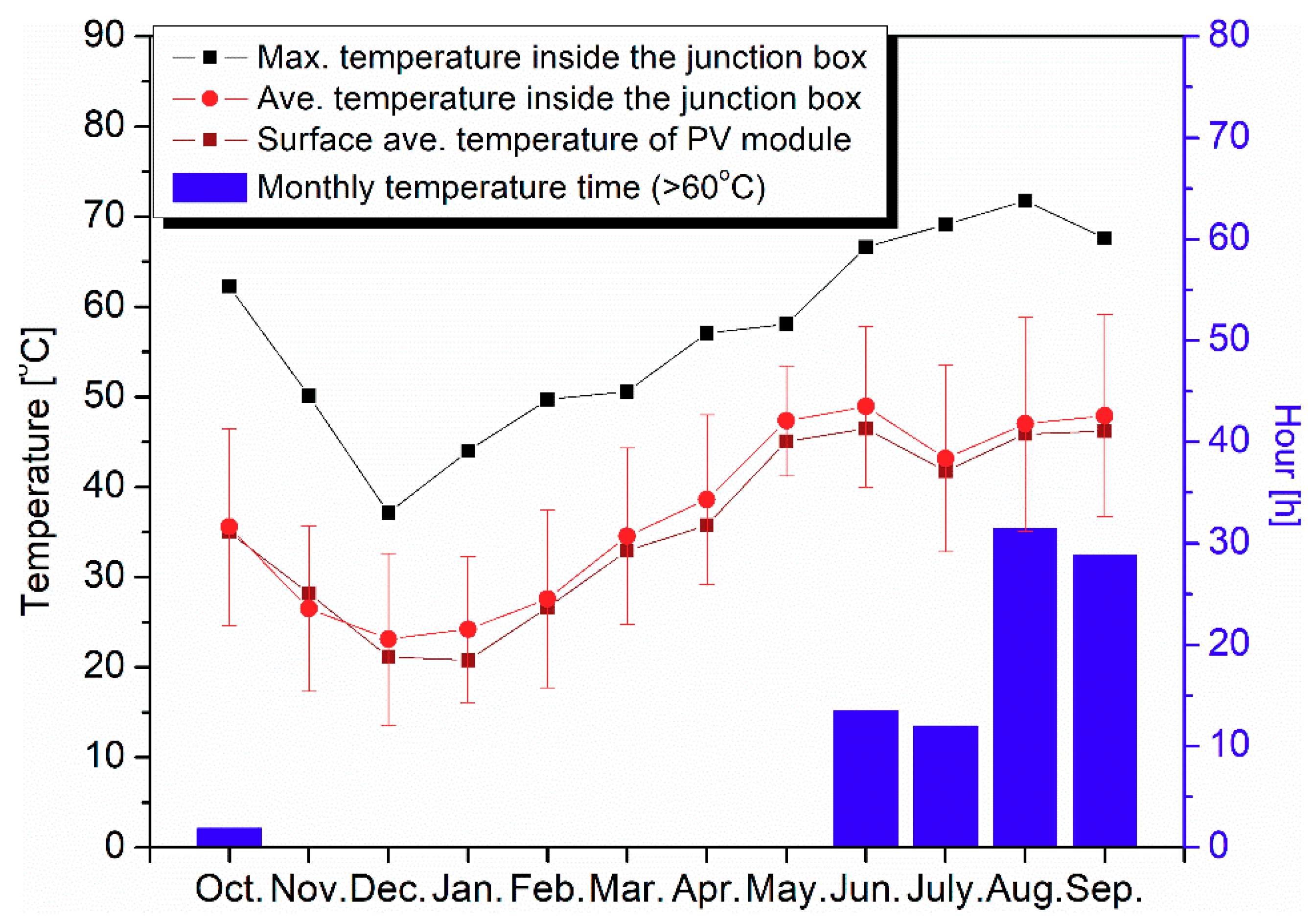
Figure 3.
(a) Schematic diagram and (b) experimental equipment for measuring the current of a bypass diode at various temperatures.
Figure 3.
(a) Schematic diagram and (b) experimental equipment for measuring the current of a bypass diode at various temperatures.
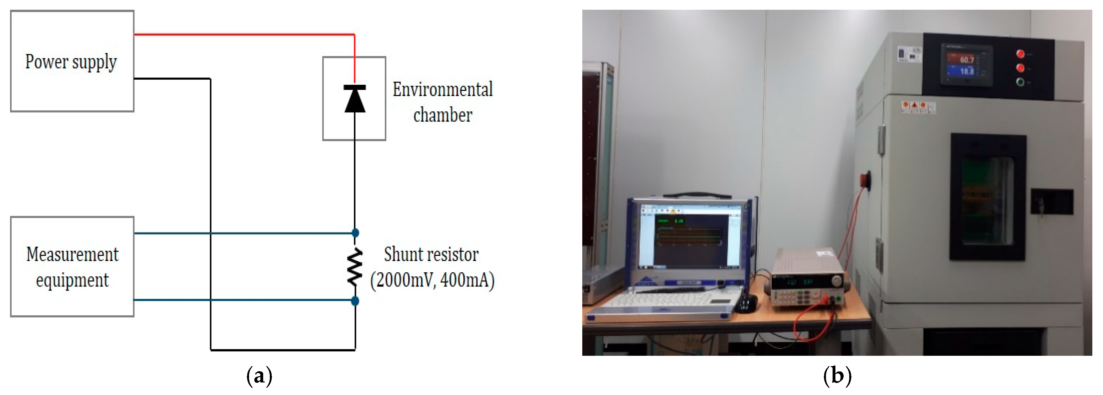
Figure 4.
Leakage current of the bypass diode at various temperature and reverse bias voltage: (a) 10 V, (b) 15 V, and (c) 20 V. (d) The leakage current of the bypass diode as a function of reverse bias voltage with different surrounding temperatures.
Figure 4.
Leakage current of the bypass diode at various temperature and reverse bias voltage: (a) 10 V, (b) 15 V, and (c) 20 V. (d) The leakage current of the bypass diode as a function of reverse bias voltage with different surrounding temperatures.
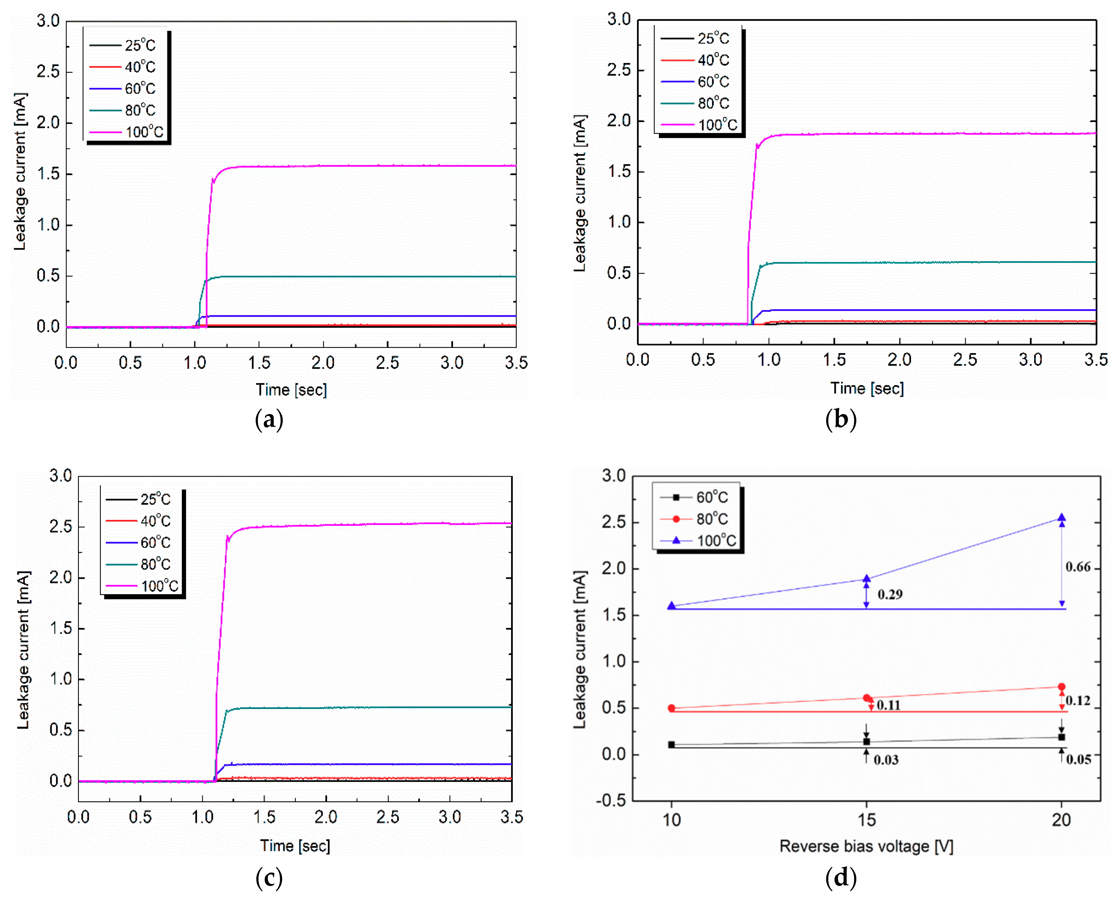
Figure 5.
IR images of bypass diode failure in the field (Ti27, FLUKE Co, Ltd.).

Figure 6.
Measured I–V curves of the normal and failed bypass diode.

Figure 7.
X-ray analysis images (a) normal bypass diode, (b) failed bypass diode.
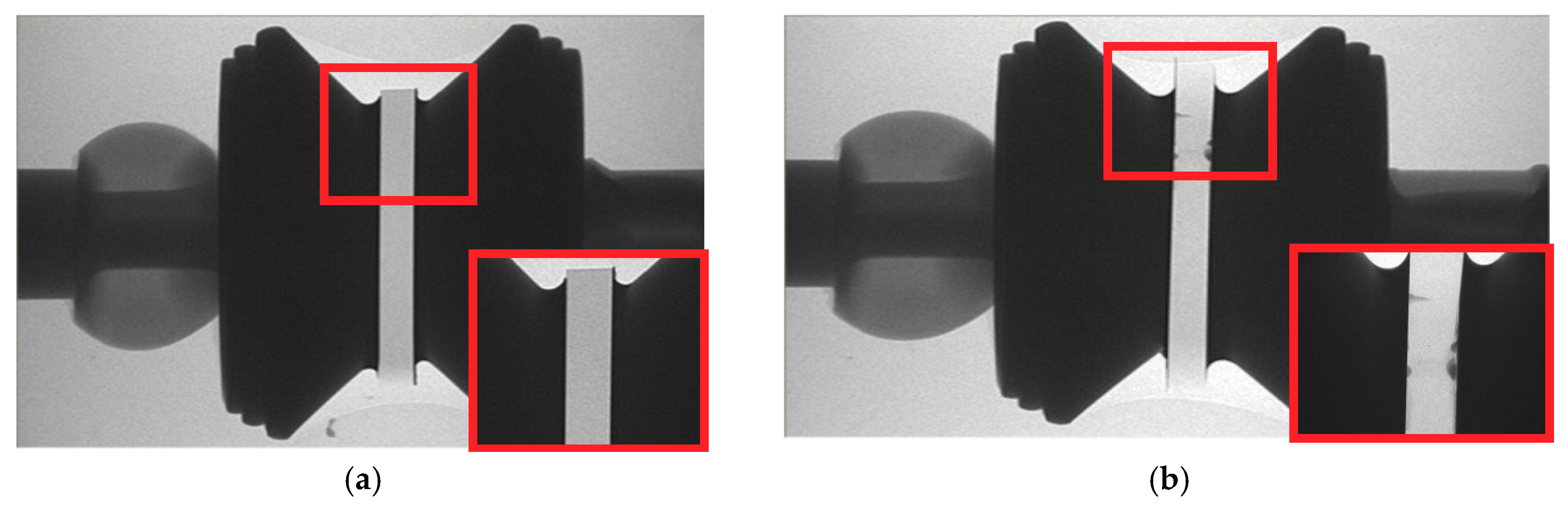
Figure 8.
Cross-sectional images of (a) normal and (b) failed bypass diodes observed using optical microscope (×25).
Figure 8.
Cross-sectional images of (a) normal and (b) failed bypass diodes observed using optical microscope (×25).
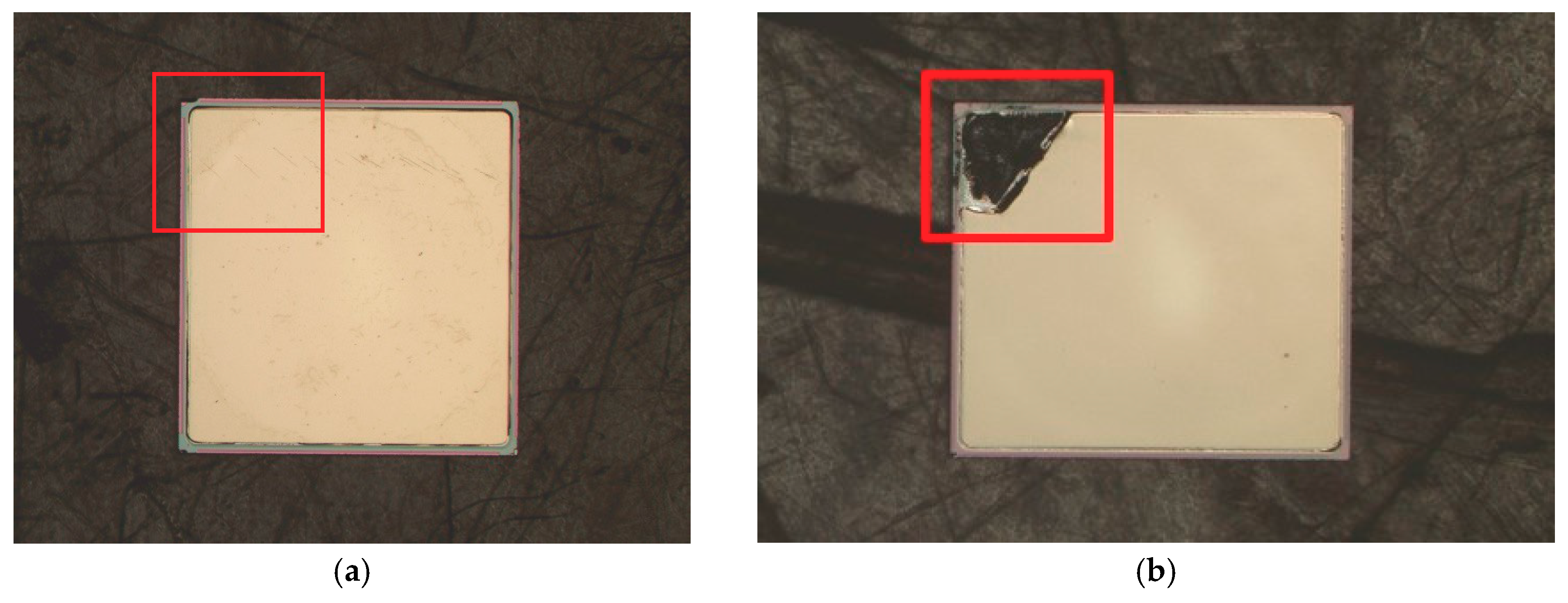
Figure 9.
Magnified images (×200) of (a) normal and (b) failed bypass diode.


Table 1.
Measured peak average leakage current.
| Peak Average Leakage Current (mA) | |||
|---|---|---|---|
| Temperature. | 10 V | 15 V | 20 V |
| 25 °C | 0.01 | 0.01 | 0.02 |
| 40 °C | 0.04 | 0.04 | 0.05 |
| 60 °C | 0.11 | 0.14 | 0.19 |
| 80 °C | 0.50 | 0.61 | 0.73 |
| 100 °C | 1.60 | 1.89 | 2.55 |
© 2018 by the authors. Licensee MDPI, Basel, Switzerland. This article is an open access article distributed under the terms and conditions of the Creative Commons Attribution (CC BY) license (http://creativecommons.org/licenses/by/4.0/).
Share and Cite
MDPI and ACS Style
Shin, W.G.; Ko, S.W.; Song, H.J.; Ju, Y.C.; Hwang, H.M.; Kang, G.H. Origin of Bypass Diode Fault in c-Si Photovoltaic Modules: Leakage Current under High Surrounding Temperature. Energies 2018, 11, 2416. https://doi.org/10.3390/en11092416
AMA Style
Shin WG, Ko SW, Song HJ, Ju YC, Hwang HM, Kang GH. Origin of Bypass Diode Fault in c-Si Photovoltaic Modules: Leakage Current under High Surrounding Temperature. Energies. 2018; 11(9):2416. https://doi.org/10.3390/en11092416
Chicago/Turabian StyleShin, Woo Gyun, Suk Whan Ko, Hyung Jun Song, Young Chul Ju, Hye Mi Hwang, and Gi Hwan Kang. 2018. "Origin of Bypass Diode Fault in c-Si Photovoltaic Modules: Leakage Current under High Surrounding Temperature" Energies 11, no. 9: 2416. https://doi.org/10.3390/en11092416
Note that from the first issue of 2016, this journal uses article numbers instead of page numbers. See further details here.