The Parallel Virtual Infinite Capacitor Applied to DC-Link Voltage Filtering for Wind Turbines


1
School of Engineering, University of Warwick, Coventry CV4 7AL, UK
2
School of Electrical Engineering, Tel Aviv University, P.O. Box 39040, Tel Aviv, Israel
*
Author to whom correspondence should be addressed.
Energies 2018, 11(7), 1649; https://doi.org/10.3390/en11071649
Submission received: 17 April 2018
/
Revised: 4 June 2018
/
Accepted: 20 June 2018
/
Published: 25 June 2018
(This article belongs to the Section F: Electrical Engineering)
Abstract
:We propose the parallel virtual infinite capacitor (PVIC) concept, which refers to two virtual infinite capacitors (VIC) connected to the same DC link and sharing one capacitor, one tuned to low frequencies (LF) and one tuned to high frequencies (HF). A PVIC can suppress voltage variations (ripple) in a wider frequency range than a usual VIC. The LF-VIC is controlled by a sliding mode controller to regulate the low-frequency component of the voltage to its reference value, and by a proportional-integral (PI) controller to maintain its state of charge within the desired operating range and achieve the ‘plug-and-play’ pattern of PVIC. The HF-VIC is controlled by another sliding mode controller to limit the high-frequency ripples and also to keep its state of charge within a reasonable operating interval. As our main application, we use the PVIC to replace a DC-link capacitor for voltage filtering on the DC link of a doubly fed induction generator (DFIG), which is driven by a WindPact (WP) 1.5-MW wind turbine under different grid conditions with turbulent wind input. The simulation study indicates that the PVIC provides much better voltage stabilisation than a DC-link capacitor with the same capacitance, especially in the low frequency range.
1. Introduction
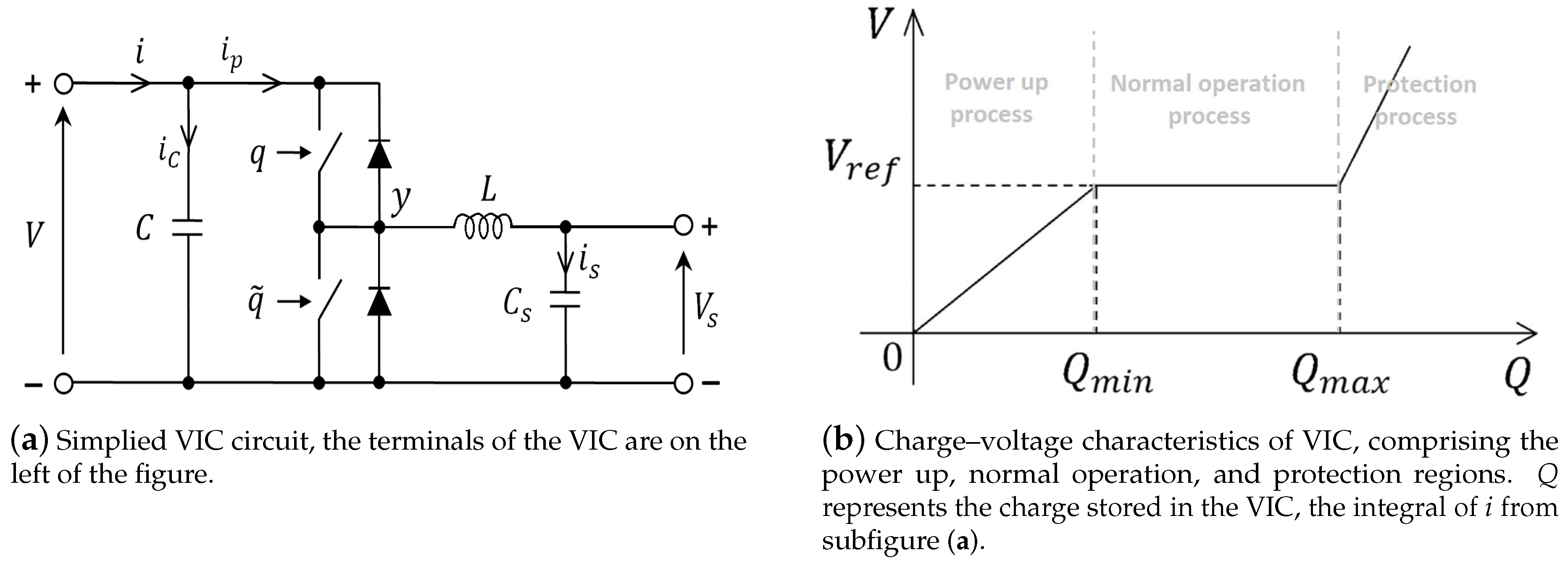
Capacitors are commonly used for DC voltage smoothing (ripple elimination) in power electronic circuits, such as in photovoltaic systems, fuel cells, LED drivers, electric (or hybrid) vehicles and their chargers, power factor correctors (PFC), the power train of wind power generators, etc. Low-frequency ripple suppression requires large capacitance, which could be provided by electrolytic or super-capacitors. However, such capacitors suffer from low reliability and low operating voltages [1,2,3]. Many ideas have been proposed as alternatives to large capacitors (or to achieve better performance with the same capacitance), and such circuits are known as “power filters”, “active capacitors” or “ripple eliminators” (see, for instance, [4,5] (for the output voltage variations of controlled rectifiers) Refs. [6,7] (using stacked swithed capacitors for LED drivers), Refs. [8,9,10,11] and there are many more). We refer to [10,12] for nice surveys of this area. In this line of research, the virtual infinite capacitor (VIC) concept has been introduced in [13], which is a circuit able to eliminate random low-frequency voltage fluctuations [13,14,15]. The idea is to create a nonlinear capacitor where the plot of voltage as a function of charge has a flat segment, where the dynamic capacitance is infinity (see Figure 1b).
The VIC circuit contains a bidirectional DC–DC converter which (using the terminology from Kassakian et al. [16]) is a canonical switching cell (see Figure 1a for a simplified circuit not showing sensing, control or drivers). In [17], the control algorithm and operation of the VIC have been redesigned to work in discontinuous conduction mode (DCM), which has enabled substantially reducing the switching frequency (and using snubber circuits to reduce the switching losses). As can be seen in Figure 1b, there are three regions of operation for the VIC. The control algorithms are designed individually for these three regions. The most important is the normal operating range (the middle segment in Figure 1b) where the voltage V across the VIC remains at a reference value , while the charge Q can vary in the interval . In this range, the gate control signals q and are controlled in such a way as to transfer the excess charge that would create voltage ripples in V to the capacitor and thus constrain the voltage V to a small neighbourhood of . This VIC configuration was found to be quite effective in suppressing unpredictable voltage fluctuations, through both simulations [17,18] and experiments [15,19].
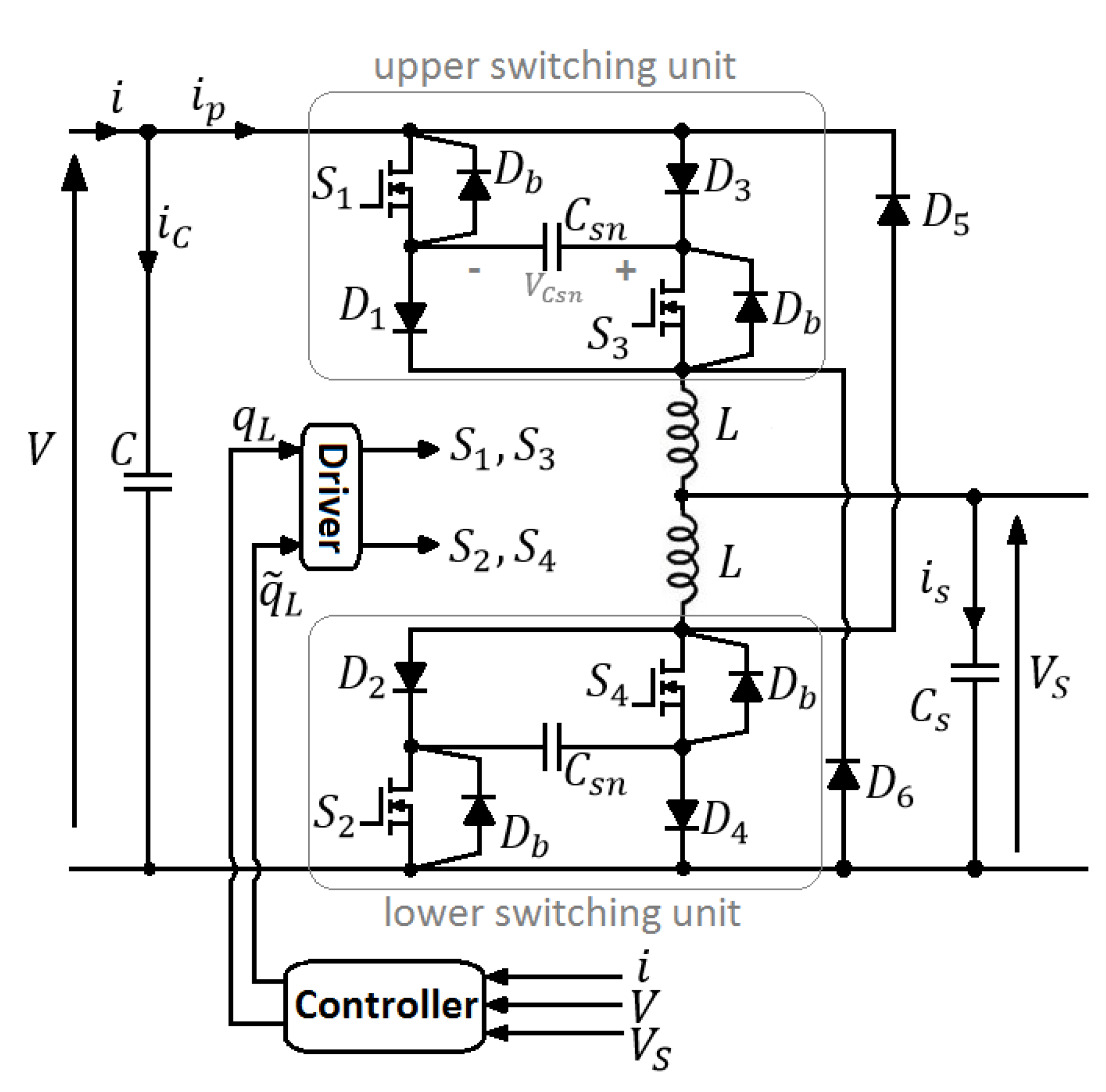
When we compute the output impedance of a VIC (as is done, for instance, in [15]), we find that it is high for frequencies near zero (as it should), it has a region where it is very low (as desired), but it grows for higher frequencies. The region of low impedance depends on the control algorithm. There are applications where there are two main sources of ripple, in two distinct frequency ranges. For instance, in the power conversion system of a wind turbine, the DC-link voltage ripple can originate from variations of wind speed (low frequency), grid imbalance (twice the grid frequency) and switching ripple from the main converters (relatively high frequency). To deal with such situations, we introduce here the parallel virtual infinite capacitor (PVIC) concept. The PVIC is composed of two VICs, one for low-frequency (LF) and one for high frequency (HF), which share a common capacitor. We also propose a new soft switching topology (see Figure 2) to be used for both the LF-VIC and the HF-VIC, which of course improves the efficiency compared with earlier designs. The operation of this new circuit will be explained in Section 2. For the LF-VIC, we design a sliding mode controller (SMC) to regulate the DC-link voltage in the frequency range of this VIC. A proportional-integral (PI) controller is used to maintain the charge in this VIC in its normal operating range and realise the ‘plug-and-play’ feature of the PVIC. Another sliding mode controller is designed for the HF-VIC to suppress the high-frequency component of the ripple voltage and at the same time to keep the state of charge (SoC) of this VIC within the normal operating range. Note that sliding mode controllers are robust and appropriate for nonlinear variable structure systems [20,21,22,23] such as power converters [24,25,26,27,28].
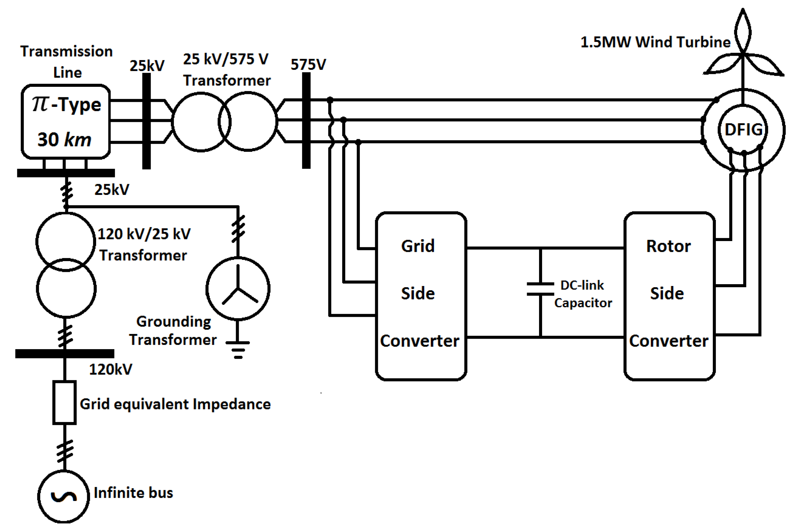
The PVIC can be applied to many systems where voltage filtering in a wide frequency range is required. In this paper, a wind power generator is chosen to demonstrate the performance of the PVIC. Wind power will continue to be an important source of electric power. At the end of 2017, the cumulative installed wind turbine capacity was over 539 GW, which can cover over 5% of the electric power demand of the world. Wind power capacity is expected to rise to 840 GW in 2020 [29,30]. Doubly fed induction generators (DFIG) have been widely used for wind turbines with power ratings of 1.5-MW and above since 1996 [31]. In this paper, the PVIC is used for DC-link voltage filtering on the DC link of a 1.5-MW DFIG wind turbine system.
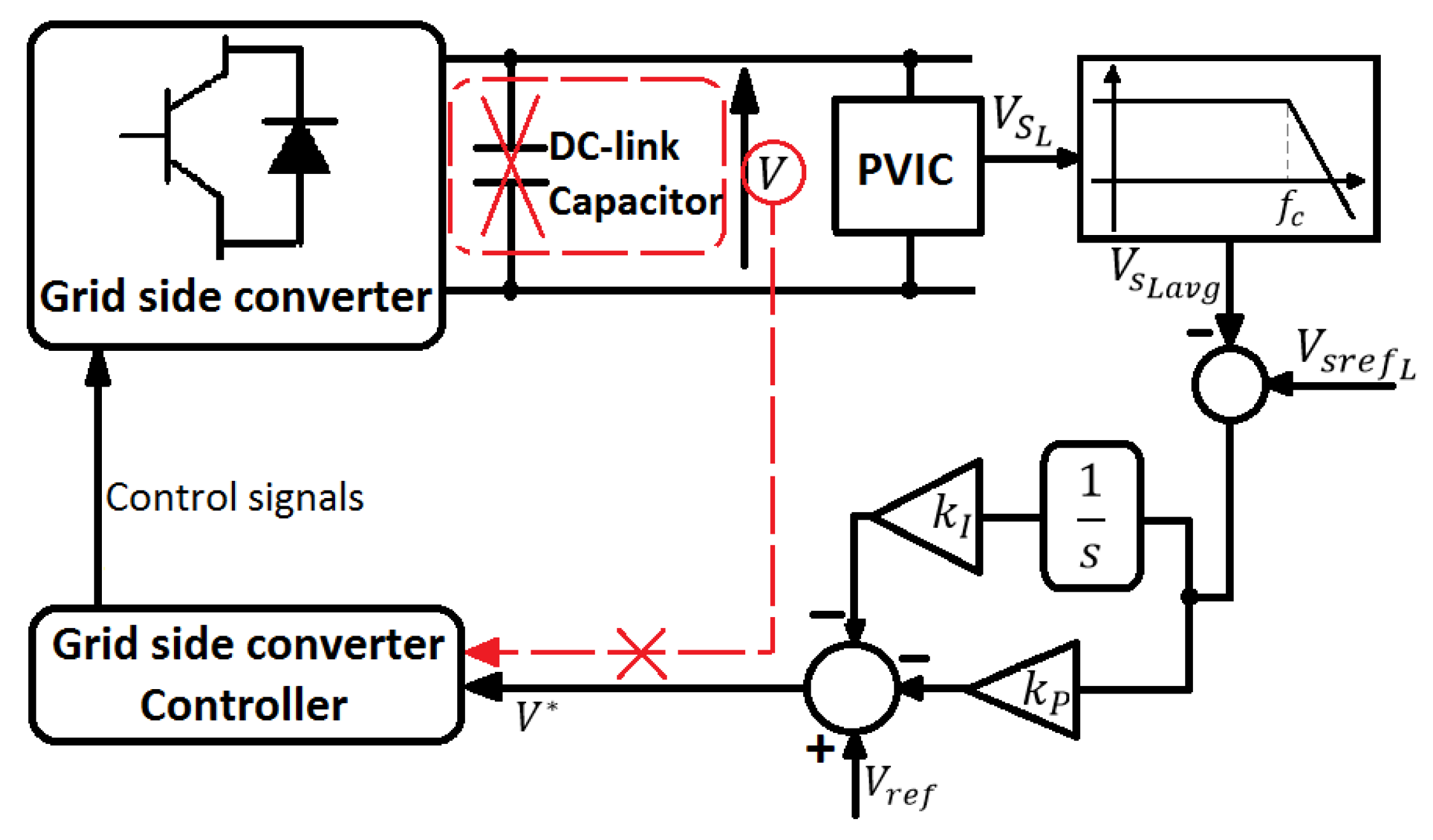
A DFIG wind turbine is quite vulnerable to grid faults because the DFIG stator is directly connected to the grid. Grid faults may cause voltage variations at the DFIG terminals, which may lead to high currents causing the DC-link voltage to drop, preventing the converters from working, or to rise too high, which may damage the capacitors and IGBTs [32,33]. During grid faults, the DC-link voltage should be maintained at the normal level to enable the converters to apply the voltage ride through an algorithm, especially to guarantee the control performance of the rotor side converter. Even without grid faults, DC-link voltage fluctuations need to be limited to guarantee accurate power regulation [33]. PVIC serves as a solution to maintain the DC-link voltage within reasonable bounds, regardless of the grid conditions. Different electronic circuits used for active ripple suppression on the DC link of wind turbine have been proposed (see [34,35] and the references therein). Figure 3 shows the configuration of a DFIG driven by a 1.5-MW wind turbine connected to the power grid via back-to-back converters and transformers. Typically, the rotor side converter is controlled to maximize wind power extraction, and the grid side converter is controlled to stabilise the DC-link voltage.
In this paper, we use a grid-connected DFIG model [36,37], driven by the popular WindPact (WP) 1.5-MW wind turbine [38,39,40] under turbulent wind generated by NREL Turbsim [41]. We have replaced the DC-link capacitor seen in Figure 3 with a PVIC with the same total capacitance and we compare the performance of the DC-link capacitor with that of the PVIC in stabilizing the DC-link voltage. The comparisons under different grid faults demonstrate the capability of the PVIC in handling unpredictable voltage fluctuations. In order to introduce disturbances to the DC link, we have simulated faults at the infinite bus. The simulations indicate that the PVIC is more effective in suppressing the voltage fluctuations than the equivalent DC-link capacitor (i.e., a DC-link capacitor with the same capacitance), regardless if there are grid disturbances or not.
The structure of the paper is as follows. In Section 2, we briefly explain the operation principle and control of the VIC and especially of the soft switching version from Figure 2. In Section 3, we present our simulation results for the the DC-link voltage filtering performance of the PVIC. We compare the performance of the PVIC with that of the equivalent (in capacitance) DC-link capacitor.
2. The PVIC and Its Control
To improve efficiency, we use a new soft switching circuit shown in Figure 2, where the two snubber capacitors are small. This is an improvement of the circuit appearing in ([42], Figure 2). The upper switching unit is composed of the , , , and , in which is synchronized with . The lower switching unit is similar. The inductors are not coupled.
We take the upper switching unit (see Figure 2) as an example to explain the soft switching mechanism. This is really soft switching only in discontinuous conduction mode (DCM), while in continuous conduction mode (CCM) it is only zero voltage switching-off. Immediately after and are turned off, the voltage on the left side of will remain close to V without dropping abruptly because takes time to get charged via and until reaches V, which implies zero voltage switching-off of and . The main current will flow via , decreasing at a slope of , until one of the following two events occurs: either the current reaches zero and then remains zero for some time (DCM) or the switches are controlled to turn on again. Immediately after and are turned on, the voltage on the right side of will suddenly jump to . Then, starts to release energy through the switches and the upper inductor L to charge , until reaches nearly zero or the switches are controlled to turn off. This discharging period of is relatively short because the time constant is small. Hence, practically all the energy that was stored in is saved into . However, if the inductor current at the moment of switching-on is not zero, then we do not have zero current switch-on. After switch-on and after is emptied, the inductor current (flowing through the switches and the diodes D1 and D3) grows, at a slope of . Of course, the rising current will stop once the switches are turned off, which closes the whole cycle. The story for the lower switching unit is similar.
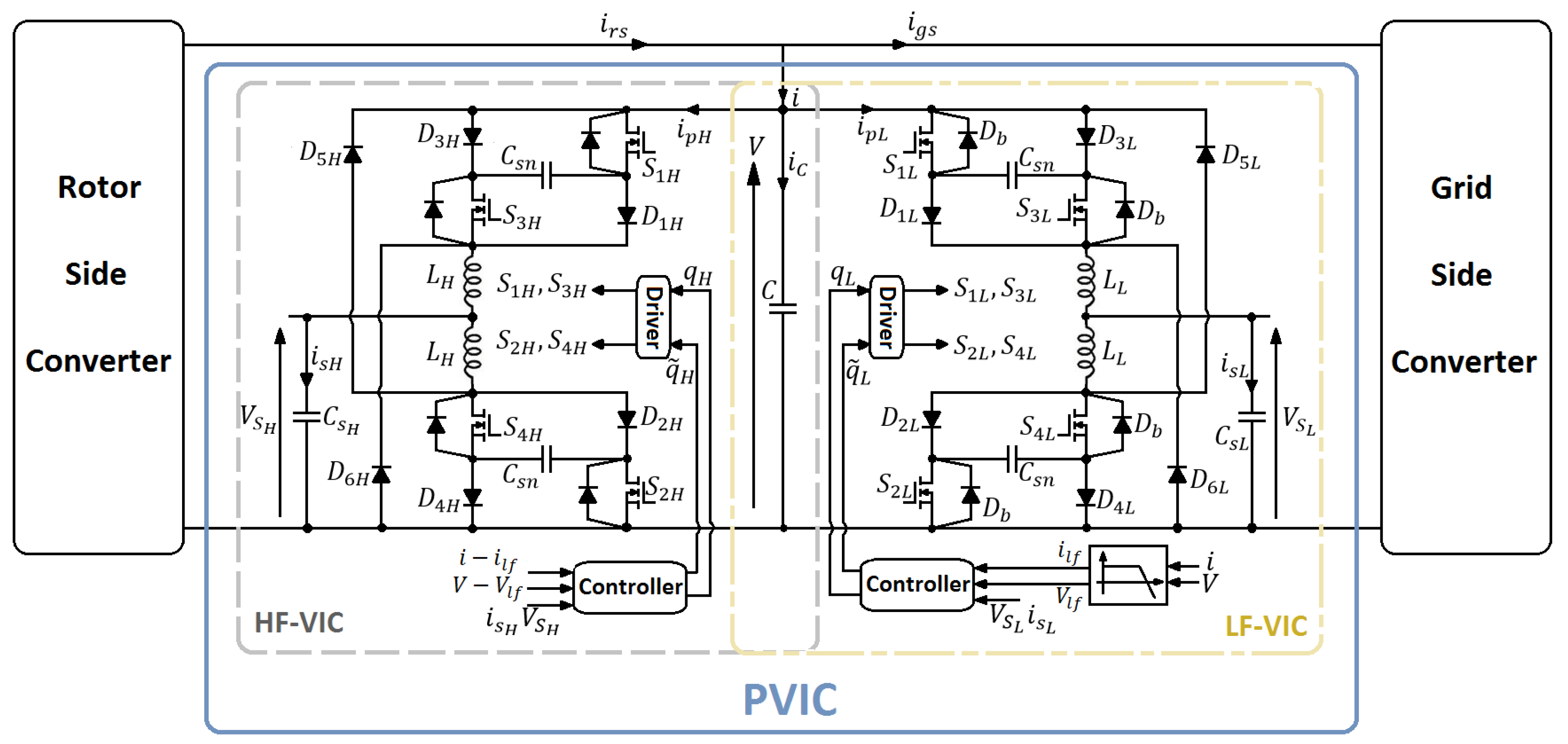
Figure 4 shows the circuit realisation of a PVIC, which replaces the DC-link capacitor. are binary signals, and . The switches and are on if . The switches and are on if . The binary signals and are defined in a similar way. The capacitor is smaller than the capacitor . The remaining components in the HF-VIC are same as in the LF-VIC. The control of PVIC is attained by the LF-VIC controller and HF-VIC controller. The former regulates low-frequency components of the voltage V to the neighbourhood of its reference, while the latter suppresses the high-frequency ripples of the voltage V. During the power up process (see the left segment in Figure 1b), a constant duty cycle and a constant PWM switching frequency are applied to both VICs. During the protection region of operation (the right segment in Figure 1b), all the switches are turned off to avoid the overcharge of and . The transitions between the three processes are controlled using a state machine, which was detailed in [19]. Next, we discuss the control algorithm in the normal operation range.
The low-frequency signals & and high-frequency signals and are acquired by passing V and i through a low pass filter with the corner frequency :
According to Figure 4, we have
Multiplying both sides of (2) with , we get
Then, the state equations of the PVIC can be written as:
These state equations are considered only in the operating range, which is defined by:
Note that and . For subsequent analysis, we set the following lower and upper bounds:
2.1. Control of the LF-VIC
The LF-VIC controller is composed of a sliding mode voltage controller and a PI charge controller. Their control objectives are to control the low-frequency component of the voltage to its expected reference in normal operation process and, restrain the LF-VIC’s SoC within its normal operating range, respectively.
2.1.1. Voltage Control of the LF-VIC
We use a sliding mode controller to regulate the low-frequency component of V. We employ a sliding function with the states and disturbance , based on ([13], Section 6):
where we set . The sliding surface is the set of all the possible for which
Note that the energy stored in the two inductors of the PVIC can be roughly written as . The nonlinear term in (9) represents the energy in . The remaining part , which represents the energy in , is included in the HF-VIC controller, which will be discussed in Section 2.2. The absolute values of and should be small enough to diminish deviation between and when x is controlled to be within .
To reduce chattering effects and limit operating frequencies within a controllable range, we use the hysteresis-modulation (HM) sliding mode control [24] to determine the binary switching signals and :
where is a small positive number. In the stability analysis later, we assume for simplicity but without loss of generality.
The sliding mode controller is designed according to the following steps. Firstly, the hitting condition should be satisfied to ensure that the state trajectory is guided to the sliding surface. After that, when the states are within a small vicinity of the sliding surface, the existence condition needs to be satisfied to maintain the states within the neighbourhood of the sliding surface and always direct the states towards the desired surface [20,25].
In this paper, we describe the hitting condition by
where
When for all , . To satisfy (12), we require that
Here, is set to be . Note that it is hard to limit a current derivative term in reality. This limit is allowed to be violated under some circumstances such as the abrupt current change due to some faults. However, it will be brought back by the control schemes. A sufficient condition for (15) is
When for all , . To satisfy (12), we have
That is, a sufficient condition for (17) is
Then, the existing condition for this SMC is
The parameters and should be chosen to fulfill the inequalities (15), (17), (26), and (27) to satisfy both the hitting condition and existing condition, which are the sufficient conditions to attain the successful control. The details about the selection of and will be discussed in Section 2.3.
2.1.2. Charge Control of the LF-VIC
In the application of grid connected DFIG system, a charge control scheme is developed to regulate the LF-VIC’s state of charge () by coupling a PI controller with the controller of grid side converter. Since the charge controller is required to operate more slowly than the voltage controller, the average of (i.e., ) is controlled, which is acquired by passing through a low pass filter with the corner frequency (see Figure 5). In the voltage control of DC-link capacitor, the voltage V is fed back to the controller of grid side converter. Herein, the voltage rather than V is injected. is the estimated value of V obtained from the LF-VIC’s state of charge through a PI controller:
In this way, the control scheme of the grid side converter is not violated, realising a ‘plug-and-play’ pattern for the PVIC.
2.2. Control of the HF-VIC
For the control of HF-VIC, both voltage control and charge control are implemented by a sliding mode controller whose sliding function is
The sliding surface is the set of all the possible for which
The expression appearing in (28) represents the power stored in , which is included in the HF-VIC controller. is the charge control term in this sliding function. As with the charge control of the LF-VIC, the average of (i.e., ) is regulated to realise a much slower response of the charge control than the voltage control. is obtained by passing through a low pass filter with the corner frequency . The absolute values of the parameters and should be very small to guarantee the accuracy of the control.
The hysteresis-modulation (HM) sliding mode control is also applied to the HF-VIC, using the same as in (11):
The hitting condition is described as
for all . Here, is limited as , where should be small due to the slow change of . Similarly as in Section 2.1, when and , we have
and
respectively. Here, is limited as , that is, the sufficient conditions for (30) and (31) are
and
The parameters and should be chosen to satisfy the inequalities (30), (31), (38) and (39), so that the state trajectory will converge and stabilise at the sliding surface . The details about the selection of and will be discussed in Section 2.3.
2.3. Parameter Selection
In order to limit the deviation between V and its reference , the absolute values of the parameters , , and should be small. We apply the interior-point optimization algorithm to find the boundaries of these four parameters, which are embedded in the nonlinear programming solver ‘fmincon’in Matlab (MathWorks).
The optimization for LF-VIC controller parameters is conducted to minimize under the inequality constraints (7), (8), (15), (17), (19), (26), (27), and equality constraint (10). Similarly, the objective function for parameter optimization of the HF-VIC controller is , with the inequalities constraints (7), (8), (30), (31), (34), (38), (39), and equality constraint (29). The results of these optimizations provide the boundaries for and to ensure the successful control of both LF-VIC controller and HF-VIC controller.
The parameters’ initial values are all set to be zero. The related operating boundaries are listed in Table 1. The optimal boundaries for the parameters are
3. Simulation Study
The simulations are conducted using a grid-connected DFIG model [36,37] driven by the WP 1.5-MW wind turbine model [38,39,40]. The parameters of the DFIG are listed in Table 2. The hub height of wind turbine is 84 m. The rated wind speed is about 12 m/s. The blade length is m and the maximum blade chord is 8% of blade radius [43].
The NREL FAST (Fatigue, Aerodynamics, Structures, and Turbulence) code [38] is used to simulate dynamic responses of the turbine. FAST takes aerodynamics, control and electrical (servo) dynamics, and structural (elastic) dynamics of the turbine into account. FAST is interfaced with Matlab/Simulink through a Simulink S-Function block. During simulations, this block calls the FAST Dynamic Library, which has integrated all the FAST modules [38] and is compiled as a dynamic-link-library (DLL).
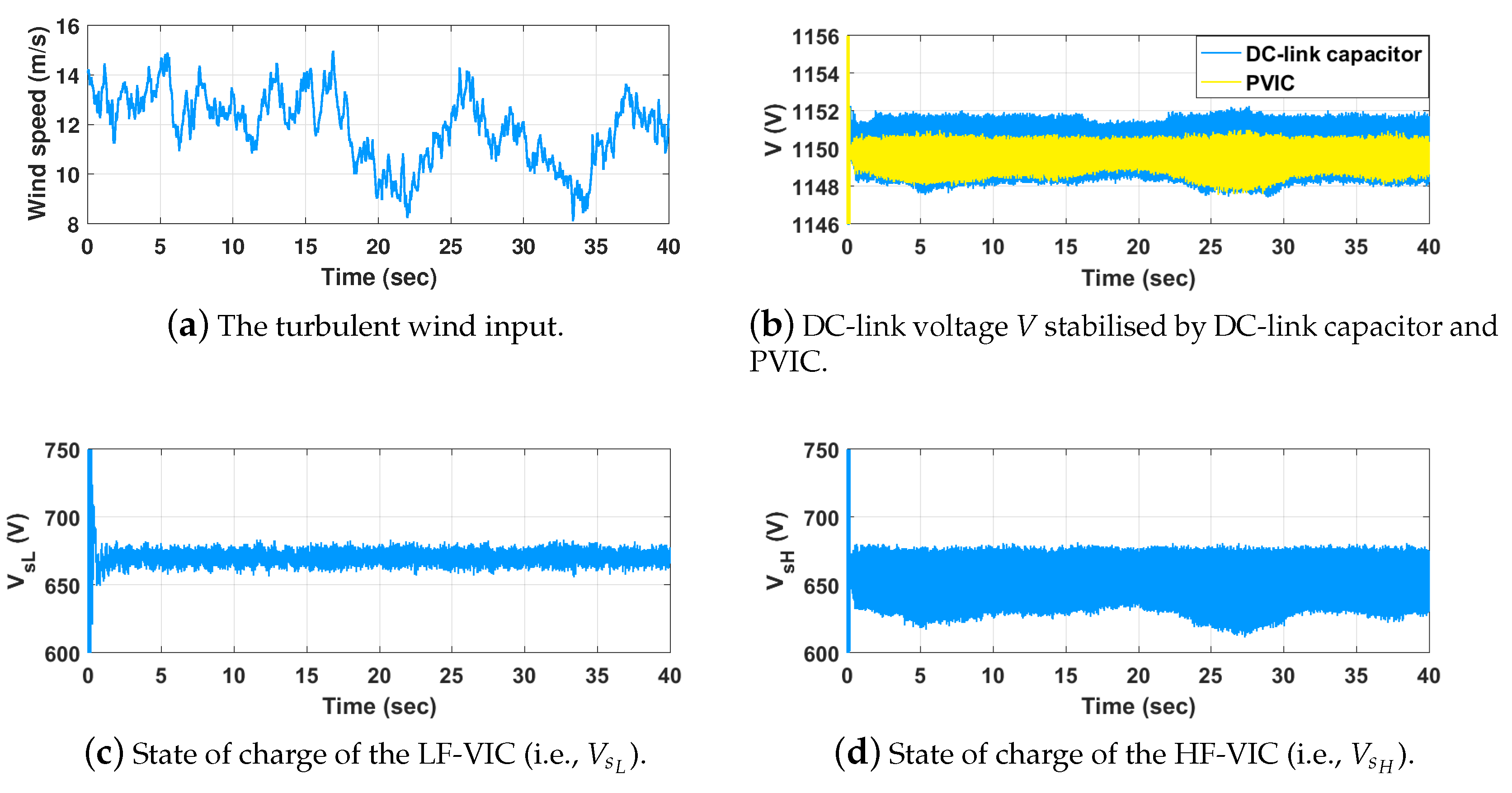
NREL TurbSim [41] is utilised to generate stochastic, full-field, and turbulent wind flows for simulation studies. The International Electro-technical Commission (IEC) Kaimal spectral model [44,45] in Turbsim is applied to generate the wind condition as shown in Figure 6a, with the category A (most turbulent) IEC NTM (normal turbulence model). The mean hub-height longitudinal wind speed is 12 m/s. Note that the average sampling frequency of the LF-VIC controller is smaller than that of HF-VIC controller in the simulations, which are approximately 45 kHz and 100 kHz, respectively.
The voltage filtering performances of two configurations are compared: a 15 mF DC-link capacitor and a PVIC as in Figure 4, where the total capacitance of C, and is 15 mF. Table 3 and Table 4 list the parameters of the electronic components in PVIC and control parameters of PVIC, respectively.
Firstly, the simulation is conducted without grid disturbance under the turbulent wind input (see Figure 6). Figure 6a,b demonstrate the turbulent wind input and the DC-link voltage stabilised by DC-link capacitor and PVIC. Figure 6c,d illustrate the SoC of PVIC (i.e., and ). It is clear that when there is no grid disturbance, both configurations can stabilise the DC-link voltage V to its reference, and PVIC reduces about of the voltage fluctuations compared with the equivalent DC-link capacitor (see Figure 6b), which is mainly achieved by HF-VIC controller to suppress the high-frequency ripple due to the fast switching of two converters. The SoC of the LF-VIC and HF-VIC are successfully controlled to the vicinity of their references by the charge control schemes explained in Section 2.
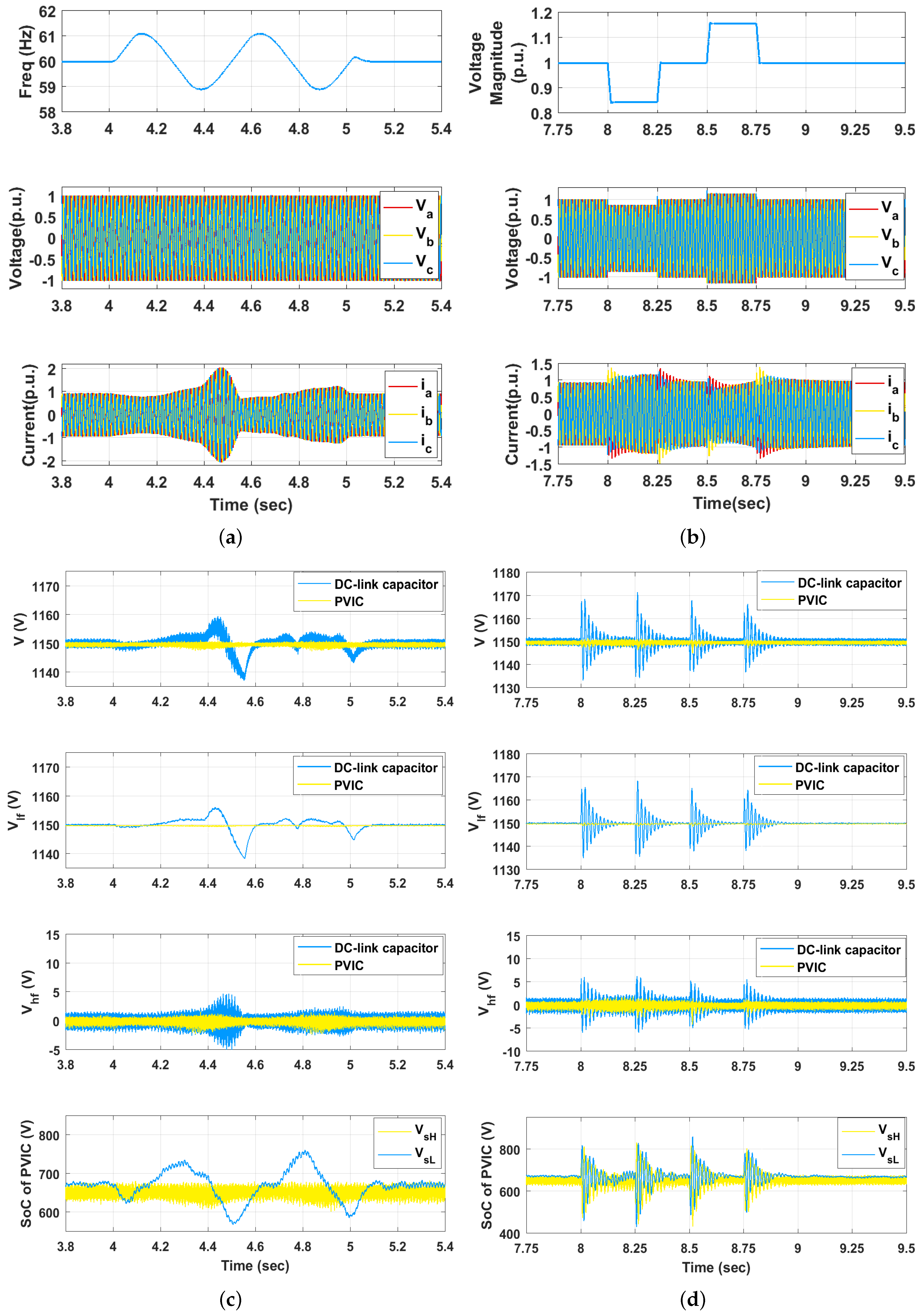
Then, the simulations are conducted under four types of grid disturbances with the same turbulent wind input (Figure 6a). The first case is the frequency variation. In reality, the frequency, as a key factor to judge the power quality, is allowed to vary within a very narrow range during normal operation. Here, we test the performance of the PVIC and a DC-link capacitor under a one-second large sinusoidal grid frequency variation with an amplitude of 1 Hz and a period of s. Figure 7a,c show this grid condition and the performances of PVIC and DC-link capacitor. Note that the and of the DC-link voltage are obtained according to (1).
The second type of the tested grid disturbances is the balanced three-phase voltage sag and swell. This is one of the most common power disturbances, which is usually caused by abrupt reduction or increase in loads. The grid voltage is altered four times by p.u. and each change is kept for 15 grid cycles (250 ms) (see Figure 7b,d).
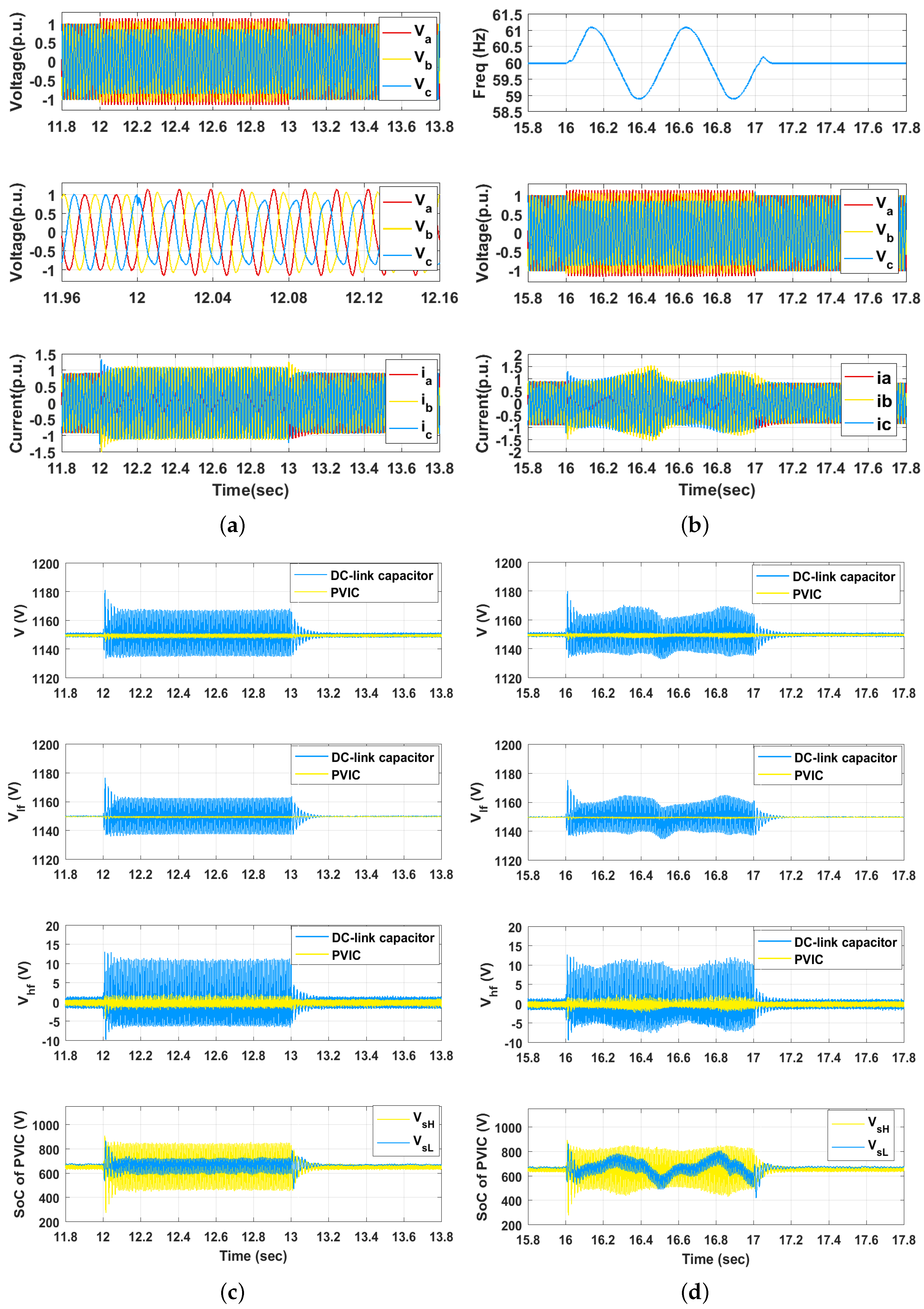
The third case of the disturbance test is the harmonics. In reality, a small range of harmonics due to the nonlinear loads, transformer magnetisation nonlinearities, rectification, etc. is allowed in the power system, which may introduce the high-frequency ripple to DC-link voltage. We inject a combination of a negative-sequence 1st order harmonic (with the magnitude of p.u.) and negative-sequence 3rd order harmonic (with the magnitude of p.u. and phase shift of ), lasting for 1 s. Figure 8a,c show this grid condition and the voltage filtering performance.
Finally, we combine the above frequency variation and harmonic disturbances as the fourth case. That is, both high-frequency and low-frequency ripples are introduced to the DC-link voltage. The grid condition and the voltage filtering performance are shown in Figure 8b,d.
From Figure 7 and Figure 8, it is clear that the PVIC achieves 10–20 times smaller variations in the DC-link voltage than the equivalent DC-link capacitor during these tested grid disturbances. This is because the oscillations in the DC-link voltage are transferred into the capacitors and of the PVIC. The same conclusion can be obtained under other grid conditions, such as unbalanced voltage sag and swell, the phase shift in voltage, different harmonic injections, frequency steps variations, or the combinations of some of these faults.
4. Conclusions
We have introduced the concept of parallel virtual infinite capacitor (PVIC), which refers to a low-frequency (LF) virtual infinite capacitor (VIC) and a high-frequency (HF) VIC working on a common DC link and sharing one capacitor. It is meant to suppress voltage ripple in a wider frequency band than what one VIC could achieve. The low frequency ripple is regulated by a sliding mode controller, and a PI controller is applied to maintain the LF-VIC within its operating range. Another sliding mode controller is applied to suppress high-frequency fluctuations while at the same time keeping the HF-VIC’s state of charge within the normal range. The PVIC has been applied to replace the DC-link capacitor between two back-to-back converters in a grid-connected DFIG wind turbine system. The simulations were conducted under normal grid operation and four types of grid disturbances with turbulent wind (frequency variation, three-phase voltage sag and swell, harmonics and frequency variation with harmonics). The results indicate that the PVIC provides outstanding ripple suppression performance regardless of the low-frequency and high-frequency fluctuations, individually or together. In comparison with an equivalent DC-link capacitor, the PVIC reduces the DC-link voltage ripple by about 30% during normal grid operation, and approximately 10–20 times during the tested grid disturbances. The PVIC can also be applied to other systems that have a large capacitor for voltage filtering, such as PFC, photovoltaic power generators, vehicle chargers, etc.
Author Contributions
S.L. made the major contribution. All the other authors contributed equally to this paper.
Funding
The visits of G.W. to the UK were supported by a fellowship from the Leverhulme Trust.
Conflicts of Interest
The authors declare no conflict of interest.
References
- Kötz, R.; Carlen, M. Principles and applications of electrochemical capacitors. Electrochim. Acta 2000, 45, 2483–2498. [Google Scholar] [CrossRef]
- Burke, A. Ultracapacitors: Why, how, and where is the technology. J. Power Sources 2000, 91, 37–50. [Google Scholar] [CrossRef]
- Conway, B.E. Electrochemical Supercapacitors: Scientific Fundamentals and Technological Applications; Springer Science & Business Media: New York, NY, USA, 2013. [Google Scholar]
- Cao, X.; Zhong, Q.C.; Ming, W.L. Ripple eliminator to smooth DC-bus voltage and reduce the total capacitance required. IEEE Trans. Ind. Electron. 2015, 62, 2224–2235. [Google Scholar] [CrossRef]
- Zhong, Q.C.; Ming, W.L.; Cao, X.; Krstic, M. Control of ripple eliminators to improve the power quality of DC systems and reduce the usage of electrolytic capacitors. IEEE Access 2016, 4, 2177–2187. [Google Scholar] [CrossRef]
- Chen, M.; Afridi, K.K.; Perreault, D.J. Stacked switched capacitor energy buffer architecture. IEEE Trans. Power Electron. 2013, 28, 5183–5195. [Google Scholar] [CrossRef]
- Ni, Y.; Pervaiz, S.; Chen, M.; Afridi, K.K. Energy density enhancement of stacked switched capacitor energy buffers through capacitance ratio optimization. IEEE Trans. Power Electron. 2017, 32, 6363–6380. [Google Scholar] [CrossRef]
- Xia, Y.; Ayyanar, R. Adaptive DC link voltage control scheme for single phase inverters with dynamic power decoupling. In Proceedings of the 2016 IEEE Energy Conversion Congress and Exposition (ECCE), Milwaukee, WI, USA, 18–22 September 2016; pp. 1–7. [Google Scholar]
- Qin, S.; Lei, Y.; Barth, C.; Liu, W.C.; Pilawa-Podgurski, R.C. A high power density series-stacked energy buffer for power pulsation decoupling in single-phase converters. IEEE Trans. Power Electron. 2017, 32, 4905–4924. [Google Scholar] [CrossRef]
- Sun, Y.; Liu, Y.; Su, M.; Xiong, W.; Yang, J. Review of active power decoupling topologies in single-phase systems. IEEE Trans. Power Electron. 2016, 31, 4778–4794. [Google Scholar] [CrossRef]
- Cai, W.; Jiang, L.; Liu, B.; Duan, S.; Zou, C. A power decoupling method based on four-switch three-port DC/DC/AC converter in DC microgrid. IEEE Trans. Ind. Appl. 2015, 51, 336–343. [Google Scholar] [CrossRef]
- Hu, H.; Harb, S.; Kutkut, N.; Batarseh, I.; Shen, Z. A review of power decoupling techniques for microinverters with three different decoupling capacitor locations in PV systems. IEEE Trans. Power Electron. 2013, 28, 2711–2726. [Google Scholar] [CrossRef]
- Yona, G.; Weiss, G. The virtual infinite capacitor. Int. J. Control 2017, 90, 78–89. [Google Scholar] [CrossRef]
- Yona, G.; Weiss, G. Zero-voltage switching implementation of a virtual infinite capacitor. In Proceedings of the 2015 IEEE 5th International Conference on Power Engineering, Energy and Electrical Drives (POWERENG), Riga, Latvia, 11–13 May 2015; pp. 157–163. [Google Scholar]
- Lin, J.; Weiss, G. Plug-and-play realization of the virtual infinite capacitor. In Proceedings of the 2017 International Symposium on Power Electronics (Ee), Novi Sad, Serbia, 19–21 October 2017. [Google Scholar]
- Kassakian, J.; Schlecht, M.; Verghese, G. Principles of Power Electronics; Addison-Wesley: Reading, MA, USA, 1992; Chapter 6. [Google Scholar]
- Lin, S.; Lin, J.; Weiss, G.; Zhao, X. Control of a virtual infinite capacitor used to stabilize the output voltage of a PFC. In Proceedings of the 2016 IEEE International Conference on the Science of Electrical Engineering (ICSEE), Eilat, Israel, 16–18 November 2016. [Google Scholar]
- Lin, J.; Weiss, G. The Virtual Infinite Capacitor-Based Active Submodule for MMC. In Proceedings of the 2016 IEEE International Conference on the Science of Electrical Engineering (ICSEE), Eilat, Israel, 16–18 November 2016. [Google Scholar]
- Lin, S.; Qi, P.; Lin, J.; Zhao, X.; Weiss, G.; Ran, L. Experimental ripple suppression performance of a virtual infinite capacitor. In Proceedings of the 2017 International Conference on Applied Electronics (AE), Pilsen, Czech Republic, 5–6 September 2017. [Google Scholar]
- Edwards, C.; Spurgeon, S. Sliding Code Control: Theory and Applications; CRC Press: Boca Raton, FL, USA, 1998. [Google Scholar]
- Perruquetti, W.; Barbot, J.P. Sliding Mode Control in Engineering; CRC Press: Boca Raton, FL, USA, 2002. [Google Scholar]
- Utkin, V. Variable structure systems with sliding modes. IEEE Trans. Autom. Control 1977, 22, 212–222. [Google Scholar] [CrossRef]
- Utkin, V.; Guldner, J.; Shi, J. Sliding Mode Control in Electro-Mechanical Systems; CRC Press: Boca Raton, FL, USA, 2009. [Google Scholar]
- Tan, S.C.; Lai, Y.M.; Tse, C.K. Sliding Mode Control of Switching Power Converters: Techniques and Implementation; CRC Press: Boca Raton, FL, USA, 2011. [Google Scholar]
- Tan, S.C.; Lai, Y.M.; Chi, K.T. General design issues of sliding-mode controllers in DC–DC converters. IEEE Trans. Ind. Electron. 2008, 55, 1160–1174. [Google Scholar]
- Wai, R.J.; Shih, L.C. Design of voltage tracking control for DC–DC boost converter via total sliding-mode technique. IEEE Trans. Ind. Electron. 2011, 58, 2502–2511. [Google Scholar] [CrossRef]
- Alaa, H.; Eric, B.; Pascal, V.; Guy, C.; Gerard, R. Sliding mode control of boost converter: Application to energy storage system via supercapacitors. In Proceedings of the 2009 13th European Conference on Power Electronics and Applications, Barcelona, Spain, 8–10 September 2009. [Google Scholar]
- Gee, A.; Robinson, F.V.; Dunn, R.W. Sliding-mode control, dynamic assessment and practical implementation of a bidirectional buck/boost DC-to-DC converter. In Proceedings of the 14th European Conference on Power Electronics and Applications (EPE 2011), Birmingham, UK, 30 August–1 September 2011. [Google Scholar]
- World Wind Energy Association, Wind Power Capacity Reaches 539 GW, 52.6 GW Added in 2017. Available online: http://www.wwindea.org/2017-statistics/ (accessed on 22 June 2018).
- Global Wind Energy Council, Global Wind Report, Annual Market Update 2017. Available online: http://files.gwec.net/files/GWR2017.pdf (accessed on 22 June 2018).
- Polinder, H.; Ferreira, J.A.; Jensen, B.; Abrahamsen, A.; Atallah, K.; McMahon, R. Trends in wind turbine generator systems. IEEE J. Emerg. Sel. Top. Power Electron. 2013, 1, 174–185. [Google Scholar] [CrossRef]
- Mohammadi, J.; Afsharnia, S.; Vaez-Zadeh, S. Efficient fault-ride-through control strategy of DFIG-based wind turbines during the grid faults. Energy Convers. Manag. 2014, 78, 88–95. [Google Scholar] [CrossRef]
- Yao, J.; Li, H.; Liao, Y.; Chen, Z. An improved control strategy of limiting the DC-link voltage fluctuation for a doubly fed induction wind generator. IEEE Trans. Power Electron. 2008, 23, 1205–1213. [Google Scholar]
- Hu, Y.; Zhu, Z.Q.; Odavic, M. An improved method of DC bus voltage pulsation suppression for asymmetric wind power PMSG systems with a compensation unit in parallel. IEEE Trans. Energy Convers. 2017, 32, 1231–1239. [Google Scholar] [CrossRef]
- Onge, X.F.S.; McDonald, K.; Richard, C.; Saleh, S.A. A new multi-port active DC-link for PMG-based WECSs. In Proceedings of the 2018 IEEE/IAS 54th Industrial and Commercial Power Systems Technical Conference (I&CPS), Niagara Falls, ON, Canada, 7–10 May 2018. [Google Scholar]
- Miller, N.W.; Price, W.W.; Sanchez-Gasca, J.J. Dynamic Modeling of GE 1.5 and 3.6 Wind Turbine-Generators; Technical Report, GE-Power Systems Energy Consulting; General Electric International, Inc.: Schenectady, NY, USA, 2003. [Google Scholar]
- Miller, N.W.; Sanchez-Gasca, J.J.; Price, W.W.; Delmerico, R.W. Dynamic modeling of GE 1.5 and 3.6 MW wind turbine generators for stability simulations. In Proceedings of the 2003 IEEE Power Engineering Society General Meeting (IEEE Cat. No.03CH37491), Toronto, ON, Canada, 13–17 July 2003; Volume 3, pp. 1977–1983. [Google Scholar]
- Jonkman, J.; Buhl, M.L. Fast User’s Guide; NREL Technical Report; National Renewable Energy Laboratory: Golden, CO, USA, 2005. [Google Scholar]
- Singh, M.; Muljadi, E.; Jonkman, J.; Gevorgian, V.; Girsang, I.; Dhupia, J. Simulation for Wind Turbine Generators—With FAST and MATLAB-Simulink Modules; Technical Report; National Renewable Energy Laboratory (NREL): Golden, CO, USA, 2014. [Google Scholar]
- Malcolm, D.; Hansen, A. WindPACT Turbine Rotor Design Study: June 2000–June 2002 (Revised); Technical Report; National Renewable Energy Laboratory (NREL): Golden, CO, USA, 2006. [Google Scholar]
- Jonkman, B.J. TurbSim User’s Guide: Version 1.50; Technical Report; National Renewable Energy Laboratory (NREL): Golden, CO, USA, 2009. [Google Scholar]
- Conrad, M.; DeDoncker, R.W. Avoiding reverse recovery effects in super junction MOSFET based half-bridges. In Proceedings of the 2015 IEEE 6th International Symposium on Power Electronics for Distributed Generation Systems (PEDG), Aachen, Germany, 22–25 June 2015. [Google Scholar]
- Rinker, J.; Dykes, K. WindPACT Reference Wind Turbines; National Renewable Energy Laboratory (NREL): Golden, CO, USA, 2018. Available online: https://www.nrel.gov/docs/fy18osti/67667.pdf (accessed on 22 June 2018).
- International Electrotechnical Commission. Wind Turbine Generator Systems—Part 1: Safety Requirements, 2nd ed.; Technical Report, IEC 61400-1; International Electrotechnical Commission: Geneva, Switzerland, 1999. [Google Scholar]
- International Electrotechnical Commission. Wind Turbine Generator Systems—Part 1: Safety Requirements, 3rd ed.; Technical Report; International Electrotechnical Commission: Geneva, Switzerland, 2005. [Google Scholar]
Figure 1.
Simplified VIC circuit and its charge–voltage characteristics.

Figure 2.
The proposed new VIC circuit, , denotes a body diode of a MOSFET switch.

Figure 3.
Configuration of the grid-connected doubly fed induction generator (DFIG) wind turbine system.
Figure 3.
Configuration of the grid-connected doubly fed induction generator (DFIG) wind turbine system.

Figure 4.
The PVIC in place of a DC-link capacitor.

Figure 5.
Charge control scheme of the LF-VIC. The estimated voltage replaces the measurement of the DC-link voltage for the grid side converter.
Figure 5.
Charge control scheme of the LF-VIC. The estimated voltage replaces the measurement of the DC-link voltage for the grid side converter.

Figure 6.
Wind input and performances of PVIC under normal grid operation.

Figure 7.
(a) shows frequency variation and three-phase grid voltage and current; (b) describes the grid voltage magnitude variation and three-phase grid voltage and current; (c) illustrates voltage filtering performance (V, , ) of DC-link capacitor and PVIC, and PVIC’s state of charge (, ) under the grid conditions of (a); (d) exhibits the voltage filtering performance (V, , ) of DC-link capacitor and PVIC, and PVIC’s state of charge (, ) under the grid conditions of (b).

Figure 8.
(a) shows the three-phase grid voltage and current when there is negative sequence 1st order harmonic (with magnitude of 0.1 p.u.) and negative sequence 3rd order harmonic (with magnitude of 0.1 p.u. and phase shift of ) injected; (b) demonstrates the frequency variation, three-phase grid voltage and current when the situations in Figure 7a and (a) both occur; (c) describes voltage filtering performance (V, , ) of DC-link capacitor and PVIC, and PVIC’s state of charge (, ) under the grid conditions of (a); (d) displays voltage filtering performance (V, , ) of the DC-link capacitor and PVIC, and PVIC’s state of charge (, ) of under the grid conditions of (b).


Table 1.
Operating boundaries.
| Parameters | Values | Parameters | Values |
|---|---|---|---|
| 920 V | 920 V | ||
| 50 A | 200 A | ||
| 50 A | 200 A | ||
| 50 A | 200 A | ||
| 100 A | 500 A | ||
| 1140 V | 100 V/s | ||
| 10 V | 770 V | ||
| 1160 V | A/s | ||
| 570 V | A/s |
| DFIG Parameters | Values |
|---|---|
| Frequency | 60 Hz |
| Pole pairs | 3 |
| Magnetizing inductance | p.u. |
| Stator resistance | p.u. |
| Stator inductance | p.u. |
| Rotor type | Wound |
| Rotor resistance | p.u. |
| Rotor inductance | p.u. |
| Inertia | p.u. |
Table 3.
Parameters of the electronic components in PVIC (see Figure 4).
Table 3.
Parameters of the electronic components in PVIC (see Figure 4).
| Components in PVIC | Configuration |
|---|---|
| C | 7 mF |
| 6 mF | |
| 2 mF | |
| 1 nF | |
| 10 µH | |
| 10 µH |
Table 4.
Control parameters of the PVIC.
| Parameters | Values | Parameters | Values |
|---|---|---|---|
| 1150 V | |||
| V | V | ||
| 30 kHz | |||
| 120 Hz | 60 Hz |
© 2018 by the authors. Licensee MDPI, Basel, Switzerland. This article is an open access article distributed under the terms and conditions of the Creative Commons Attribution (CC BY) license (http://creativecommons.org/licenses/by/4.0/).
Share and Cite
MDPI and ACS Style
Lin, S.; Tong, X.; Zhao, X.; Weiss, G. The Parallel Virtual Infinite Capacitor Applied to DC-Link Voltage Filtering for Wind Turbines. Energies 2018, 11, 1649. https://doi.org/10.3390/en11071649
AMA Style
Lin S, Tong X, Zhao X, Weiss G. The Parallel Virtual Infinite Capacitor Applied to DC-Link Voltage Filtering for Wind Turbines. Energies. 2018; 11(7):1649. https://doi.org/10.3390/en11071649
Chicago/Turabian StyleLin, Shuyue, Xin Tong, Xiaowei Zhao, and George Weiss. 2018. "The Parallel Virtual Infinite Capacitor Applied to DC-Link Voltage Filtering for Wind Turbines" Energies 11, no. 7: 1649. https://doi.org/10.3390/en11071649
Note that from the first issue of 2016, this journal uses article numbers instead of page numbers. See further details here.