A Simple Method for Reducing THD and Improving the Efficiency in CSI Topology Based on SiC Power Devices


Department of Electronic Engineering, University Polytechnique Catalonia, MCIA Group, 08222 Terrassa, Barcelona, Spain
*
Author to whom correspondence should be addressed.
Energies 2018, 11(10), 2798; https://doi.org/10.3390/en11102798
Submission received: 14 September 2018
/
Revised: 12 October 2018
/
Accepted: 16 October 2018
/
Published: 17 October 2018
(This article belongs to the Special Issue Electric Power Systems Research 2018)
Abstract
:Silicon carbide (SiC)-based switching devices provide significant performance improvements in many aspects, including lower power dissipation, higher operating temperatures, and faster switching; compared with conventional Si devices, all these features contribute to these devices generating interest in applications for electric traction systems. The topology that is frequently used in these systems is the voltage source inverter (VSI), but the use of SiC devices in the current source inverter topology (CSI), which is considered as an emerging topology, generates interest. This paper presents a method for improving total harmonic distortion (THD) in the currents of output and efficiency in SiC current source inverter for future application in an electric traction system. The method that is proposed consists of improving the coupling of a bidirectional converter topology, voltage current (V-I) and CSI. The V-I converter serves as a current regulator for the CSI, and allows for the recovery of energy. The method involves an effective selection of the switching frequencies and phase angles for the carrier signals that are present in each converter topology. With this method, it is expected to have a reduction of the total harmonic distortion, THD in the output currents. In addition, a comparative analysis between converters with all-SiC technology and converters with hybrid technology is realized, to verify the impact of the SiC devices in the power converters efficiency.
1. Introduction
The constant growth of hybrid and electric vehicles (EHV/EV) promotes new challenges to achieve the total integration of these vehicles in the transportation field. High power density and high efficiency powertrains are among other important drawbacks in the EHV/EV designs. The electric traction systems play an important role for addressing these issues. Therefore, the new technologies study, and the search for alternatives to traditional power converters and switching devices, and control are important within the design requirements of electric traction systems for EHV/EV.
Silicon carbide devices (SiC) are a mature technology, and examples are widely found in the market [1,2,3,4]. Recent research has shown the advantages and disadvantages of the SiC devices. These elements possess better characteristics than silicon devices, such as low switching losses, higher switching frequencies, and higher temperature operation ranges [4,5,6,7,8]. Accordingly, the SiC devices allow for the design of power converters with high-power densities and high efficiencies.
In [9,10,11,12], several studies of power converter topologies with SiC devices for electric traction systems are presented. The switching frequency ranges that are used in the different studies are between 50 kHz and 100 kHz. Accordingly, in the design of electric traction systems with SiC devices, the frequency must be greater than 50 kHz and less than 100 kHz. On the other hand, if the switching frequency is increased, the efficiency can be affected. This is shown clearly in [13], where at 200 kHz of operation frequency, the efficiency of the converter drops to 85%.
On the other hand, state of the art studies have widely shown the effects caused in electrical machines by high total harmonic distortion (THD) in the currents and voltages at different frequency ranges. The research [14] presents an analysis on the impact of the switching frequency impact in the power converters, and the harmonic power losses effect on surface permanent magnet motors. The reduction of harmonics in the current allows for improvement the torque and reducing of the THD in the current. This reduced the magnetic saturation in the stator, improving the losses and the torque. The harmonics effects of the carrier in the motor operation are important, when considering the additional losses in the windings and the iron laminations caused by eddy currents.
Accordingly, power converters and control techniques are required to achieve currents and voltages with low THD, but adjusting the switching frequency to not significantly increase the switching losses. The voltage source inverter (VSI) topology is more commonly used in electric traction systems for driving the electric motor. Nevertheless, this topology requires a very high performance capacitor in the direct current (DC) link that is expensive and bulky in the most cases [15]. As an alternative, the current source inverter (CSI) is a considered and emerging topology within electric traction systems, due to several advantages such as high voltage capability, auto short-circuit protection, and a better sinusoidal output voltage, because of alternating current AC capacitor effects [16,17,18]. In addition, the inductors used in CSI converters offer a longer lifetime than the capacitors used in VSI converters. However, even with the previously mentioned characteristics, the CSI converter has several drawbacks, which limit the design of high-performance power converters.
In [19], the authors present the topology of CSI with a DC/DC V-I power converter that controls the stabilization of the current of input, and the return of energy. For the implementation of this topology, insulated gate bipolar transistors (IGBTs) with reverse-blocking (RB) capability are used for a low frequency of switching, 15 kHz for a V-I power converter, and 7.5 kHz for CSI. The result shows that the THD is improved, but the results could be enhanced if SiC devices are used, because the switching frequency can be increased. Others works can be found in the literature, which are focused on the control techniques and the analysis of the switching frequency effect. In addition, in [20,21], optimization techniques are presented to achieve output currents with high quality. However, the works are also based on traditional switching devices and low switching frequency.
In accordance with the above, the switching frequency is important for the CSI converter design. Meanwhile, the control technique applied in CSI converters and the V-I converter to achieve a DC current can affect significantly the THD of this current. Thus, the modulation design for both converters’ conditions and the synchronization between modulations is of high interest.
This paper has two important contributions. First, the work presents a new method that consists of synchronizing the modulation control of the V-I and CSI converters based on SiC devices. Due to the controls being based on pulse-width modulation (PWM) techniques, two carriers are used to generate the pulses of the transistors. The method includes the search of the optimal operating frequency and a better shift angle between carries as well. The main purpose of this method is for improving the THD in the CSI outputs current at high frequencies. Second, the paper demonstrates a coordinated modulation improvement and the consequent reduction of harmonics, allowing for a better efficiency in the motor and inverter system to be obtained. Finally, a comparison between converters with all-SiC technology and converters with hybrid technology is realized to verify the impact of the SiC devices in the power converter’s efficiency.
The paper is organized as follows: first, the topology studied and the proposed method is presented in Section 2. Section 3 focuses on the operation of CSI, and validation through simulations. After that, a study of losses and efficiency, the sizing estimation of the heatsink and analysis of the efficiency between converters with all-SiC devices and converters with hybrid technology devices are developed in Section 4. Finally, Section 5 concludes this paper.
2. Power Converters Analysis and Description of the Proposed Method
2.1. V-I Converter and CSI Inverter Analysis
The proposed converter topology shown in Figure 1 uses a V-I converter to regulate the current input. Also, a CSI inverter that generates three-phase currents of output with SiC devices is proposed.
Based on the previous analyses presented in [20,21], this topology can be analyzed in two modes, as shown in Figure 2. It is assumed that the output current Iout maintains a constant for a one state of the converter control. In the first mode, the SiC MOSFETs T1 and T2 are turned ON, and a DC voltage delivered by a battery is applied to the converter. The inductor L1 converts to storage energy. Current returns through the activation of SiC MOSFETs T2, during Toff modulation state and the diodes D1, and D2 are in reverse bias; therefore, they are not activated. A current Iout and a voltage Vout are obtained in the V-I converter output where VBat depends on the converter control. In the second mode (Figure 2b) the MOSFETs are turned off, and the current flows through the diodes D1 and D2, this mode can be implemented in the case when the CSI current converter returns the energy to recharge the high voltage battery Vout = −VBat.
The model dynamic of V-I converter is governed by (1):
where the output voltage Vout of the V-I converter can take three values: the battery voltage (Vout = VBat) when the V-I converter operates in the first state, also, Vout = 0 when T1 and T2 are OFF, or Vout = −VBat. To maintain a desired level of the dc choke current, the V-I converter alternates between the first state and ON-OFF of T1 or T2.
The CSI inverter has six transistors and six Schottky diodes connected in series; all devices are made of silicon carbide. Depending on the modulation technique implemented, the CSI inverter is responsible for directing the current through the load by the ON and OFF control of each transistor.
For the operation of the CSI topology, it is necessary to generate typical patterns, and to add short-circuit pulses to obtain the activation signals; for this reason it is necessary for the use of the (SPWM) sine-wave modulation technique, which generate pulses for the activation of power transistors. These pulses create a short circuit through one leg of the inverter, whenever either top or all bottom switches are open.
2.2. Proposed Method Description
An important challenge of the topology shown in Figure 1 is the synchronization between the two modulations of the converters for achieving high performance and low THD. As previously mentioned, the CSI required a controlled output current with as low ripple as possible. Besides, the CSI required a control to deliver an AC output current.
Therefore the method proposed has two stages, the first stage consists of implementing a control to regulate the output current of the V-I converter, taking into account the requirements of the CSI. In addition, a PWM control was designed for the CSI, and adapted with the V-I converter conditions.
The CSI used a PWM technique, which required two carriers A and B for generating the pulse of the transistors, as depicted in Figure 3. Accordingly, the second stage of the method consisted of searching for the best operating frequency in both V-I and CSI converters, and also to determinate the angle between, to achieve synchronization between the two controls.
For the first part, the control technique used was a proportional-integrator control (PI). The design of the control PI for the current in the V-I converter is summarized as follows: the circuit shown in Figure 4 describes the behavior of the currents and voltages generated when it is placed with an RLC load. Also, for the analysis, the internal resistances of the SiC MOSFETs (Rds = Ron), inductance (RL), and capacitance (RC) (first state) were considered.
The equations obtained in the function of the circuit shown in Figure 4 are described in (2) and (3):
From Equations (2)–(5) can represented a state space system:
Theses equations can be expressed in the matrix form:
Then, with the previous analysis, the transfer function could be calculated. After that, a PI controller was designed and tuned for achieving the expected outputs. The simulation results of the PI controller tuning of the system are shown in Figure 5.
For the tuning of the PI controller, the auto-tuning tool of the proportional-integrator-derivate block (PID) of Simulink was used. The results are shown in Figure 6 and Table 1.
The second stage for the control development began with the search of the switching frequency for each converter. For doing the search, a random frequency (fs) was assigned, and with this frequency, three conditions for the analysis were established by (8):
The first condition assigned the same value of the switching frequency for the V-I power converter and the CSI. The second condition indicated that the value of the switching frequency of the CSI was the double that of the V-I converter. Finally, the third condition indicated that the switching frequency of V-I converter was double of the CSI. Considering these three conditions, the analysis followed the flowchart shown in Figure 7.
Regarding state-of-the-art methods, the switching frequencies in applications with SiC devices are around 50 kHz to 200 kHz. However, even with the low losses achieved using silicon carbide devices, it is important that a compensation is made between the switching frequency and switching losses. Thus, after a study, the switching frequency of the V-I converter was fixed at 35 kHz in all simulation cases, A, B, and C. Meanwhile, the switching frequency for the CSI converter was set at 70 kHz. Later a THD analysis of the output currents was performed and the THD value for each option was obtained. This analysis consisted of defining the two carrier signals of each converter. The carrier signal of the V-I was considered as the reference signal (Figure 8). Subsequently, it displaced the angle of the signals carrier between a range of 0° to 180°, in steps of 30 degrees. With the results obtained, a new THD analysis was carried out. Besides, if the value of THD was further reduced for some phase angle, the condition was validated and the tuning was done.
3. Operation of CSI and Validation
This section presents the implementation of the proposed method. The operation of combined modulations and synchronization of the topologies were analyzed and validated by simulations. The transistors of CSI were activated using a PWM modulation technique under conditions that will be explained later.
3.1. Technique of Modulation
In the designed PWM, some conditions were defined. First, a constant current source must be guaranteed at all times. Second, the transistors must work in such a way that an open circuit in the DC link or a short circuit in the output capacitors is avoided. Any sudden loss of the current results in a large dv/dt value, due to the DC-link inductor; this would cause damage to the components. Third, only two switches will be activated at any time. If more than two are activated, the waveforms of the PWM current cannot be defined.
To comply with these conditions, the modulation technique presented in [22,23] was used. It consisted of four main blocks (Figure 9) that satisfied the required constraints, and extended the duality between VSI and CSI beyond the power circuit topology [23]. Using this technique allows us to guarantee a continuous current input to the CSI inverter.
The map gating signals obtained in the simulation of the PWM technique used, is present in Figure 10.
3.2. Implementation of the Proposed Method
The converter topology driven by the method proposed was simulated using the MATLAB-SIMULINK toolbox. The parameters for the simulation are shown in Table 2. The Fs value was selected as 35 kHz, and the THD was analyzed under the three conditions A, B, and C, as previously defined. The results are shown in Figure 11, which indicate that condition B has less THD harmonic distortion than the other two conditions. Thus, it can be concluded that a better response was obtained when the CSI works at a higher frequency than the V-I converter.
Once the modulations condition C was selected (fsvi = 35 kHz and fscsi = 70 kHz), an analysis was performed to validate this selection. This pretended to demonstrate the switching pattern that followed, to obtain a current output in V-I with less harmonic content. The analysis is shown in Figure 12.
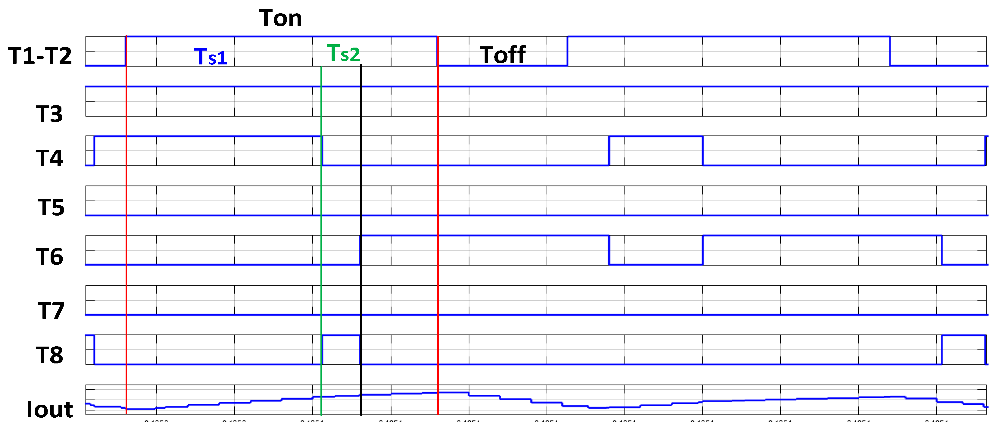
The two states ON/OFF of the V-I have a time duration Ton and Toff, in which several commutations occur in the CSI converter. The current of the CSI was short-circuited when two transistors of one leg were switched at the same time (T3 and T4 in Ts1). In Ts2, two transistors were closed in the upper and lower aspects of different branches (T3 and T8), and the current flowed through the load connected to the CSI. This occurred as long as transistors of V-I and T1–T2 were turned on (Ton). In time, Ts3, the conduction of the current, continued, but now it passed through T3, which was in the upper part of the branch, and through T6, which belonged to the lower part of the leg 2, and also through the load that of CSI. These sequences were repeated, whereas the V-I converter was in the ON state. If the transistors were open, the current descended and presented a slope of fall for the duration of Toff, as shown in Figure 12.
Under modulation conditions of B, the frequency of V-I was double that of CSI, and the current of CSI was again short-circuited, when two transistors of one leg were switched at the same time (Ts1), the current having a slope positive. In the next period Ts2, the current flowed by transistors of two different legs (T3–T8), and closed for the load that was connected to CSI, then having a positive ramp but a lower slope. This happened as long as the transistors of V-I TA–TB were turned on (Ton) (Figure 13).
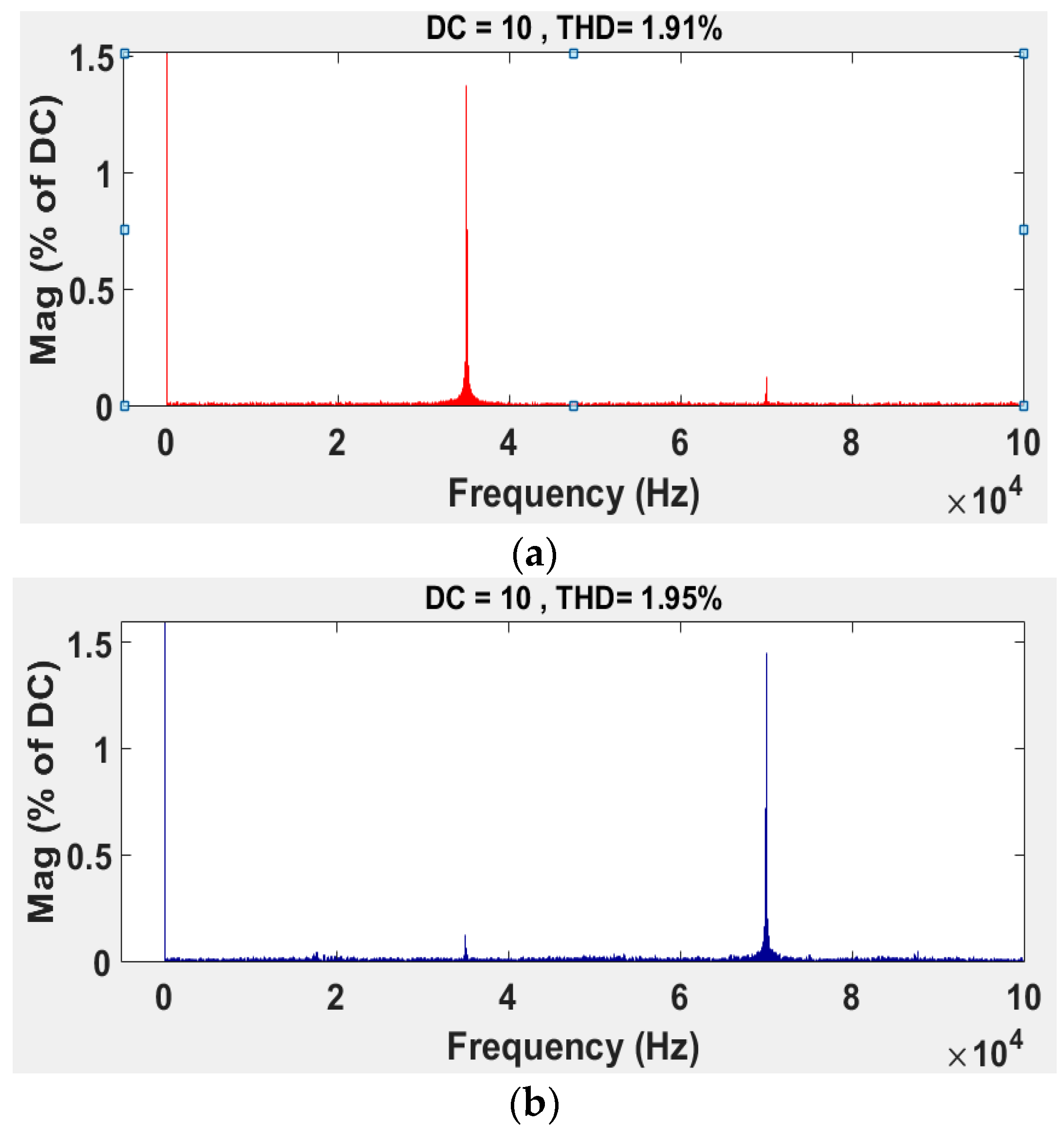
These two cases were compared, and the THD of the V-I output current was analyzed with a DC component. The results obtained were shown in Figure 14. As shown, somewhat less distortion with a higher harmonic order appeared in case B, i.e., the CSI switching frequency was double the V-I one.
The next step was to develop an analysis that consisted of moving the angle-shift for the carrier signals of the converters. The displacement was a range of 0° to 180° in steps of 30 grades. After that, performing a calculation of THD for each set point of phase-shift with the previously selected frequency values regarding the result shown in Figure 15, the THD was reduced to 1.98% when the shifting between the carrier signals was 90°.
To understand the THD related to the phase change between carrier signals, the CSI and V-I activation signal map was analyzed. Also, the conduction and short-circuit sequence were established for each instant of turning ON and OFF the V-I converter. For the situation of 0° degrees of phase shift, the signal activation map of CSI and V-I is shown in Figure 16.
Where C is the situation of conduction, and * is the situation of the short circuit. The sequence for this situation is C*CC*CC|C*CC*CC, and it is repeated for all cycles. The signals map for the phase angles of 90° and 120° are shown in Figure 17; in these situations, the highest and lowest value of THD is produced.
In the first situation, (a) it was observed that there were two short-circuit states with short durations when the V-I converter was in the OFF state, and two short-circuits with a short times of duration in the ON state. In (b) situation, it was observed that there were three short-circuit states for each ON and OFF state of the V-I. From this analysis, it can be concluded that the more short-circuit states a with minor time of duration in the CSI, the higher a THD is generated, and when there are less short-circuit states with minor times, a reduction in the THD is obtained. Finally, the duration time of the short-circuit also increments the THD for the same number of short-circuit states. Table 3 shows the result of THD for each situation of angle shift and sequence of the conduction–short circuit that is obtained.
The output currents and the THD analysis for the condition of fsvi = 35 kHz and fscsi = 70 kHz with an offset angle between the signals carriers of 90° are shown in Figure 18.
In addition, the same analysis was realized but now with the V-I frequency ratio of 70 kHz, the CSI at 35 kHz and shift-angles of 0°, 90° and 120°. The results are shown in Figure 19.
The results of these switching patterns indicate that if the frequency of the V-I is double that of the CSI, the short-circuit the time increase. This produces a greater harmonic distortion in the output currents. The THD obtained in these three phase situations are shown in Table 4.
In this way it was determined that situation B is the most optimal, and when the shift angle between the carriers is 90° in this condition, the smallest THD value of the whole analysis is obtained.
4. Analysis of Power Losses, Temperature and Efficiency
4.1. Power Losses and Efficiency in the V-I Power Converter
The power losses analyzed were the conduction and switching losses. The parameters of device SiC are shown in Table 5.
The conduction losses in the MOSFET SiC and diode SiC could be expressed for (9) and (10); the switching losses in the Mosfet SiC and SiC diode were expressed in (11) and (12) [4,5,6,7,8,9,10,11,12,13,14,15,16,17,18,19,20,21,22,23,24]:
where Rds is the drain-source resistor of SiC MOSFET, Irms were the effective current flowing in the device. IDc is the value of the current flowing through the diode, respectively:
where EON is the turn-on switching energy, EOFF is the turn-off switching energy in the MOSFET SiC and EswD is the energy of switching in the SiC Schottky diode [18]. The Eon, Eoff, and EswD are calculated by (13)–(15):
where VDS is the voltage drain source, ID the continuous drain current, Vdc is the voltage Dc link; the tri, tfv, and Qrr are the current rise time, voltage fall time, and the reverse recovery charge, respectively [24]. All these parameters are in the datasheet of the devices.
4.2. Inductor Core Losses
The losses in the inductors are from the following sources, hysteresis loss, copper or winding loss and eddy current loss. The hysteresis loss is due to the materials intrinsic properties, due to the energy used to align and re-align the magnetic domains. The general form of the losses for hysteresis Pm is calculated by the Expression (16):
where a, d, and k are constants, depending of the type of material, for this case is ferrite. Eddy current loss from the circulating currents within the magnetic materials, due to the differential in flux voltage inside the cores itself [25]. These losses were highly dependent upon the thickness of the walls of the cores. The eddy current loss per unit of volume could be calculated by Expression (17):
where η is the Steinmetz hysteresis constant, and ρ is the density of the material. The copper losses in the inductor are calculated by Expression (18):
The total power losses in the inductor are obtained by the Expression (19) and are shown in Table 6:
The rated power of the V-I converter is 1 kW. Figure 20 shows the analysis of power losses and efficiency in the V-I power converter switching at 35 kHz, with a phase-shift of 90° in PWM carriers. Efficiency is calculated with Expression (20):
4.3. Power Losses and Efficiency in the Current Source Inverter
In the case of the CSI converter, the important rule for the calculation of losses is that there is at least one device turned on in the converter [24]. The expressions that were implemented to calculate the losses for switching and conduction were as in the previous section. However, this time the topology of a Schottky SiC diode connected in series with each SiC MOSFET was considered. The results of power losses in the CSI converter by switching and conduction to 70 kHz, and 90° of phase shift in the PWM carriers are presented in Figure 21. The rated power of the CSI converter was 1.5 kW.
4.4. Power Losses in the Electric Motor
This section presents the analysis of the power losses in the electric motor, considering four situations of operation previously analyzed, 0 degrees, 60 degrees, 90 degrees (angle with lower THD), 120 degrees of phase shift in PWM carriers for V-I and CSI converters. This analysis aims to perform a comparative study and to show that the reduction of harmonics allows for the improvement of the efficiency of the electric motor.
In the permanent magnet synchronous motor (PMSM), there are two main electrical losses, the core losses in the iron core, and the copper losses in the winding. The fundamental iron loss consisted of hysteresis loss and eddy current loss, and copper losses, which were caused by the stator coil resistance Rs [26,27]. The copper losses were the losses due to the heat (Joule effect) that produced the current when it was circulated by a conductor, and it could be expressed by (21). In the analysis, the data of a PMSM engine implemented in another previous study was considered [27,28].
where m is the number of phases, Rs is the resistance, and I is the DC current, In is the root mean square (RMS) of the nth current harmonic. Rn,ac is the value of the ohmic for the nth harmonic that is determined by Expression (22).
where Knse is the resistance gain cause for the effect skin, and Kn,pe is the resistance gain caused by the proximity effect. The iron losses are calculated on the basis of Expression (23):
where k is the coefficient of additional losses in iron, PFEo, for magnetic sheet M250-50A, fo is the frequency, Bo is the maximum induction value, Bd is the maximum induction in the teeth, Bce is the maximum induction in the stator crown, Md is mass of the teeth, and Mce is the mass of the stator crown. The result of power losses in the PMSM for the four situations are showed in Figure 22.
The representation of the efficiency of the motor for the situations of shift phase angles (0°, 60°, 90°, and 120°) are shown in Figure 23 are compared for different power outputs.
The weighted average efficiency of the whole system (power converters + motor) in the situations of 0° and 90° is shown in Table 7 and Figure 24. The study allows for the demonstration that by using the proposed method, an improvement in the efficiency of the systems analyzed is obtained.
Application of the proposed modulation patterns produced a gain in efficiency that was not highly significant (0.91%), but it was good enough to reduce the thermal stress of the power converters, the thermal behavior of the whole system, as well as the improvement of the wave shape of motor currents.
Finally, a comparative study was carried out with a hybrid DC–DC converter and VSI topology with silicon IGBTs and SiC diodes. This was done for the purpose of comparing and validating the efficiency between these topologies with frequency of operation of 5 kHz for DC–DC, and 10 kHz for VSI. The features of devices used for the hybrid DC–DC and VSI topologies are presented in Table 8.
The comparison between the two topologies in terms of power losses are shown in Table 9 and Figure 25.
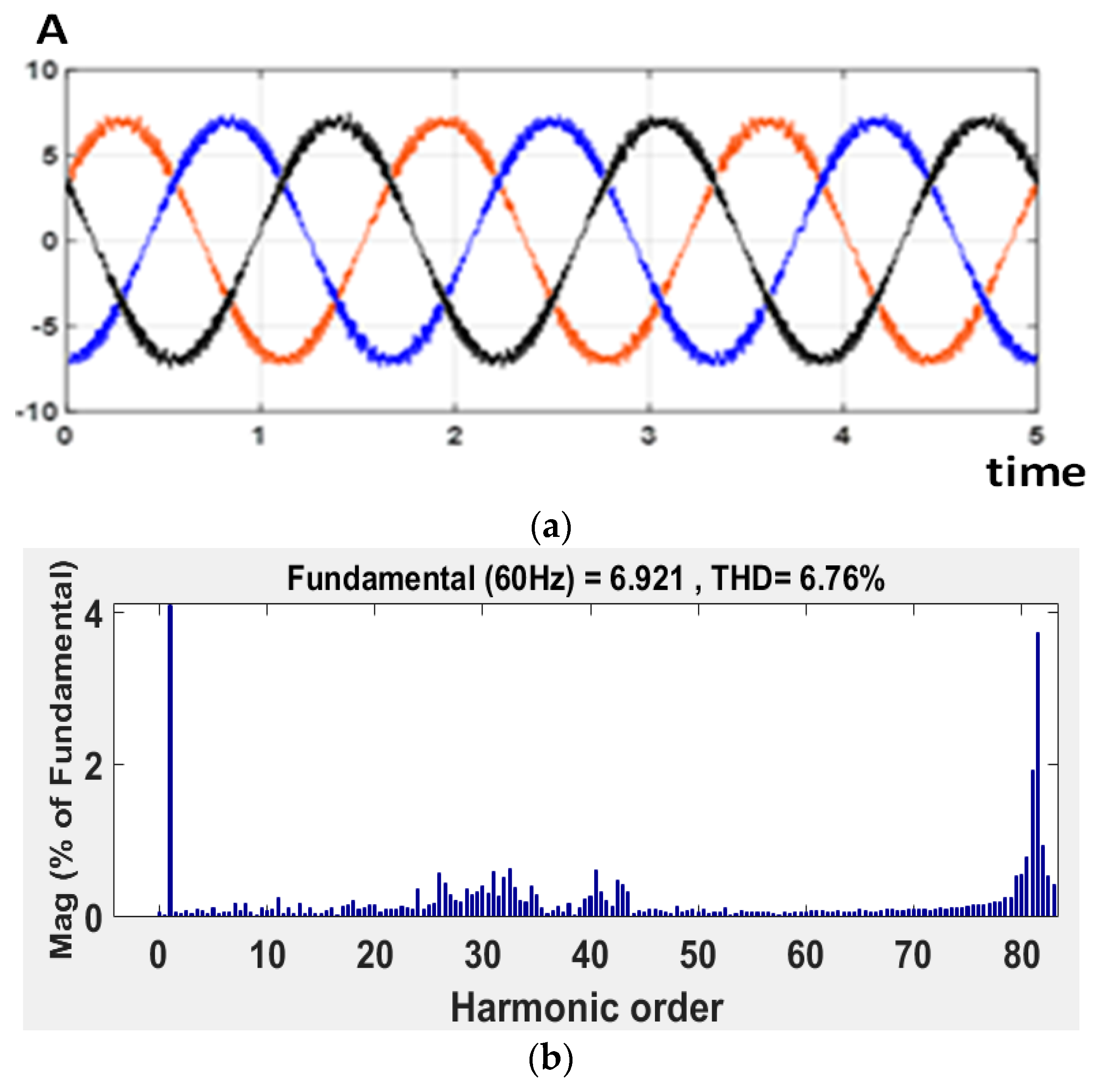
When obtaining the THD of the currents of the VSI topology (Figure 26) and comparing it with the previous analysis, it can be seen that the harmonic distortion increases to 2.52%. This causes losses throughout the system to increase.
These results justify us that the V-I topology with the CSI inverter of SiC devices presents better responses in losses and in harmonic distortion, with respect to the proposed VSI topology for the comparison.
4.5. Heatsink Estimation
The use of a cooling system or heat sink is important for the operation of converter topologies. Using a simple thermal model for SiC devices, containing a junction and a case before the heatsink, and assuming that all devices are placed on the same plate, a maximum thermal resistance for the heatsink can be estimated following the method described in [29]. The maximum allowable thermal resistance for the heatsink is calculated for Expression (24):
where the Rthhs is the heatsink temperature, Ta is the ambient temperature, and Pd is the power dissipated by the component. Applying this method gives a heatsink estimate of the heatsink of 0.68 °C/W for the V-I converter, and 0.22 °C/W for the CSI inverter, with an operating temperature of 142 °C and 25 °C of the ambient temperature.
5. Conclusions
This paper presents a method for reducing the total harmonic distortion in the output currents of a CSI topology, with a V-I power converter based on SiC. The method consists of adjusting the switching frequency and the phase-shift angle between two carrier signals. The method proposed shows positive results that allow accurate synchronization between converter topologies. Among the results obtained, it is observed that the frequency of operation of the CSI has to be higher (double), that of the V-I, to obtain a reduction of the THD.
In addition, an improvement in the efficiency is observed by varying the phase angle between PWM carriers of both power converters switching modulators, V-I and CSI. According to the comparative analysis, the results show that the efficiency increases from 91.08% to 92% by changing the phase angle from 0° to 90° of shift angle.
Finally, as a general conclusion, the use of SiC devices in the topologies of inverters with current sources (CSI) allows for an increase in the frequency of switching, and improvements in their efficiency. This efficiency could even be increased by a proper adjustment of switching frequencies. These advantages could translate into a substantial reduction of inverter cost and volume, higher reliability, greater power, and improved engine efficiency, allowing for the consolidation of these topologies in electric traction systems.
Author Contributions
E.F. performed the design of method and validation in simulations. A.P. performed and assisted with the power losses and state-of-the-art methods. V.S. and L.R. contributed to objective definitions and the revision of the paper’s methodology and conclusions. All authors carried out the theoretical analysis and contributed to writing the paper.
Funding
This research received no external funding
Acknowledgments
This work was supported in part by the Spanish Ministry of Economy and Competitiveness under the TRA2016-80472-R Research Project.
Conflicts of Interest
The authors declare no conflict of interest.
References
- Bindra, A. Wide-Bandgap Power Devices: Adoption Gathers Momentum. IEEE Power Electr. Mag. 2018, 5, 22–27. [Google Scholar] [CrossRef]
- Choi, H. Overview of silicon carbide power devices. Fairchild Semicond. 2016, I, 1–6. [Google Scholar]
- She, X.; Huang, A.Q.; Lucía, Ó.; Ozpineci, B. Review of silicon carbide power devices and their applications. IEEE Trans. Ind. Electr. 2017, 64, 8193–8205. [Google Scholar] [CrossRef]
- Shang, F.; Arribas, A.P.; Krishnamurthy, M. A comprehensive evaluation of SiC devices in traction applications. In Proceedings of the 2014 IEEE Transportation Electrification Conference and Expo (ITEC), Dearborn, MI, USA, 15–18 June 2014; pp. 1–5. [Google Scholar]
- Merkert, A.; Müller, J.; Mertens, A. Component design and implementation of a 60 kW full SiC traction inverter with boost converter. In Proceedings of the Energy Conversion Congress and Exposition (ECCE), Milwaukee, WI, USA, 18–22 September 2016; pp. 1–8. [Google Scholar]
- Attia, Y.; Abdelrahman, A.; Hamouda, M.; Youssef, M. SiC devices performance overview in EV DC/DC converter: A case study in a Nissan Leaf. In Proceedings of the 2016 IEEE Transportation Electrification Conference and Expo, Asia-Pacific (ITEC Asia-Pacific), Busan, Korea, 1–4 June 2016; pp. 214–219. [Google Scholar]
- Han, D.; Li, S.; Wu, Y.; Choi, W.; Sarlioglu, B. Comparative analysis on conducted CM EMI emission of motor drives: WBG versus Si devices. IEEE Trans. Ind. Electr. 2017, 64, 8353–8363. [Google Scholar] [CrossRef]
- Ding, X.; Cheng, J.; Chen, F. Impact of silicon carbide devices on the powertrain systems in electric vehicles. Energies 2017, 10, 533. [Google Scholar] [CrossRef]
- Abdelrahman, A.S.; Erdem, Z.; Attia, Y.; Youssef, M.Z. Wide Bandgap Devices in Electric Vehicle Converters: A Performance Survey. Can. J. Electr. Comput. Eng. 2018, 41, 45–54. [Google Scholar]
- Ozpineci, B.; Tolbert, L.M.; Islam, S.K.; Theiss, T.J. A parametric device study for SiC diodes in vehicular applications. IEEE Veh. Technol. Conf. 1999, 3, 1495–1499. [Google Scholar]
- Han, D.; Li, Y.; Sarlioglu, B. Analysis of SiC based power electronic inverters for high speed machines. In Proceedings of the 2015 IEEE Applied Power Electronics Conference and Exposition (APEC), Charlotte, NC, USA, 15–19 March 2015; pp. 304–310. [Google Scholar]
- Han, D.; Noppakunkajorn, J.; Sarlioglu, B. Comprehensive efficiency, weight, and volume comparison of SiC-and Si-based bidirectional DC–DC converters for hybrid electric vehicles. IEEE Trans. Veh. Technol. 2014, 63, 3001–3010. [Google Scholar] [CrossRef]
- Sasagawa, M.; Nakamura, T.; Inoue, H.; Funaki, T. A study on the high frequency operation of DC-DC converter with SiC DMOSFET. In Proceedings of the Power Electronics Conference (IPEC), Sapporo, Japan, 21–24 June 2010; pp. 1946–1949. [Google Scholar]
- Sarigiannidis, A.G.; Kladas, A.G. Switching frequency impact on permanent magnet motors drive system for electric actuation applications. IEEE Trans. Magn. 2015, 51, 1–4. [Google Scholar] [CrossRef]
- Emadi, A.; Williamson, S.S.; Khaligh, A. Power electronics intensive solutions for advanced electric, hybrid electric, and fuel cell vehicular power systems. IEEE Trans. Power Electr. 2006, 21, 567–577. [Google Scholar] [CrossRef]
- Su, G.J.; Ning, P. Loss modeling and comparison of VSI and RB-IGBT based CSI in traction drive applications. In Proceedings of the Transportation Electrification Conference and Expo (ITEC), Detroit, MI, USA, 16–19 June 2013; pp. 1–7. [Google Scholar]
- Gnanasambandam, K.; Rathore, A.K.; Edpuganti, A.; Srinivasan, D.; Rodriguez, J. Current-Fed multilevel converters: An overview of circuit topologies, modulation techniques, and applications. IEEE Trans. Power Electr. 2017, 32, 3382–3401. [Google Scholar] [CrossRef]
- Mohammadi, M.; Moghani, J.S.; Milimonfared, J. A Novel Dual Switching Frequency Modulation for Z-Source and Quasi-Z-Source Inverters. IEEE Trans. Ind. Electr. 2018, 65, 5167–5176. [Google Scholar] [CrossRef]
- Tang, L.; Su, G.J. Boost mode test of a current-source-inverter-fed permanent magnet synchronous motor drive for automotive applications. In Proceedings of the 2010 IEEE 12th Workshop on Control and Modeling for Power Electronics (COMPEL), Boulder, CO, USA, 28–30 June 2010; pp. 1–8. [Google Scholar]
- Su, G.J.; Tang, L. Current source inverter based traction drive for EV battery charging applications. In Proceedings of the Vehicle Power and Propulsion Conference (VPPC), Chicago, IL, USA, 6–9 September 2011; pp. 1–6. [Google Scholar]
- Su, G.; Tang, L. A Current Source Inverter Based Motor Drive for EV/HEV Applications; SAE Technical Paper 2011-01-0346. 2011. Available online: https://doi.org/10.4271/2011-01-0346 (accessed on 16 October 2018).
- Abdelsalam, A.K.; Massoud, A.; Darwish, A.; Ahmed, S. Simplified generic on-line PWM technique for single phase grid connected current source inverters. In Proceedings of the 2012 Twenty-Seventh Annual IEEE Applied Power Electronics Conference and Exposition (APEC), Orlando, FL, USA, 5–9 February 2012; pp. 1398–1403. [Google Scholar]
- Masoud, M.I.; Abdel-Khalik, A.S. Vector controlled five-phase PWM-CSI induction motor drive. In Proceedings of the Power Engineering, Energy and Electrical Drives (POWERENG), Istanbul, Turkey, 13–17 May 2013; pp. 258–264. [Google Scholar]
- Bierhoff, M.H.; Fuchs, F.W. Semiconductor losses in voltage source and current source IGBT converters based on analytical derivation. In Proceedings of the Power Electronics Specialists Conference, Aachen, Germany, 20–25 June 2004; pp. 2836–2842. [Google Scholar]
- Huynh, C.; Zheng, L.; Acharya, D. Losses in High Speed Permanent Magnet Machines Used in Microturbine Applications. J. Eng. Gas Turbines Power 2008, 131, 022301. [Google Scholar] [CrossRef]
- Guo, Q.; Zhang, C.; Li, L.; Zhang, J.; Liu, J.; Wang, T. Efficiency optimization control of permanent-magnet synchronous machines for electric vehicle traction systems. In Proceedings of the Vehicle Power and Propulsion Conference (VPPC), Hangzhou, China, 17–20 October 2016; pp. 1–5. [Google Scholar]
- Hassan, W.; Wang, B. Efficiency optimization of PMSM based drive system. In Proceedings of the 2012 7th International Power Electronics and Motion Control Conference (IPEMC), Harbin, China, 2–5 June 2012; pp. 1027–1033. [Google Scholar]
- Aguilar Gamarra, H.N. Design of a Synchronous Motor with Ferrite Magnets. Bachelor’s Thesis, Universitat Politècnica de Catalunya, Barcelona, Spain, 2014. [Google Scholar]
- Antonopoulos, A.; Bangtsson, H.; Alakula, M.; Manias, S. Introducing a silicon carbide inverter for hybrid electric vehicles. In Proceedings of the Power Electronics Specialists Conference 2008 (PESC 2008), Rhodes, Greece, 15–19 June 2008; pp. 1321–1325. [Google Scholar]
Figure 1.
Topology proposed for the study.
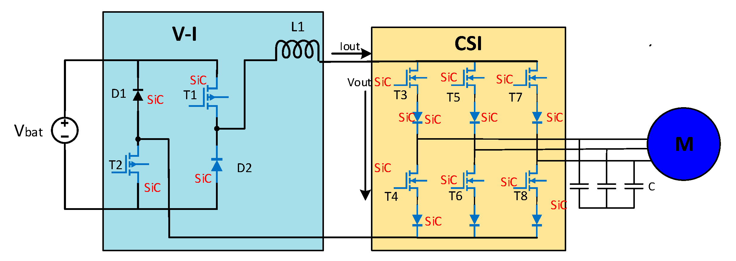
Figure 2.
Current trajectory in V-I and CSI converter V-I. (a) First state of operation; (b) second state of operation.
Figure 2.
Current trajectory in V-I and CSI converter V-I. (a) First state of operation; (b) second state of operation.
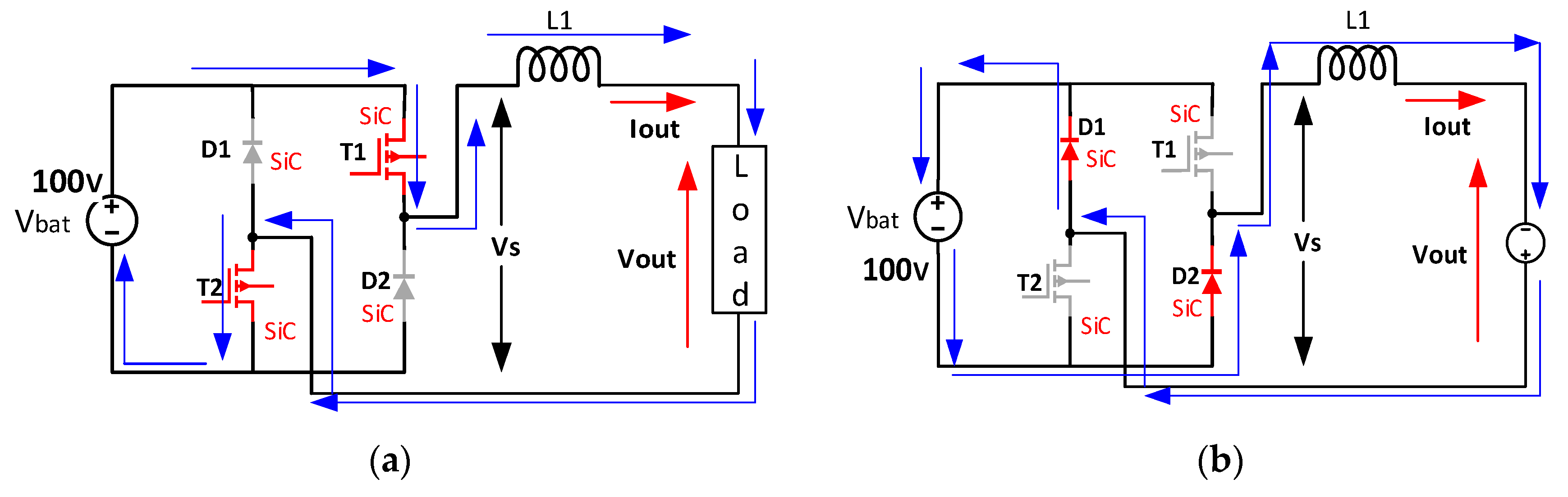
Figure 3.
Schematic of operation and synchronization of power converters.
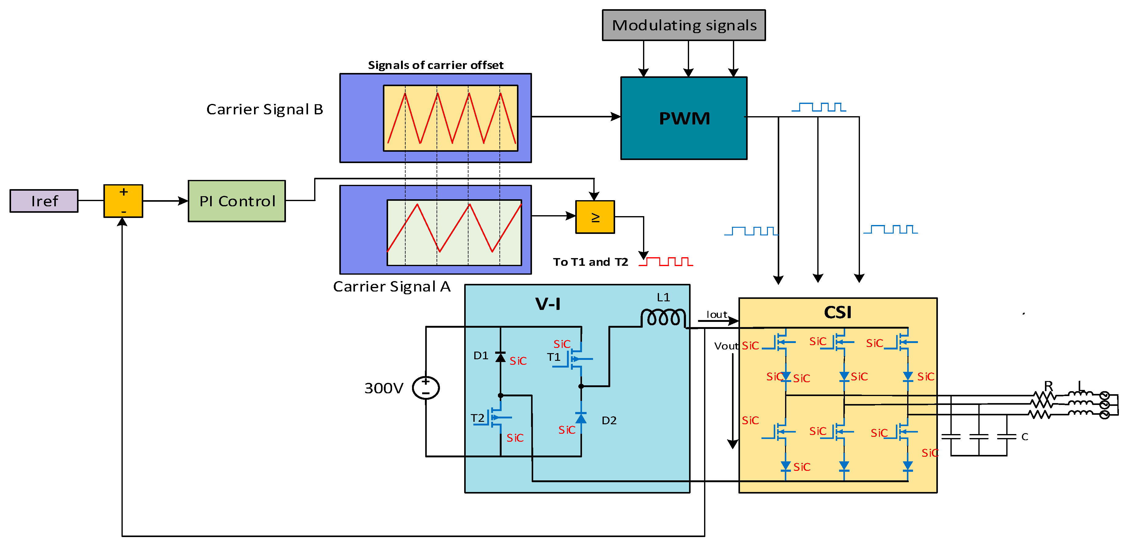
Figure 4.
V-I converter: first state of operation circuit (supplying energy).
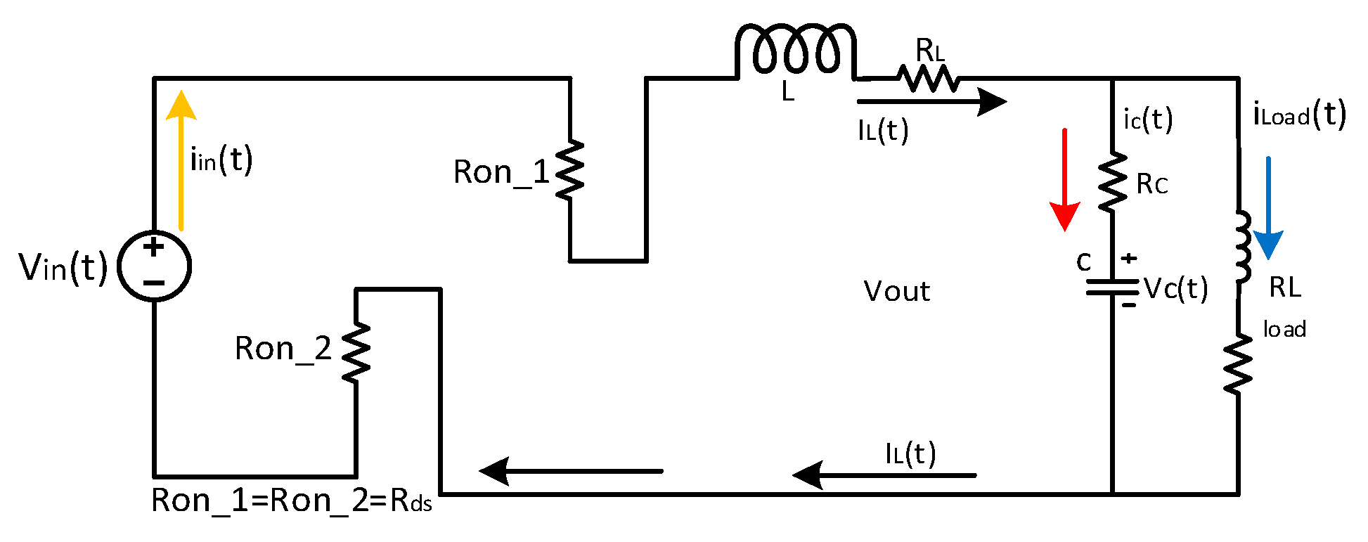
Figure 5.
Simulation results of the PI controller. (a) Output current response, (b) detail of the current reference at 10 A.
Figure 5.
Simulation results of the PI controller. (a) Output current response, (b) detail of the current reference at 10 A.
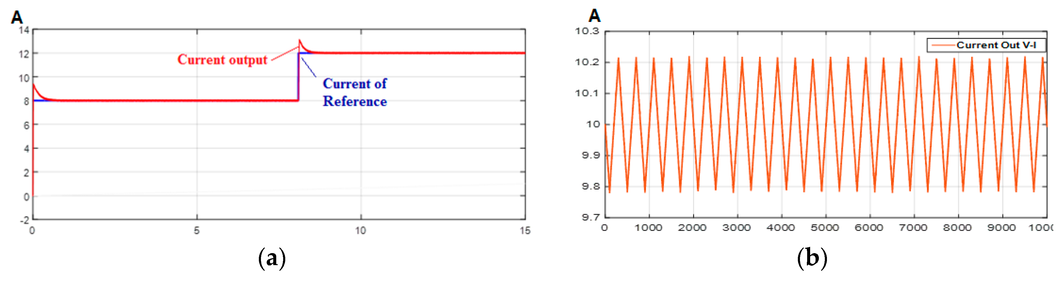
Figure 6.
Tuning of the PI controller for the V-I converter response to a step.
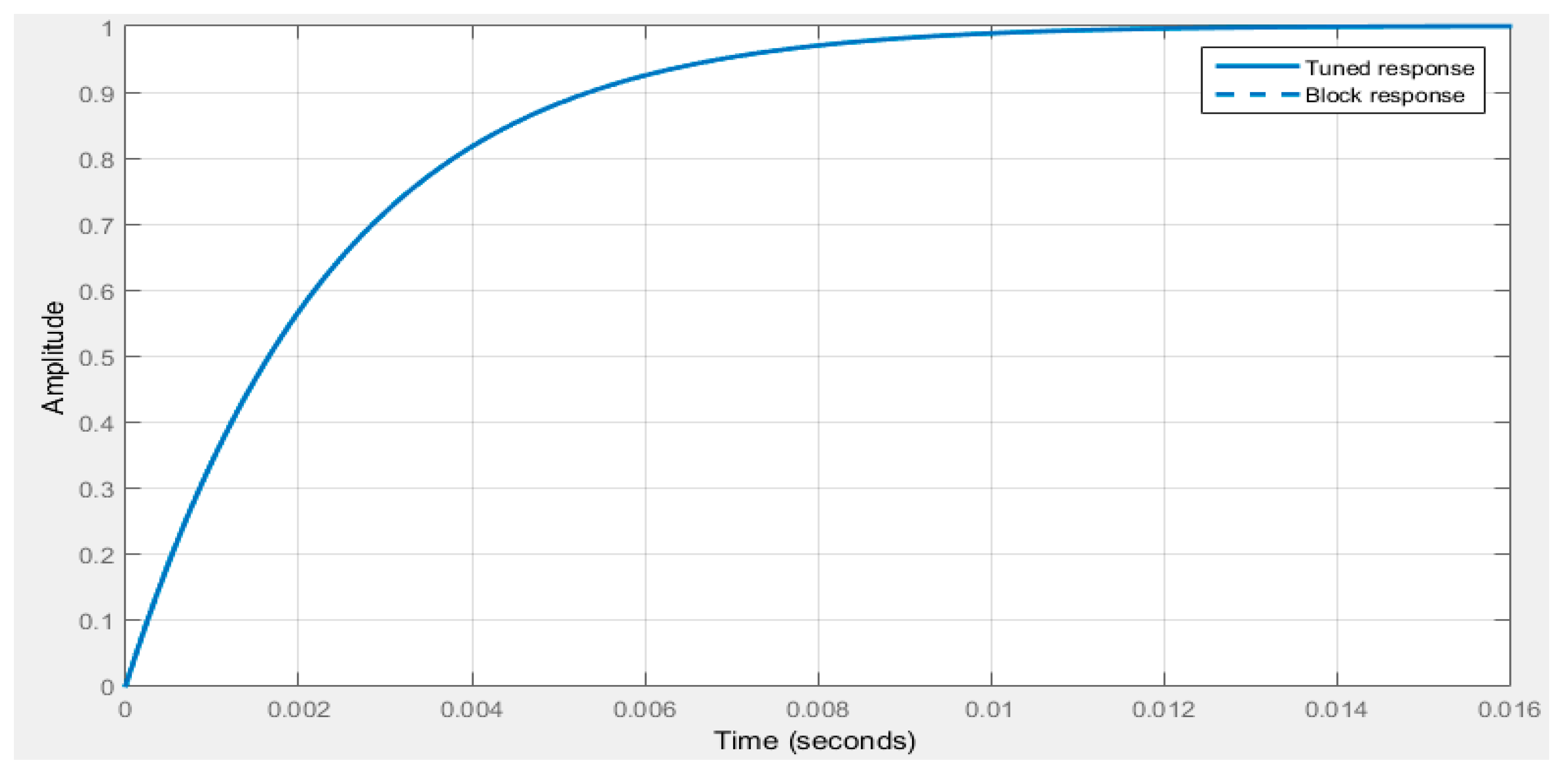
Figure 7.
Flowchart of method proposed.
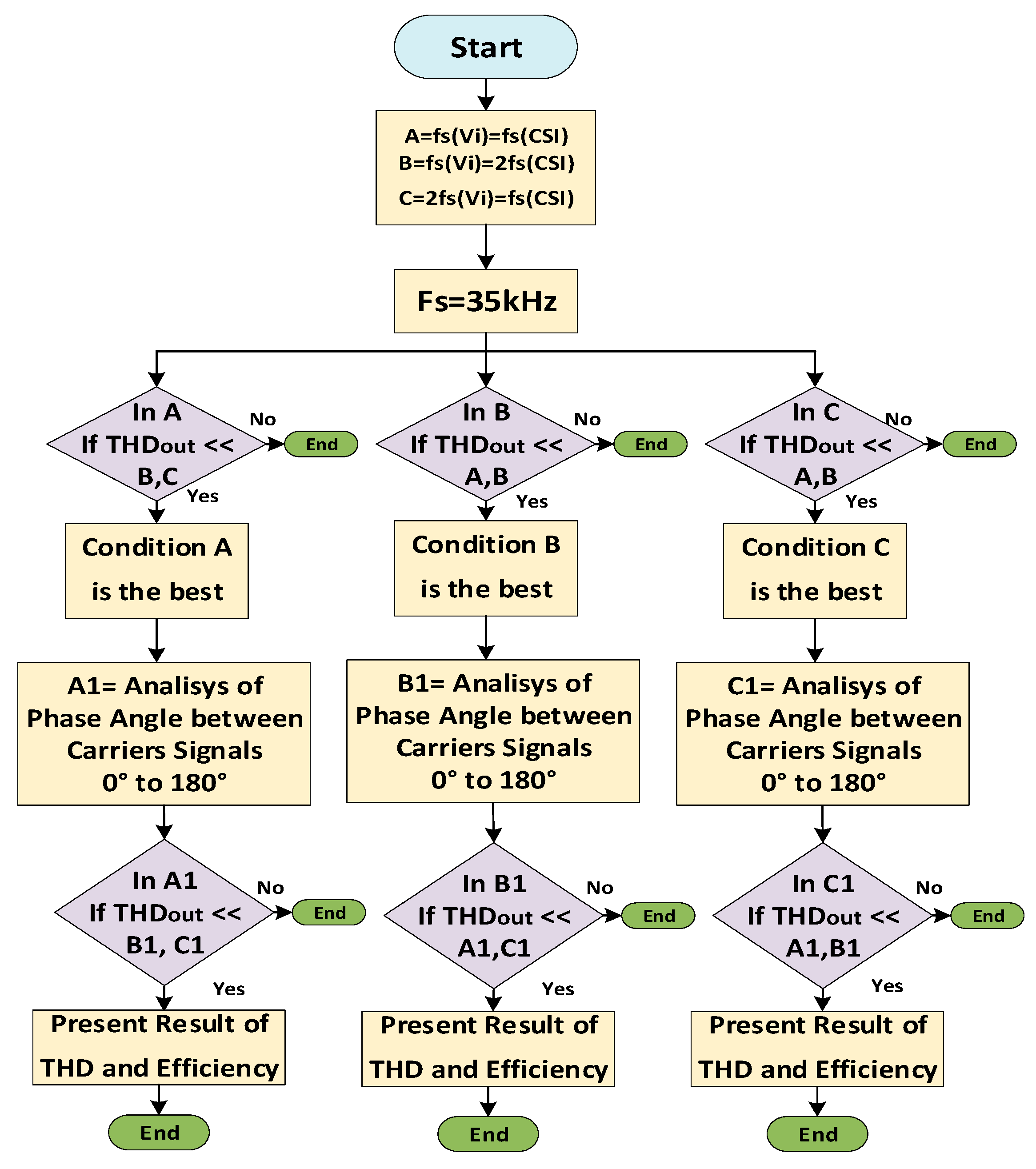
Figure 8.
Signals carriers to different frequencies and angles. (a) Fs(V-I) = 15 kHz, Fs(CSI) = 30 kHz, angle = 0°; (b) Fs(V-I) = 15 kHz, Fs(CSI) = 30 kHz angle = 90°.
Figure 8.
Signals carriers to different frequencies and angles. (a) Fs(V-I) = 15 kHz, Fs(CSI) = 30 kHz, angle = 0°; (b) Fs(V-I) = 15 kHz, Fs(CSI) = 30 kHz angle = 90°.
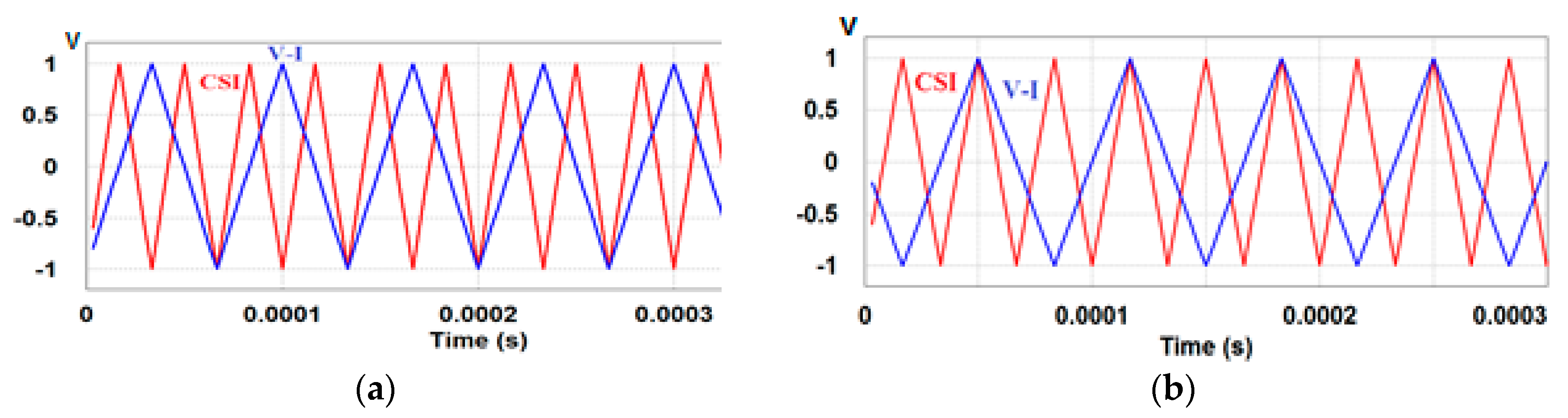
Figure 9.
Gating signal generation.
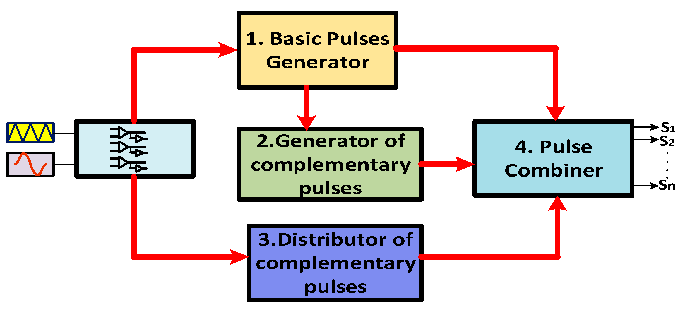
Figure 10.
Map gating signals generations. (a) Carrier and modulating signals; (b) pulse generator conventional pulse-width modulation (PWM); (c) commutation basic; (d) pulses of short circuit; (e) pulses of distribution; (f) signal of distribution; (g) signals of gating.
Figure 10.
Map gating signals generations. (a) Carrier and modulating signals; (b) pulse generator conventional pulse-width modulation (PWM); (c) commutation basic; (d) pulses of short circuit; (e) pulses of distribution; (f) signal of distribution; (g) signals of gating.
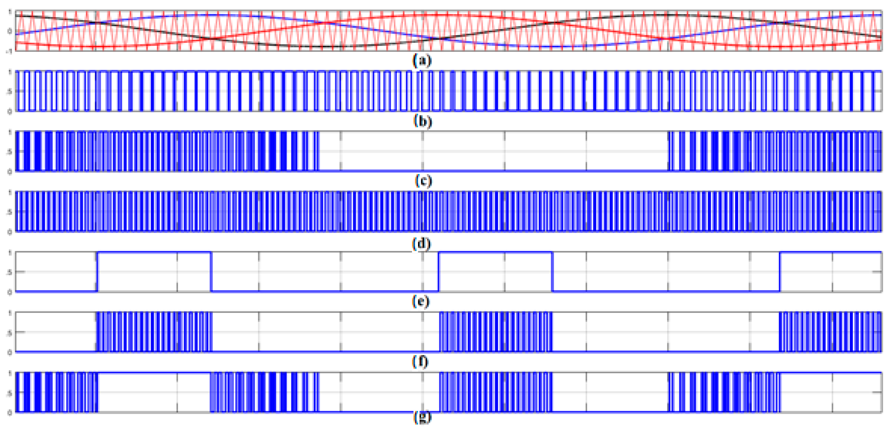
Figure 11.
Total harmonic distortion (THD) spectrum results. (a) THD spectrum for situation A, (b) THD spectrum for situation B, (c) THD spectrum for situation C, (d) comparative results graph.
Figure 11.
Total harmonic distortion (THD) spectrum results. (a) THD spectrum for situation A, (b) THD spectrum for situation B, (c) THD spectrum for situation C, (d) comparative results graph.
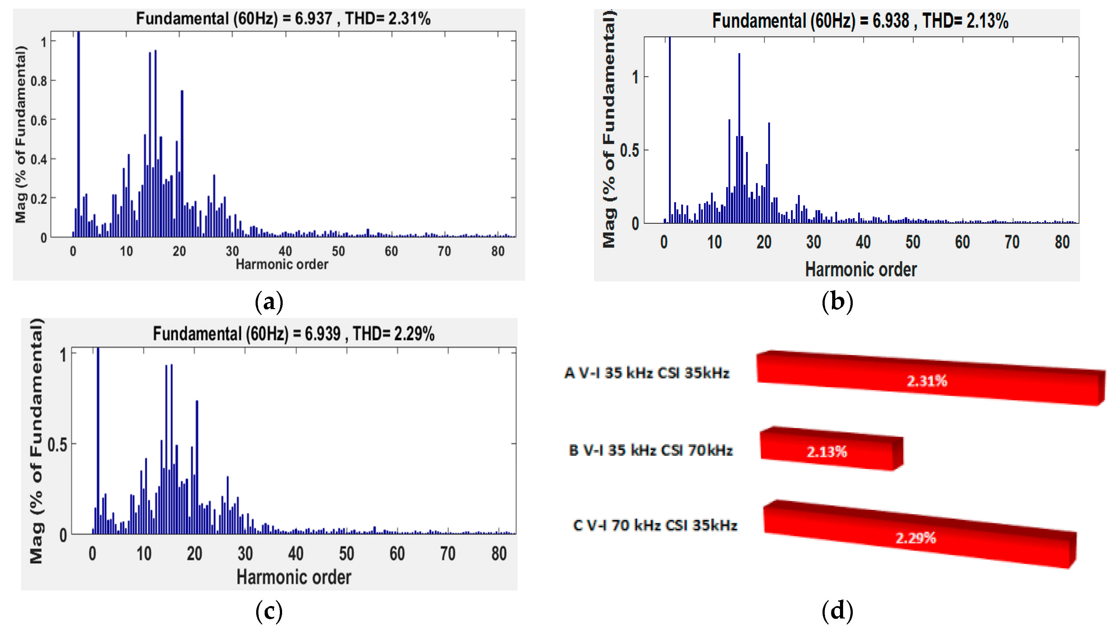
Figure 12.
Switching pattern signals for V-I–CSI to fsvi = 35 kHz and fscsi = 70 kHz.
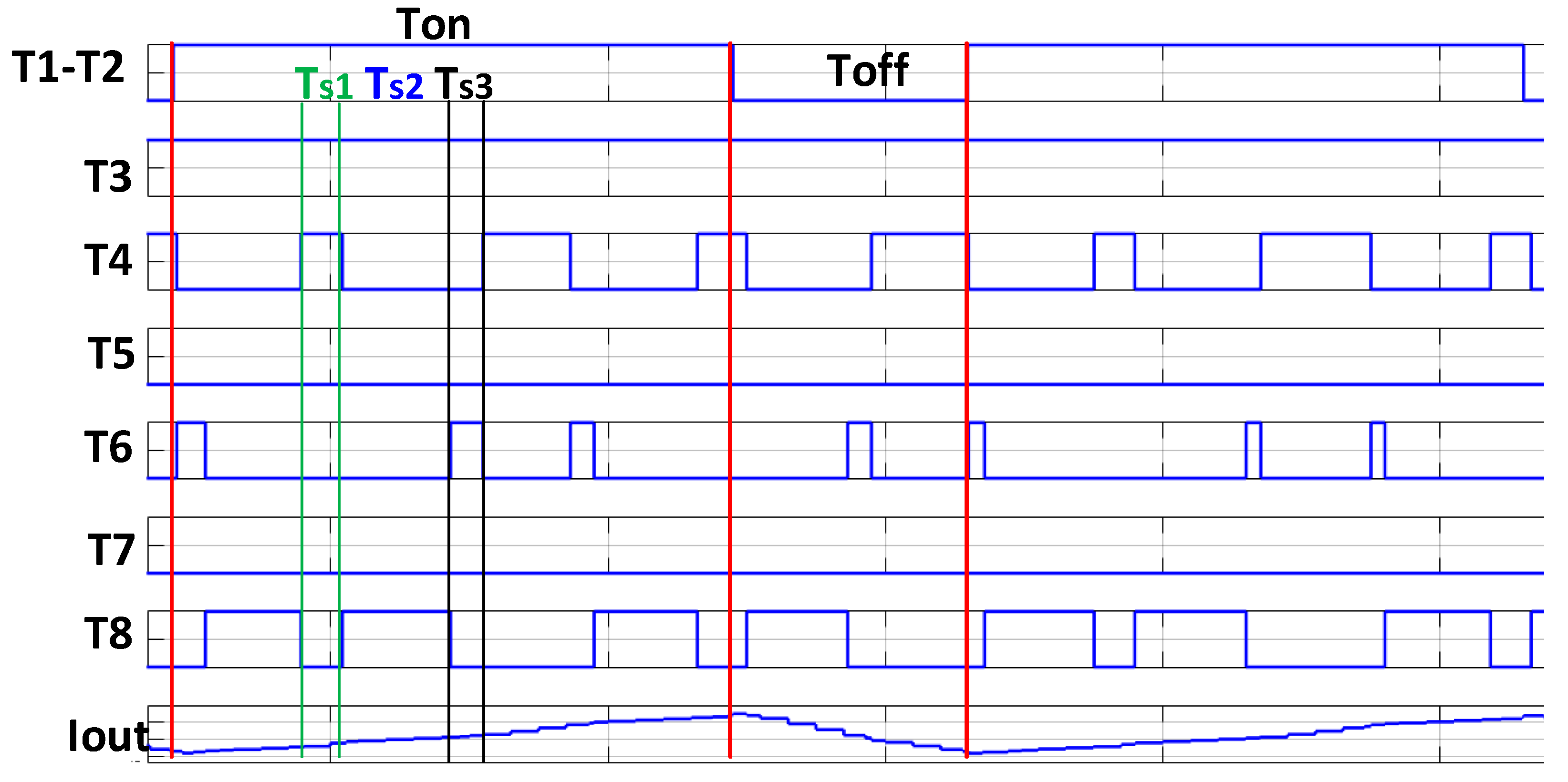
Figure 13.
Switching pattern signals in V-I-CSI to fsvi = 70 kHz and fScsi = 35 kHz.

Figure 14.
THD comparison. (a) THD in the DC output current in V-I–CSI to fsvi = 35 kHz and fscsi = 70 kHz. (b) THD in the DC output current in V-I–CSI to fsvi = 70 kHz and fscsi = 35 kHz.
Figure 14.
THD comparison. (a) THD in the DC output current in V-I–CSI to fsvi = 35 kHz and fscsi = 70 kHz. (b) THD in the DC output current in V-I–CSI to fsvi = 70 kHz and fscsi = 35 kHz.

Figure 15.
THD results for fsvi = 35 kHz and fscsi = 70 kHz when the carrier phase is sifting.
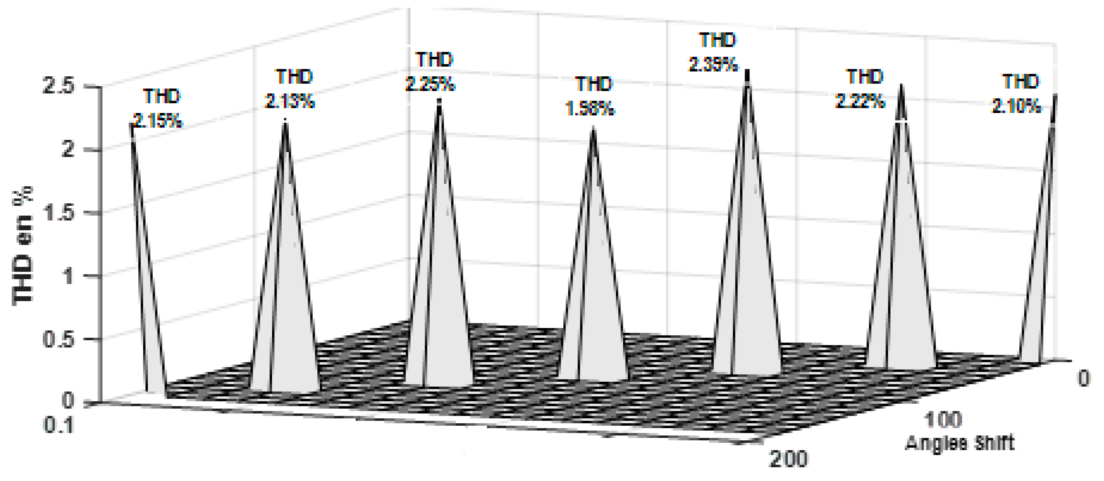
Figure 16.
Map signal in CSI and V-I with 0° of phase shift between the signal carrier.
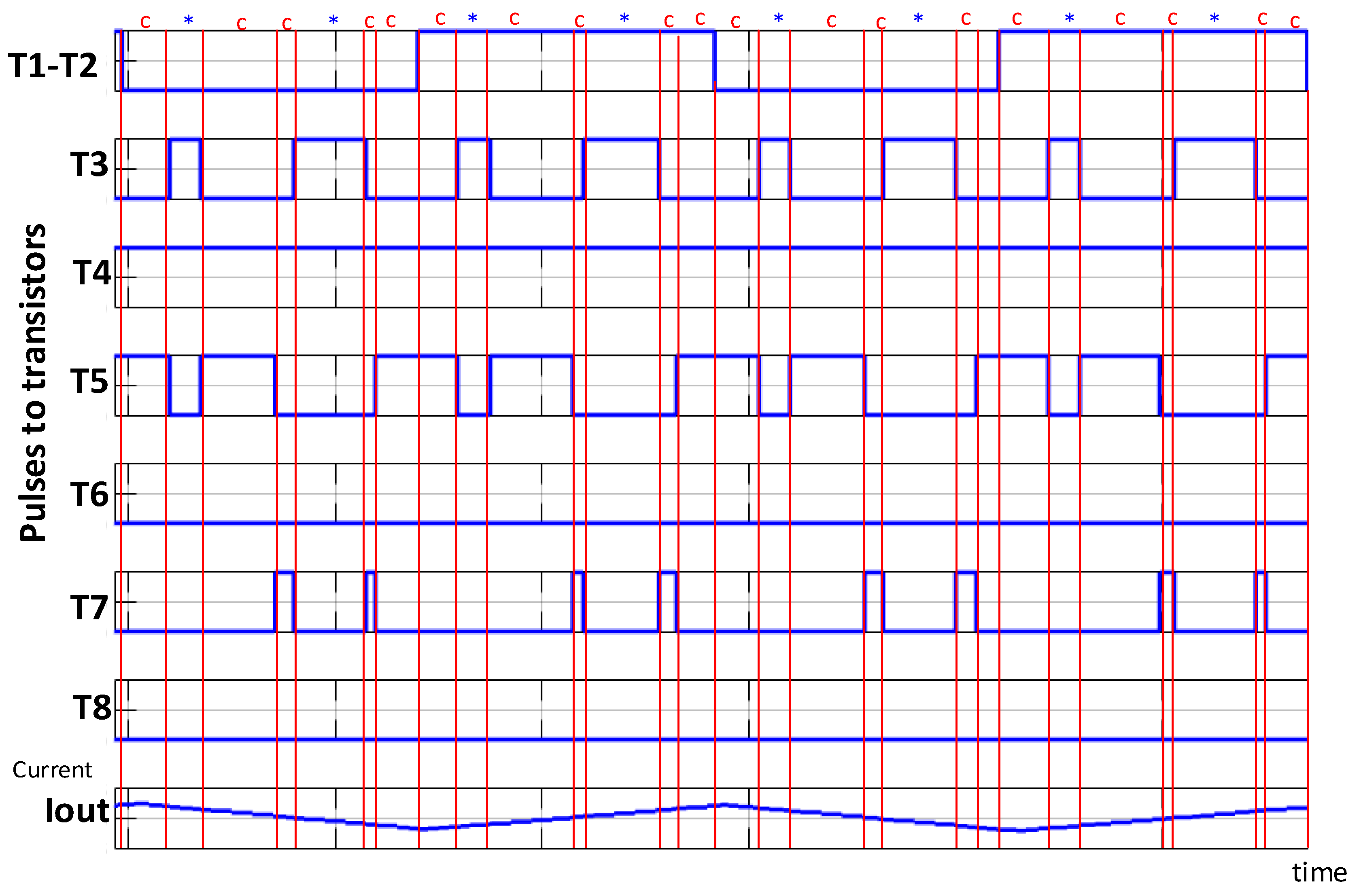
Figure 17.
Signal map in CSI and V-I: (a) Situation for 90° of phase shift, (b) situation for 120° of phase shift.
Figure 17.
Signal map in CSI and V-I: (a) Situation for 90° of phase shift, (b) situation for 120° of phase shift.
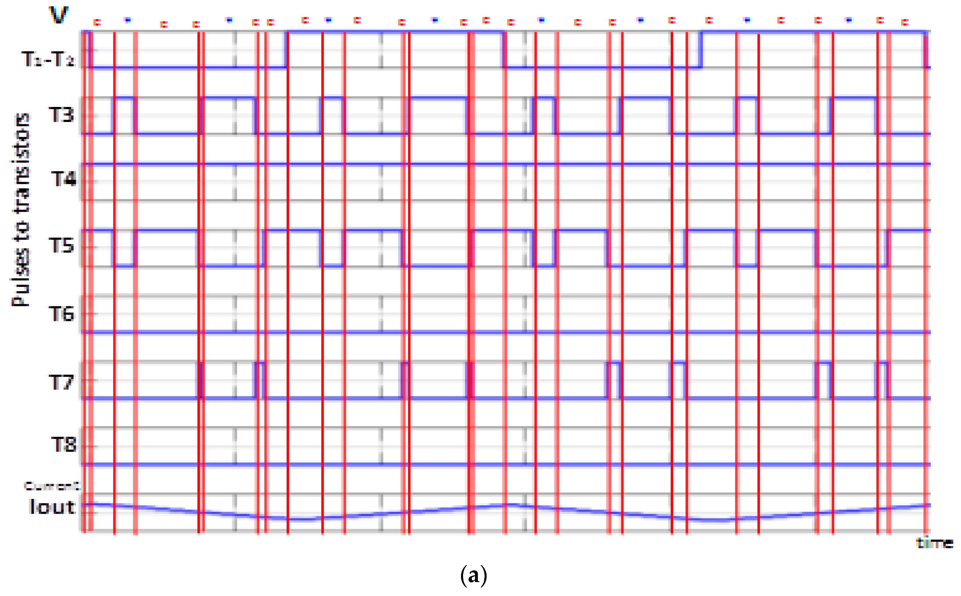
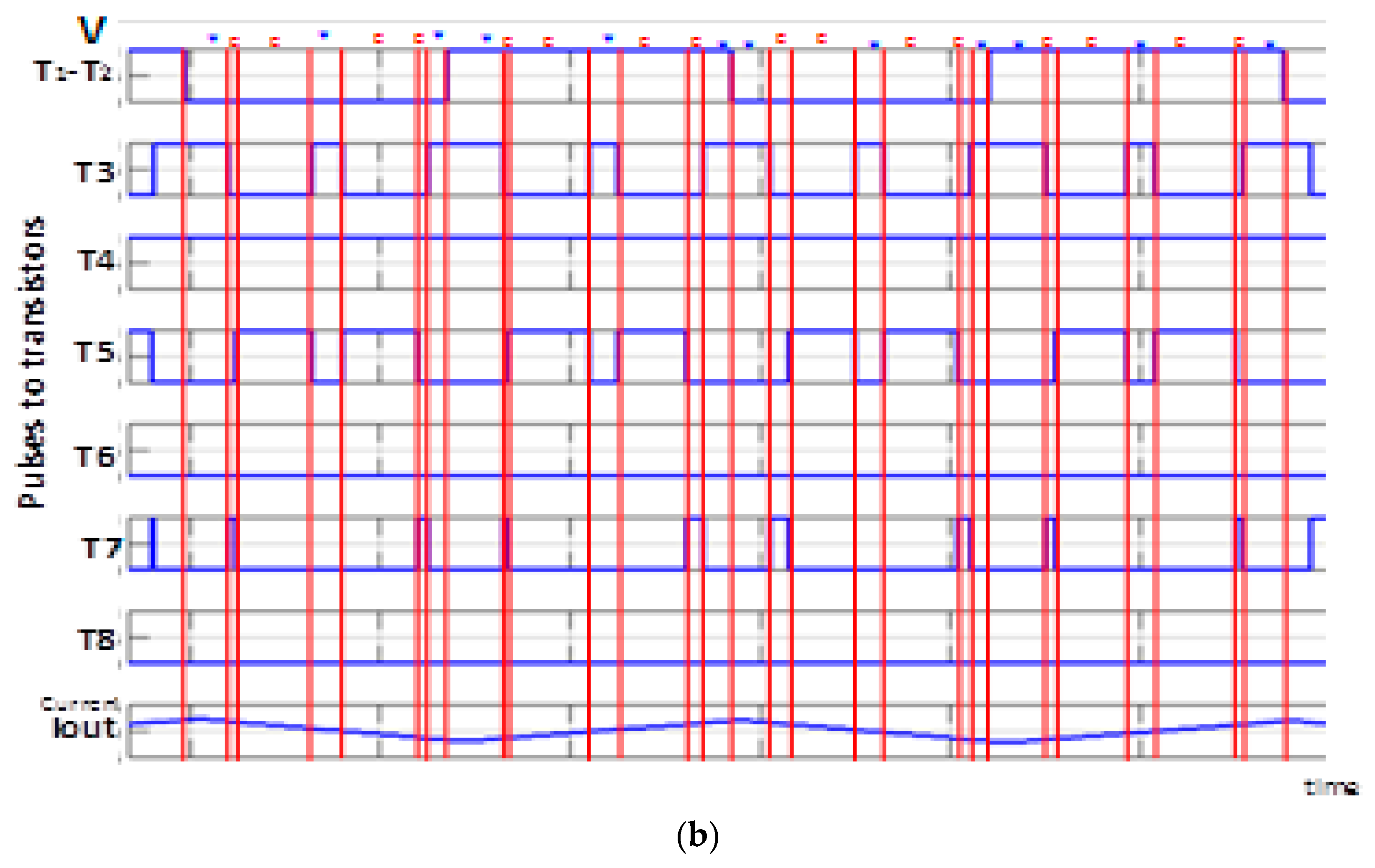
Figure 18.
Simulation results of the method for the second part: (a) currents of output in situation B and a 90° shift angle; (b) THD analysis of the output current.
Figure 18.
Simulation results of the method for the second part: (a) currents of output in situation B and a 90° shift angle; (b) THD analysis of the output current.
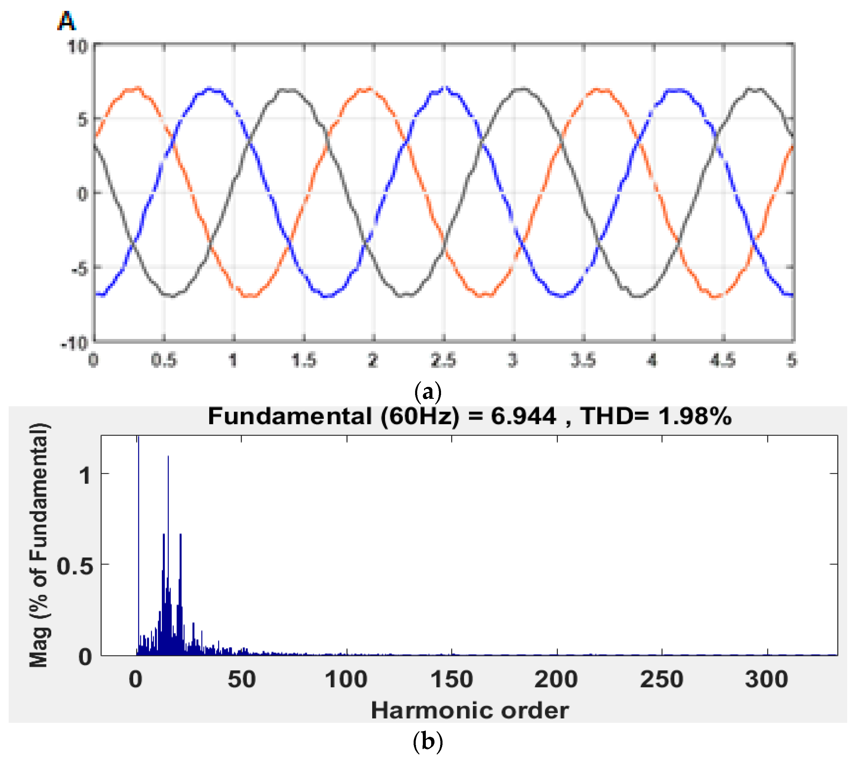
Figure 19.
Simulation results for fSV-I = 70 kHz and fscsi= 35 kHz. (a) Situation at 0° of shift angle. (b) Situation at 90° of shift angle. (c) Situation at 120° of shift-angle.
Figure 19.
Simulation results for fSV-I = 70 kHz and fscsi= 35 kHz. (a) Situation at 0° of shift angle. (b) Situation at 90° of shift angle. (c) Situation at 120° of shift-angle.
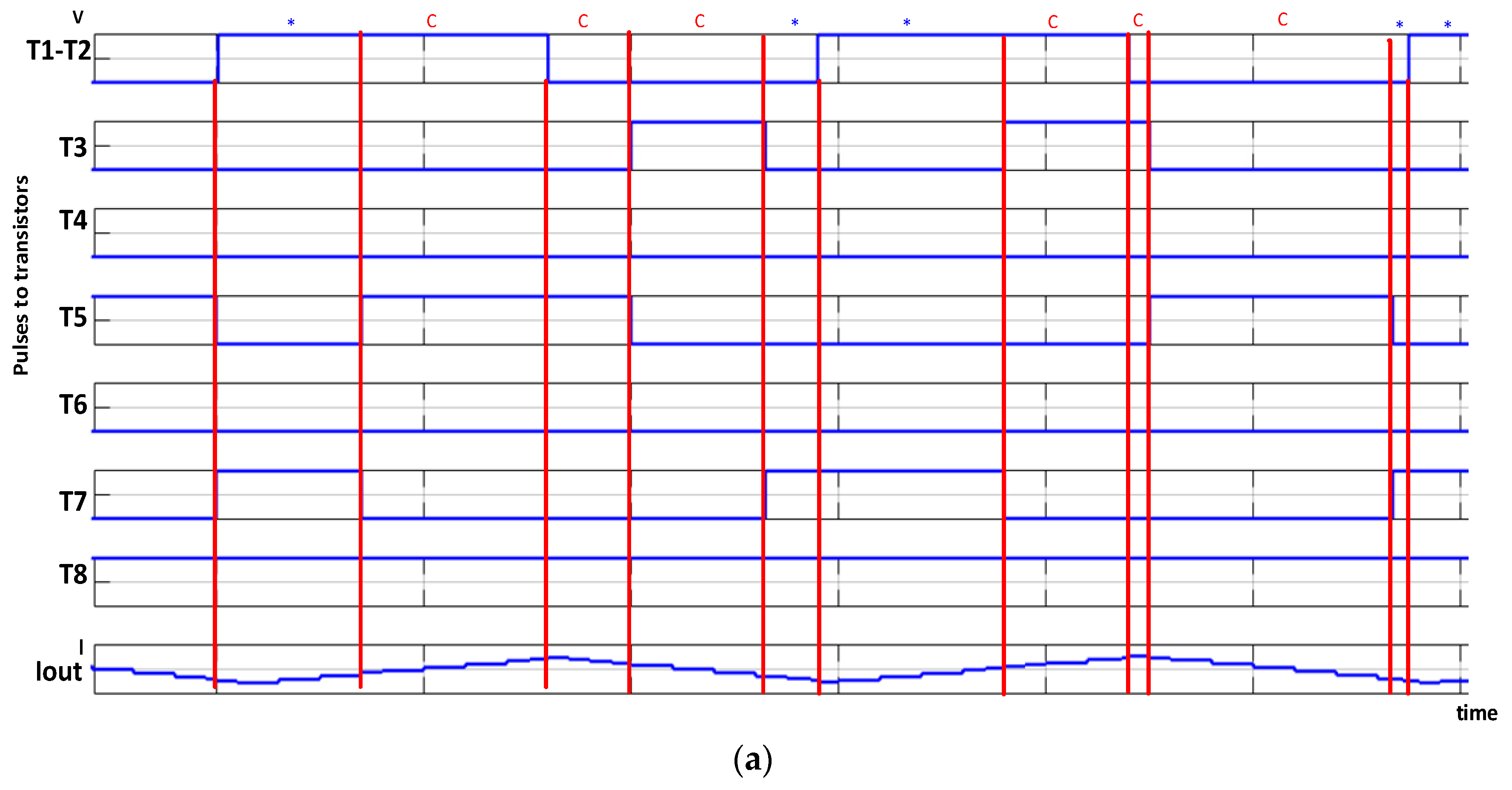
Figure 20.
Result of analysis in the V-I power converter. (a) Power losses (b) Efficiency.
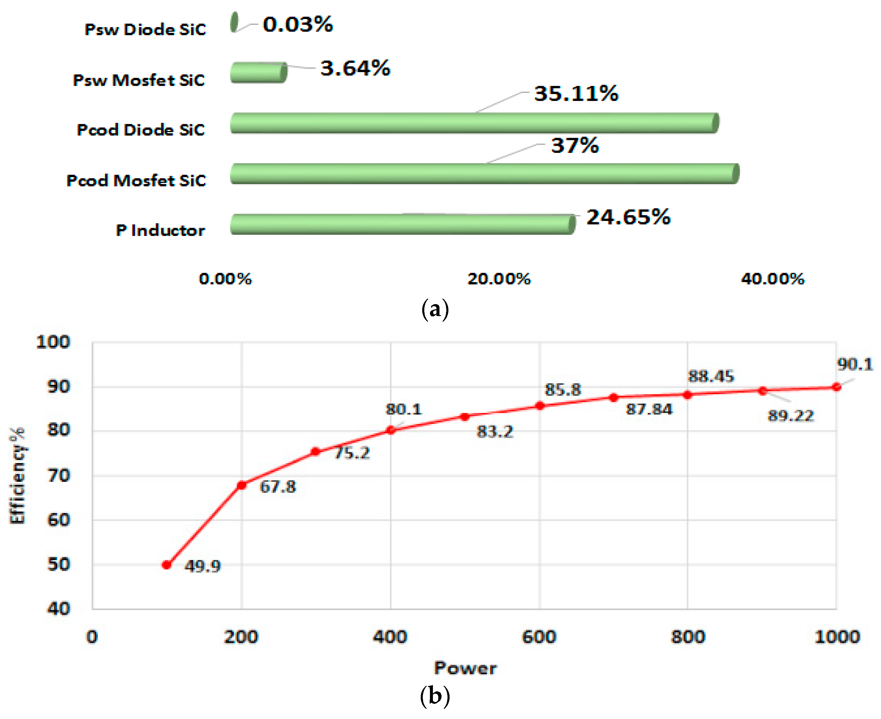
Figure 21.
Power losses and efficiency in the CSI power converter.
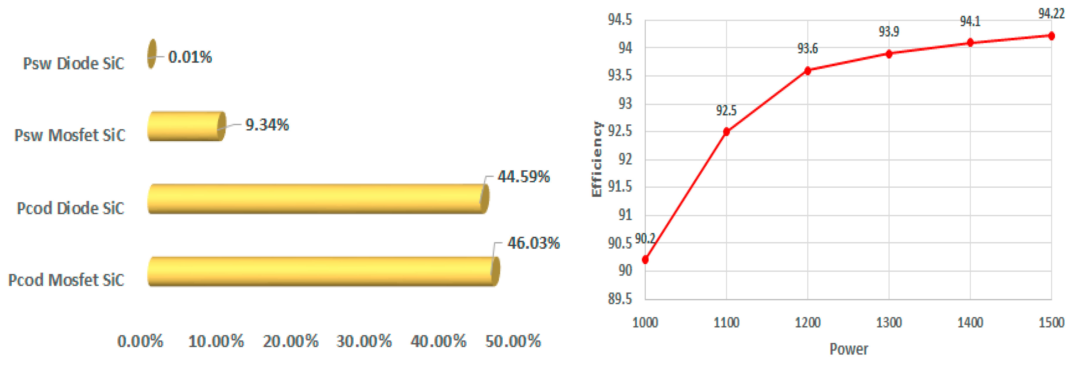
Figure 22.
Power losses in permanent magnet synchronous motor (PMSM)with shift angle in 0°, 60°, 90°, and 120° in the power converters.
Figure 22.
Power losses in permanent magnet synchronous motor (PMSM)with shift angle in 0°, 60°, 90°, and 120° in the power converters.

Figure 23.
Efficiency in an electric motor for shift angles of 0°, 60°, 90°, and 120° in the power converters.
Figure 23.
Efficiency in an electric motor for shift angles of 0°, 60°, 90°, and 120° in the power converters.
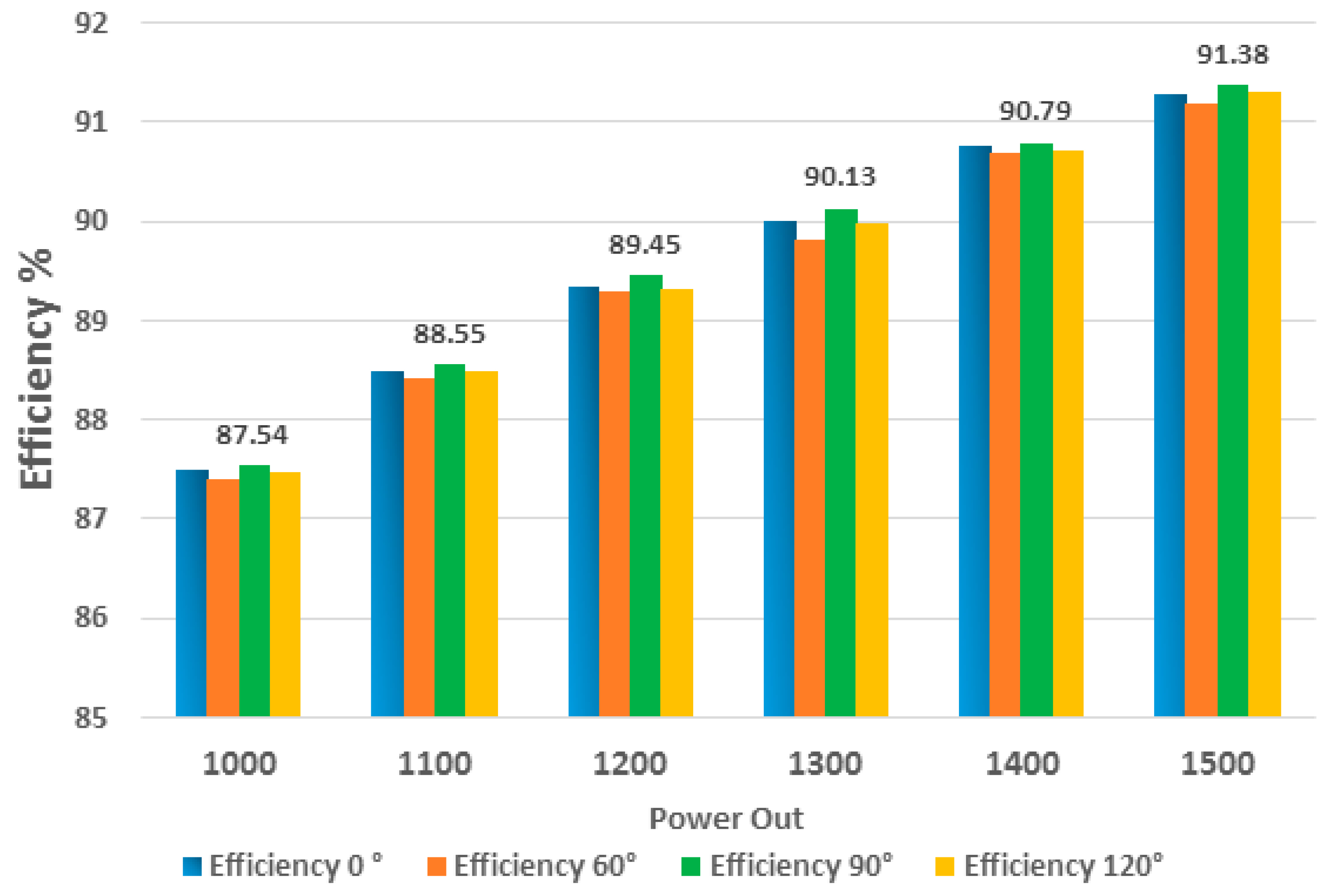
Figure 24.
Efficiency in all systems.

Figure 25.
Power losses comparison results. (a) Power losses in V-I SiC vs. DC–DC hybrid topologies. (b) Power losses in CSI SiC vs. VSI hybrid topologies.
Figure 25.
Power losses comparison results. (a) Power losses in V-I SiC vs. DC–DC hybrid topologies. (b) Power losses in CSI SiC vs. VSI hybrid topologies.
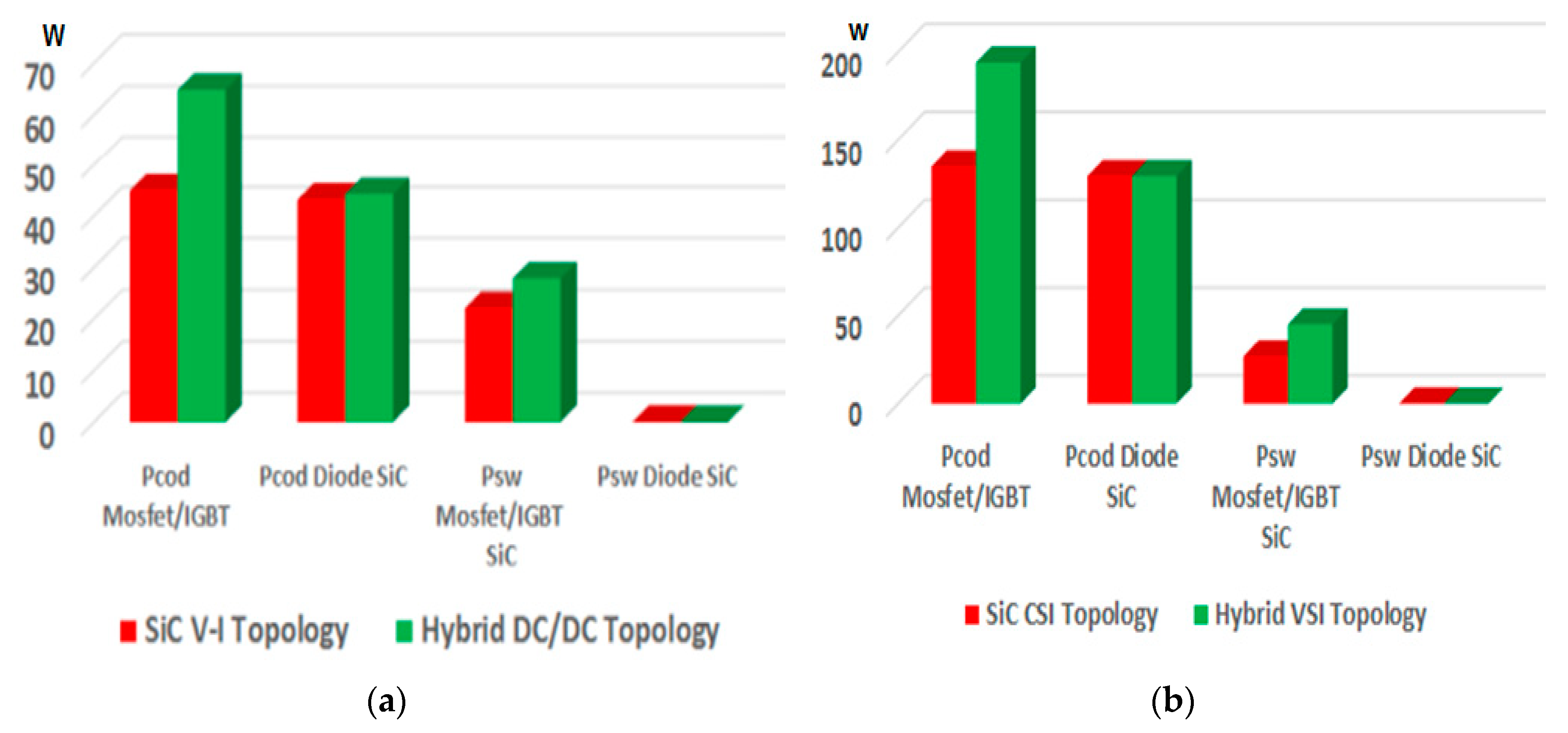
Figure 26.
Results in VSI topology. (a) Current of output in VSI topology. (b) THD spectrum result for 6.76%.
Figure 26.
Results in VSI topology. (a) Current of output in VSI topology. (b) THD spectrum result for 6.76%.

Table 1.
Parameters of simulations of the PI control.
| Parameter | Values |
|---|---|
| Kp | 4.75769580834167 |
| Ki | 460.186624758197 |
| Rise time | 0.00488 s |
| Settling time | 0.00838 s |
| Overshoot | 0.0198% |
| Peak | 1 |
| Phase margin | 889 deg @ 439 rad/s |
Table 2.
Parameters of simulations.
| Parameter | Values |
|---|---|
| Vdc | 100 V |
| Current | 10 A |
| Inductor L1 | 10 mH |
| Frequency Fs | 35 kHz |
| Capacitor C1, C2, C3 | 1 5 μF |
| Index of Modulation m | 0.8 |
| L Load | 1.5 mH |
| R Load | 1.3 Ω |
Table 3.
THD result with angle-shift and sequence.
| Angle of Shift | Values of THD | Sequence ON OFF |
|---|---|---|
| 0° | 2.10% | C*CC*CC|C*CC*CC |
| 30° | 2.22% | CC*CC*C|CC*CC*C |
| 60° | 2.39% | *CC*C*C|*CC*C*C |
| 90° | 1.98% | C*CC*CC|C*CC*CC |
| 120° | 2.25% | *CC*CC*|*CC*CC* |
| 150° | 2.13% | C*CCC*C|C*CCC*C |
| 180° | 2.15% | CC*C*CC|CC*C*CC |
Table 4.
Result of THD with an angle shift.
| Shift-Angle | Values of THD |
|---|---|
| 0° | 2.29% |
| 90° | 2.74% |
| 120° | 2.45% |
Table 5.
Parameters of simulations.
| Parameter | Mosfet SiC | Parameter | Diode SiC |
|---|---|---|---|
| Model | SCT2450KE | Model | C3D10065I |
| Voltage DS | 1200 V | VRRM (V) | 650 V |
| Current | 10 A | QC (nC) | 110 nC |
| Rds | 450 mΩ | IF (A) | 10 A |
| Power Dissipation | 85 W | ||
| Operating Junction | 175 °C |
Table 6.
Inductor core losses.
| Parameter | Value |
|---|---|
| Hysteresis losses | 0.0517 W/cm3 |
| Eddy current losses | 0.2738 W/cm3 |
| Copper losses | 29.93 W/cm3 |
| Total of losses in the inductor | 30.255 W/cm3 |
Table 7.
Parameters of simulations.
| System | Efficiency at 0° | Efficiency at 90° | Power Out |
|---|---|---|---|
| V-I | 88.25% | 90.1% | 1 kW |
| CSI | 93.8% | 94.22% | 1.5 kW |
| Motor | 91.2% | 91.38% | 1.5 kW |
| Average | 91.08% | 92% | 1.5 kW |
Table 8.
Parameters of simulations.
| Parameter | Mosfet SiC | Parameter | Diode SiC |
|---|---|---|---|
| Model | HGTG30N60BD3 | Model | C3D10065I |
| Voltage CE | 600 V | VRRM (V) | 650 V |
| Current | 15 A | QC (nC) | 110 nC |
| Power Dissipation | 208 W | IF (A) | 10 A |
| Operating Junction | 150 °C |
Table 9.
Power losses between SiC topology and Hybrid Topology.
| Parameter | All-SiC Topology V-I–CSI | Hybrid Topology DC/DC–VSI | ||
|---|---|---|---|---|
| Pconduction Mosfet SiC/IGBTs | 44.98 W | 134.94 W | 64.9 W | 194.24 W |
| Pconduction diodes | 43.16 W | 129.48 W | 44.57 W | 129.42 W |
| Pswitching SiC/IGBTs | 22.87 W | 26.88 W | 27.88 W | 45.08 W |
| Pswitching diodes | 0.0296 W | 0.178 W | 0.0006 W | 0.036 W |
| Total | 402.51 W | 506.29 W | ||
© 2018 by the authors. Licensee MDPI, Basel, Switzerland. This article is an open access article distributed under the terms and conditions of the Creative Commons Attribution (CC BY) license (http://creativecommons.org/licenses/by/4.0/).
Share and Cite
MDPI and ACS Style
Fernández, E.; Paredes, A.; Sala, V.; Romeral, L. A Simple Method for Reducing THD and Improving the Efficiency in CSI Topology Based on SiC Power Devices. Energies 2018, 11, 2798. https://doi.org/10.3390/en11102798
AMA Style
Fernández E, Paredes A, Sala V, Romeral L. A Simple Method for Reducing THD and Improving the Efficiency in CSI Topology Based on SiC Power Devices. Energies. 2018; 11(10):2798. https://doi.org/10.3390/en11102798
Chicago/Turabian StyleFernández, Efrén, Alejandro Paredes, Vicent Sala, and Luis Romeral. 2018. "A Simple Method for Reducing THD and Improving the Efficiency in CSI Topology Based on SiC Power Devices" Energies 11, no. 10: 2798. https://doi.org/10.3390/en11102798
Note that from the first issue of 2016, this journal uses article numbers instead of page numbers. See further details here.