Review

A Comprehensive Review of One-Dimensional Metal-Oxide Nanostructure Photodetectors

1
World Premier International Center for Materials Nanoarchitectonics (MANA), National Institute for Materials Science (NIMS), Namiki 1-1, Tsukuba, Ibaraki 305-0044, Japan
2
Sensor Materials Center, National Institute for Materials Science (NIMS), Namiki 1-1, Tsukuba, Ibaraki 305-0044, Japan
*
Authors to whom correspondence should be addressed.
#
These authors contributed equally to this work.
Sensors 2009, 9(8), 6504-6529; https://doi.org/10.3390/s90806504
Submission received: 14 July 2009 / Revised: 5 August 2009 / Accepted: 19 August 2009 / Published: 20 August 2009
(This article belongs to the Special Issue Metal-Oxide Based Nanosensors)

Abstract

:
One-dimensional (1D) metal-oxide nanostructures are ideal systems for exploring a large number of novel phenomena at the nanoscale and investigating size and dimensionality dependence of nanostructure properties for potential applications. The construction and integration of photodetectors or optical switches based on such nanostructures with tailored geometries have rapidly advanced in recent years. Active 1D nanostructure photodetector elements can be configured either as resistors whose conductions are altered by a charge-transfer process or as field-effect transistors (FET) whose properties can be controlled by applying appropriate potentials onto the gates. Functionalizing the structure surfaces offers another avenue for expanding the sensor capabilities. This article provides a comprehensive review on the state-of-the-art research activities in the photodetector field. It mainly focuses on the metal oxide 1D nanostructures such as ZnO, SnO2, Cu2O, Ga2O3, Fe2O3, In2O3, CdO, CeO2, and their photoresponses. The review begins with a survey of quasi 1D metal-oxide semiconductor nanostructures and the photodetector principle, then shows the recent progresses on several kinds of important metal-oxide nanostructures and their photoresponses and briefly presents some additional prospective metal-oxide 1D nanomaterials. Finally, the review is concluded with some perspectives and outlook on the future developments in this area.

1. Introduction

One-dimensional (1D) nanomaterials have stimulated great interest due to their importance in basic scientific research and potential technological applications [13]. It is generally accepted that 1D nanostructures are ideal systems for exploring a large number of novel phenomena at the nanoscale and investigating the size and dimensionality dependence of structure properties for potential applications [4]. 1D nanomaterials are also expected to play an important role as both interconnects and functional units in fabricating electronic, optoelectronic, electrochemical, and electromechanical devices with nanoscale dimensions [5]. Among the inorganic semiconductor nanomaterials, 1D metal oxide nanostructures are the focus of current research efforts in nanotechnology since they are the most common minerals on the Earth due to their special shapes, compositions, and chemical, and physical properties. They have now been widely used in many areas, such as transparent electronics, piezoelectric transducers, ceramics, catalysis, sensors, electro-optical and electro-chromic devices [68]. Doubtlessly, a thorough understanding of the fundamental properties of a 1D metal oxide system is prerequisite in research and development towards practical applications.
Table 1 shows the fundamental physical properties of some important metal-oxide semiconductors, including zinc oxide (ZnO), tin dioxide (SnO2), copper oxide (Cu2O), Gallium oxide (β-Ga2O3), Hematite (α-Fe2O3), Indium oxide (In2O3), Cadmium oxide (CdO) and Ceria (CeO2).
Among all nanoscale devices, the photodetectors are critical for applications as binary switches in imaging techniques and light-wave communications, as well as in future memory storage and optoelectronic circuits [10,11]. With large surface-to-volume ratios and Debye length comparable to their small size, these 1D nanostructures have already displayed superior sensitivity to light in experimental devices. Until now, various 1D metal-oxide nanostructures have been used for the fabrication of photodetectors, and the related mechanism has been investigated over the years. This mechanism is outlined below, using ZnO nanowire (NW) as a model system. Essentially, all experiments carried out to date on metal-oxide nanostructures indicated that the role of oxygen vacancies is predominant for the electronic properties, similar to the bulk systems [8].
As discussed by Yang et al, Wang et al and other groups [9,1214], in the dark, the oxygen molecules absorb on the ZnO NW surface and capture the free electrons present in a n-type oxide semiconductor [ O 2   ( g ) + e O 2   ( ad )], and a low-conductivity depletion layer is formed near the surface (Figure 1b), that results in the reduction of the channel conduction. When the ZnO NW is illuminated by a UV-light whose photon energy is above the energy gap (Eg) of the ZnO, then the electron-hole pairs are photogenerated [e + h+], and the holes migrate to the surface along the potential slope produced by band bending and discharge the negatively charged absorbed oxygen ions through surface electron-hole recombination [ h + + O 2   ( ad ) O 2   ( g )]. Consequently, oxygen is photodesorbed from the surface. The unpaired electrons are either collected at the anode or recombine with holes generated when oxygen molecules are reabsorbed and ionized at the surface. The hole-trapping mechanism through oxygen desorption in ZnO NWs augments the high density of trap states (usually found in NWs) due to the dangling bonds at the surface, and thus greatly increases the NW photoconductivity [9]. With respect to a traditional film photodetector, 1D metal-oxide nanostructures have several advantages. namely a large surface-to-volume ratio with the carrier and photon confinement in two dimensions, superior stability owing to high crystallinity, possible surface functionalization with target-specific receptor species, and field-effect transistor configurations that allow the use of gate potentials controlling the sensitivity and selectivity [15].
This article provides a comprehensive review of the state-of-the-art research activities that focus on several kinds of important metal-oxide nanostructures such as ZnO, SnO2, Ga2O3, Cu2O, Fe2O3, In2O3, CdO, CeO2, and their corresponding photodetector applications, and briefly discusses some other metal-oxide semiconductors. In the end, we conclude this review with some perspectives/outlook and future research directions in this field.

2. Different Photodetector Materials—Metal Oxides

In this section, we highlight recent progresses with respect to several kinds of metal-oxide nanostructures, including ZnO, SnO2, Ga2O3, Fe2O3, In2O3, CdO, Cu2O and CeO2, and their photoresponses.

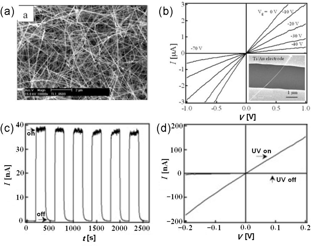
2.1. ZnO-Based Photodetectors

ZnO is one of the most prominent semiconductors in the metal-oxide family. It has a wide-band-gap of 3.37 eV and a large exciton binding energy of 60 meV. This ensures efficient excitonic ultraviolet (UV) emission at room temperature. Besides, the non-central symmetry of ZnO in wurtzite structure, combined with its large electromechanical coupling, results in strong piezoelectric and pyroelectrical properties and implies a consequent usage in actuators, piezoelectric sensors and nanogenerators. ZnO is also bio-safe, biocompatible, and can be directly used for biomedical applications without coatings [4]. As for 1D ZnO nanostructures, they play the key roles in developing nanoscience and nanotechnology, as illustrated by many articles published. It is fair to state that ZnO 1D nanostructures are probably the most important Metal-Oxide-Semiconductor 1D nanostructures in nowadays research. Growing interests in the synthesis of ZnO nanostructures are stimulated due to promising applications in nanoscale technologies and devices. ZnO diverse and versatile morphologies are probably wider than any other materials known to date [16,17].
In this section, we will first give two examples related to “Nanowire Ultraviolet Photodetectors and Optical Switches”, and “Photoswitches and Memories Assembled by Electrospinning Aluminum-Doped Zinc Oxide Single Nanowires”, and then report the systematic investigations on photodetector applications based on ZnO nanostructures. In 2002, Yang and coworkers first found that the conductance of ZnO NW had been extremely sensitive to ultraviolet light exposure [12]. The light-induced conductivity enabled them to reversibly switch the NWs between OFF and ON states. In a typical experiment, four-terminal measurements on an individual ZnO structure indicated that they were almost insulating in the dark with a resistivity of ∼3.5 MΩ cm−1. When the NWs were exposed to 365 nm UV-light, their resistivity was remarkably reduced by 4–6 orders of magnitude, as shown in Figure 2a. Furthermore, the NW photodetector exhibited strong power dependence (Figure 2b) and excellent wavelength selectivity (Figure 2c) [12].
Yang et al. further evaluated the NW potential in optoelectronic switches, with the insulating state as “OFF” state in the dark, and the conductance state as “ON” when exposed to UV light. Figure 2d plots the photoresponse of a ZnO NW as a function of time while the UV-light was switched on and off. It is evident that this NW could be reversibly and rapidly switched between the low- and high-conductivity states. The rise and decay times of the fastest NW switches were below the apparatus detection limit, which was roughly 1 s [5,12].
After that, several researchers have dedicated themselves to improving the response of a ZnO 1D nanostructure photodetector, and obtained a series of remarkable achievements. He and coauthors utilized focused-ion-beam (FIB) technique to deposit Pt metal on ZnO NWs and transmission-line-method (TLM) measurements to effectively reduce the contact resistance which was as low as 1.1 × 10⁵ Ωcm2, and thus achieved ZnO NW-based UV photodetectors with a photoconductive gain as high as 108 (the photoconductive gain is one of the most important physical parameters which determines the photocarrier collection efficiency) [13].
Prades and coauthors presented a set of criteria to optimize a ZnO NW photodetector. They enhanced its response through different fabrication strategies, such as diminishing the distance between the electrical contacts, increasing the width of the photoactive area, or improving the electrical mobility of the nanomaterials [18]. Very recently, Kim and coauthors demonstrated that drain-source (Vds) and gate-source voltages (Vgs) of a ZnO NW FET could be optimized to increase UV photodetection sensitivity. They found that the detector was the most sensitive when it was operated with the highest on/off current ratio and at the “bottom” of the sub-threshold swing region. Their photodetector showed maximum photo- to dark- current ratio of ∼106 upon UV illumination near Vgs = −1 V and Vds = 1 V. These results could be applied to improve sensitivity of other kinds of FET-based photodetectors whose sensing mechanism is based on the change of carrier concentration [19].
Recently, several doped 1D ZnO nanostructures have been synthesized and investigated for enhancing and controlling ZnO nanostructures’ mechanical, electrical and optical performances. Pan et al. reported on a photoconductor device that was sensitive to illumination with below-gap light by electrospinning a single Al doped-ZnO (AZO) nanowire. By using a “Cu bridge” as the cathode (Figure 3a), the electrospun nanowires could be uniaxially aligned over long length scales during the e-spinning process. The nanowires were then directly transferred to a SiO2/Si substrate, and calcined at 550 °C for 3 h to obtain well-aligned polycrystalline AZO nanowires. A typical I-V curve for a single AZO nanowire with different Al concentrations is shown in Figure 3b. Compared with the pure ZnO nanowires with a conductivity of 2.55×10⁻⁵ S/cm, the Al-doped ZnO nanowires show a steep increase up to 9.73 × 10⁻³ S/cm (Al = 5%), indicating a great enhancement in conductivity. Alumina acts as a cationic dopant in the ZnO lattice, that is, the trivalent Al3+ ion occupies the divalent Zn2+ site ( Al Zn ) allowing electrons to move to the conduction band easily.
Figure 3c shows the I–V curves measured in dark and under illumination for comparison. As the device was illuminated by a white-light source with ∼400–800 nm, the conductance of an individual AZO (Al ∼1.0 at %) nanowire increased significantly from 3.36 × 10⁻⁴ S/cm to 6.67 × 10⁻³ S/cm, which is about 20 times of that measured in darkness. The authors suggest that the notable photoresponse of the AZO nanowires may be attributed to photo-excitation of electrons from the defect levels introduced by Al doping. As light with energy below the bandgap is introduced, the electrons captured at the detect states, such as Al Zn , V Zn , as well as an impurity band of ca. 80 meV binding energy below the effective band edge of ZnO, are photo-excited to the conduction band, as illustrated in Figure 3d.
The increase in carrier density thus greatly enhances the conductivity of the AZO nanowire. In contrast, an extremely weak photoresponse of undoped ZnO nanowires was observed, with only a small current rise of about 6.4% [20]. Very recently, Xie et al. have found a negative photoconductivity of Co-doped ZnO nanobelts. The decrease of photoconductivity from 1.3 to 0.25 μA in ambient air or water vapor atmosphere is observed when the Co-doped ZnO nanobelts are irradiated with 630 nm light. The authors think that this kind of negative photoconductivity is attributed to the photodesorption of water molecules from nanobelts’ surface [28]. Meanwhile, Kouklin et al. reported the fabrication of Cu-doped ZnO nanowires for efficient and multispectral photodetection applications. The use of Cu is shown to dramatically enhance the photosensitivity levels of the nanowires to both UV and visible light as a result of avalanche photomultiplication [38].
It should be stated that within last few years, tremendous progress has already been made in photodetector applications of ZnO 1D nanostructures. For instance, we realized that there have been more than 50 research papers published solely related to ZnO 1D nanostructure photodetector characteristics. Here, we tabulate the representative results on photodetector properties of ZnO nanostructures reported so far, along with a brief description of the corresponding device continuations, detection wavelength, and photodetector performance (Table 2).

2.2. SnO2-Based Photodetectors

SnO2, as another important n-type metal-oxide semiconductor, is particularly interesting and has many important applications. Its large bandgap (Eg = 3.6 eV at 300 K) makes it ideally working as a transparent conducting electrode for organic light emitting diodes and solar cells [46,47]. In addition, SnO2 films and nanostructures have extensively been studied and used as chemical sensors for environmental and industrial applications.
Zhou et al. reported the preparation of SnO2 NWs using a laser-ablation technique. The NW diameters can be precisely controlled by using mono-dispersed gold clusters as the catalyst. Most of the NWs have diameters around 20 nm and lengths of the order of 10 μm, as illustrated in Figure 4a. Field-effect transistors were made based on these SnO2 NWs, and n-type transistor characteristics were recorded with threshold voltages of 50 V and on/off ratios of 103 at room temperature. The authors also investigated the photoresponse properties of a SnO2 NW transistor. As shown in Figure 4c, the current increased dramatically and stabilized a high-conductivity “on” state (∼760 nS) upon UV exposure; whereas it decreased quickly and ended up at a low-conductivity “off” state (∼0.66 nS) after the UV light was blocked, leading to an on/off ratio as high as 103. The response time of this device was less than 0.1 s [46]. To date, there have been only a few reports that deal with photodetector properties of 1D SnO2 nanostructures, as shown in Table 3.

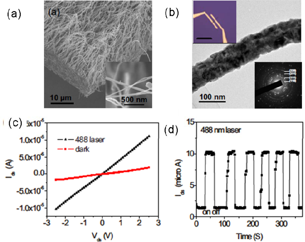
2.3. Cu2O-based photodetectors

Copper oxide (Cu2O) is one of the first known p-type direct band gap semiconductors. It has the advantages of nontoxicity, low cost, availability, high absorption coefficients at 2.17 eV, and energy conversion efficiencies [49]. Its outstanding excitonic properties including a large exciton binding energy (∼150 meV) have been the target of the most of research efforts during the past decades. Due to their unique physical and chemical properties, Cu2O materials have found prominent applications in field-effect transistors, photovoltaic devices, sensors, and photo-electrodes in high-efficiency photo-electrochemical cells [48,50].
Yu et al. reported that Cu2O NWs could be conveniently synthesized by reduction of CuO NWs in hydrogen gas. The SEM image shows that the prepared aligned Cu2O NWs on the substrate are ∼20–30 μm in length and ∼50–100 nm in diameter. A typical TEM image of the Cu2O NWs is shown in Figure 5b. A selected area diffraction pattern of the NW reveals that it is polycrystalline. Figure 5c shows I–V characteristics of the Cu2O NW, measured in dark room and under blue light (488 nm) laser illumination. As known, photogenerated carriers could significantly increase the conductivity when semiconductor materials are illuminated by high energy photons. Meanwhile, the large surface to volume ratio of semiconductor NWs is able to further enhance the sensitivity of the NW device to light and even possibly lead to the realization of single photoconductivity. Thus the conductance of NW increased from 0.7 to 4.3 μS under the illumination. Time-resolved measurements of the photoresponse to a 488 nm light were conducted and the results are shown in Figure 5d. The “on” current and “off” current for each of six cycles remains the same within the noise envelope, indicating the reversibility and stability of the Cu2O NWs optical switches. The photoconductivity response time is less than three seconds. These results show that the Cu2O NW devices have a fast photoresponse to blue illumination in air and at room temperature [48].

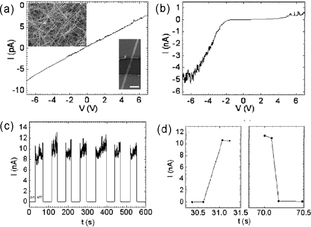
2.4. Ga2O3-based photodetectors’

Monoclinic gallium oxide (β-Ga2O3) is a promising oxide semiconductor with a wide direct hand gap of 4.9 eV [52,53]. It is chemically and thermally stable and has been widely used as an insulating oxide layer in gallium-based electrical devices. β-Ga2O3 is an n-type semiconductor at elevated temperatures and its semiconductivity is governed by an oxygen deficiency of the crystal lattice [54]. With its surprising bulk properties, such as conduction and luminescence, this material can be applied for high temperature gas sensing, solar cells, flat-panel displays and optical limiters for ultraviolet irradiation [55].
Recently, an individual β-Ga2O3 NW as a solar-blind photodetector was investigated by Wang and coworkers. The SEM image depicts the general morphology of β-Ga2O3 NWs. They have diameters of several tens of nanometers and length of a few tens of micrometers. I–V curves of the photodetector device without and under 254 nm light illumination are shown in Figures 6a and 6b. As the device is exposed to illumination by an ultraviolet lamp, its conductance greatly increases. Due to the poor ohmic contacts between the electrodes and the NWs, the I–V curve of the device under illumination is asymmetric and nonlinear. Figure 6d shows the real-time response of the detectors to 254 nm light by ON/OFF switching at a bias of −8 V. It can be seen that the dark current is of the order of pA. Upon illumination, the current rapidly increases to several nA, but the current fluctuations are a little larger (maybe due to the surface species absorption/desorption or appearance of defects). As the light is off, the current suddenly decreases to its original value. The detectors operated with an upper limit of the response time of 0.22 s, an upper limit of the recovery time of 0.09 s, and a sensitivity of ∼1000. These results demonstrate that β-Ga2O3 NWs are promising materials for realizing solar-blind photodetectors [51].

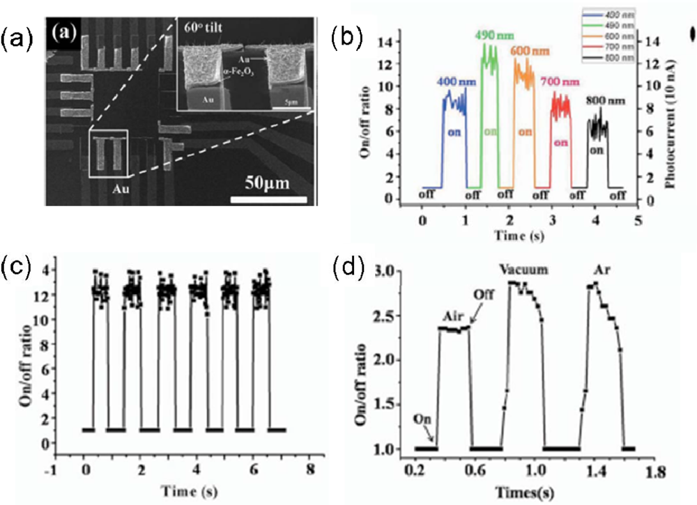
2.5. Fe2O3-based photodetectors

Hematite (α-Fe2O3) is a stable n-type semiconductor with unique magnetic properties and thermal stability. Due to its narrow band gap of 2.1 eV, α-Fe2O3 NWs were applied in water splitting and solar cells [56].
Li et al. for the first time reported a visible light photodetector made of an individual α-Fe2O3 NW. The authors introduced a simple thermal oxidation process to form an individual α-Fe2O3 nanobridge (NB) photodetector with a diameter of 8 nm between the electrodes on a Si3N4/Si substrate. From the SEM (Figure 7a) and TEM images, it is understood that the NWs had been grown laterally from one side of the Fe film to another, which acted as a NB to connect the two patterns. The diameter and the length of an individual NB were ∼8 nm and ∼240 nm, respectively. HRTEM and SAED results demonstrated that the NWs are crystallized in a rhombohedral structure with the growth direction along the [110]. The photocurrent properties of an individual α-Fe2O3 NB device were then investigated in detail. The photocurrent can be enhanced by illumination at 400–800 nm (visible light). The maximum photocurrent was ∼123 nA at ∼490 nm. As shown in Figure 7b, the on/off ratios were ∼12 for 490 nm and 11 for 600 nm, and the response time for the visible light was less than 20 ms. The gain of the α-Fe2O3 NB device was calculated to be 2.9 × 10⁷. The authors also investigated the response of the on/off ratio with or without illumination in air, Ar or vacuum. The measured photocurrents and response time were both increased in oxygen-free environment (under vacuum or Ar) as shown in Figure 7d [56].

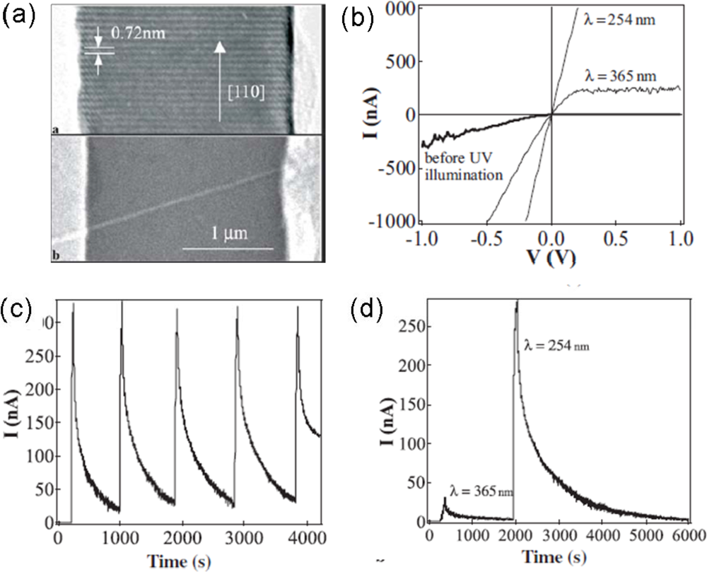
2.6. In2O3-Based Photodetector

In2O3 is a wide-bandgap transparent semiconductor (with a direct bandgap of ∼3.6 eV and an indirect bandgap of ∼2.5 eV). In its bulk form, the material has been widely used in solar cells and organic light-emitting diodes. More importantly, In2O3 films have been demonstrated to work as ultra-sensitive toxic-gas detectors with detection levels down to 5 ppm for NO2, due to the surface interaction and electron transfer between NO2 molecules and In2O3 surface. 1D In2O3 nanostructures are expected to offer enhanced sensitivity and an improved response time due to the increased surface-to-volume ratios. Zhou’s group has conducted an excellent work on the fabrication, electronic transport and ultraviolet photodetection properties of In2O3 NWs [5759]. The In2O3 NWs were synthesized using a laser ablation technique via the vapor-liquid-solid mechanism. The SEM and TEM results show that these NWs have well-controlled diameters of 10 nm and lengths exceeding 3 μm. The HRTEM image demonstrates that the NWs have single-crystalline structures grown along the [100] direction. Devices based on individual In2O3 NW display a substantial increase in conductance (of up to four orders of magnitude) upon exposure to UV light, as shown in Figure 8b. Figure 8d presents the time response of the device after its exposure to the 365 nm and 254 nm lights sequentially. UV light with a wavelength of 365 nm brought a current to ∼33 nA. Significantly stronger conduction (290 nA) was observed upon exposure to a 254 nm UV light. The differences in conductions are attributed to different excited models. The photo energy of 254 nm (4.9 eV) light is larger than the In2O3 direct bandgap (3.6 eV). This sufficiently excites electrons directly from the valence band to the conduction band. In contrast, the photo energy for a 365 nm light is smaller than that of In2O3 NWs but larger than the indirect energy gap of 2.5 eV. This results in the indirect transitions. Furthermore, the authors have also demonstrated that the UV light can be used as a “gas cleaner” for In2O3 NW chemical sensors, leading to a recovery time as short as 80 s [57]. However, as a photodetector, the dark decay time of this In2O3 device operated at 254 nm is a little longer.

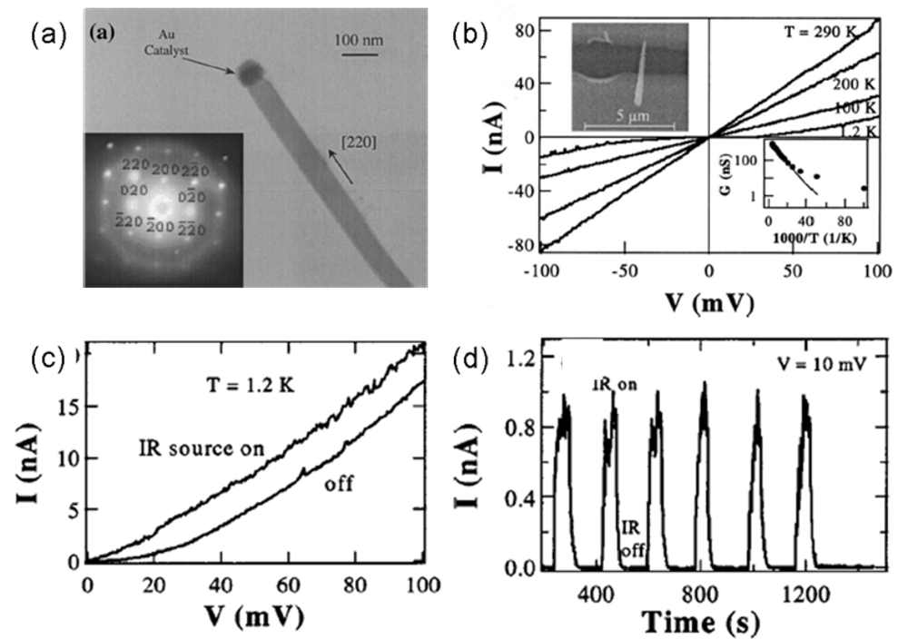
2.7. CdO-Based Photodetectors

Among conductive oxide (TCO) materials CdO shows a high promise. It exhibits a wide direct band gap of 2.27 eV and a narrow indirect band gap of 0.55 eV. Several techniques have been used to grow 1D CdO nanostructures, such as nanowires, nanobelts, and nanoneedles. Figure 9a shows a TEM image of a single CdO nanoneedle grown by VLS mechanism under a chemical vapor deposition process. The SAED pattern demonstrates that the CdO nanoneedles are single crystals with a cubic crystal structure grown along the [220] direction. The electrical transport and photoresponse properties were studied by fabricating electrodes onto individual nanoneedles, as illustrated in Figure 9b. Electrical properties were measured at different temperatures, revealing that the transport is dominated by thermal excitation. These CdO nanoneedle devices can absorb IR light via the indirect band gap mechanism rather than under the direct band gap process. The IR detection on/off ratio is ∼8.6 at 1.2 K and the relaxation time constant is estimated to be 8.6 s [60]. The experiments on IR detectors were carried out at 1.2 K to minimize the thermal excitation. These results indicate that these IR detectors may only work at low temperatures, not at room temperature, which will restrict its practical application.

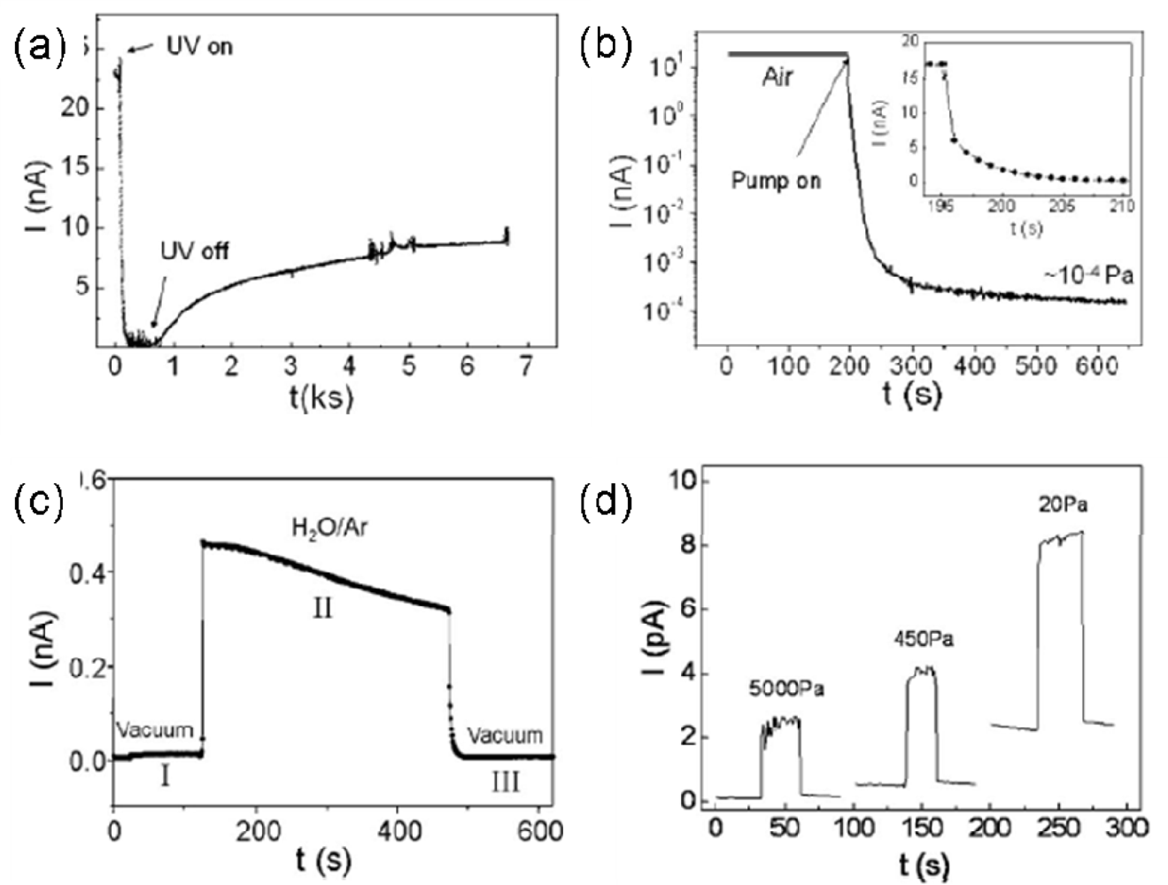
2.8. CeO2-Based Photodetectors

As a well-known functional rare earth material, CeO2 has widely been applied in many fields such as catalysts, gas sensors and optics due to its unique properties. It has strong absorption in the UV region and is used as a UV blocking and shielding material [62]. Wang et al. reported the fabrication of CeO2 NWs via a wet chemical route. These NWs, with diameters of 20–40 nm and lengths of several micrometers, were dispersed on interdigital electrodes. As shown in Figure 10a, the dark current is ∼22.8 nA in air; in contrast, upon exposure to UV illumination, the current decreases rapidly to 10 nA and then gradually decreases to 0.25 nA in 300 s, which is different from the traditional photodetectors. The authors also investigated the photoresponse behavior of the device in vacuum, H2O/Ar mixed gas and different dry O2 pressure conditions, as depicted in Figures 10c and 10d. As the pressure decreases (air to vacuum), the current decreases by nearly five orders of magnitude, from 17.1 to 1.6 × 10⁻⁴ nA. When H2O/Ar mixed gas and O2 are introduced into the chamber, the photocurrent increases rapidly. The authors suggested that this anomalous behavior, i.e., negative CeO2 NWs photoconductivity in air, was due to UV-induced desorption of H2O from the nanowire’s surface [61]. In regard of the photodetector application, the on-off ratio of the CeO2 device is a little lower and the response time is a little longer.

2.9. Ternary Oxide-Based Photodetectors

2.9.1. ZnSnO3-based photodetectors

Yue et al. reported the photoconducting properties of individual ZnSnO3 NWs by performing transport measurements under UV and green laser illumination on/off circles [63]. For their experiments, the ZnSnO3 NWs were synthesized by thermal evaporation of ZnO, SnO and graphite mixed powders. Such NWs possessed core-shell structures. Upon exposure to UV illumination, the current of an individual ZnSnO3 NW increases by about three orders of magnitude, from 0.3 nA to 162 nA within 20 s. And the current increases to 6.6 nA in 20 s under green laser illumination. Such behavior was ascribed to a fact that the illuminations adjusted the grain boundary barrier (that between the core and the shell) [63].

2.9.2. ZnGa2O4-based photodetectors

Zinc gallate (ZnGa2O4), with a band gap of 4.4–4.7 eV, is potentially of great technological interest for the development of luminescence, vacuum electronics and multicolor emitting phosphors. The material has received a significant attention [64]. Feng et al. fabricated ZnGa2O4 NWs via a low-pressure chemical vapor deposition method using Ga metal and ZnO nanopowders as the sources and investigated the electrical transport. The NWs have diameters of several tens of nanometers and lengths of a few tens of micrometers. It was found that the current across individual NW was several pA at a bias of 30 V, and the current was sensitive to oxygen and temperature. These behaviors were still maintained as the ZnGa2O4 NWs were exposed to below-band-gap irradiation. In contrast, upon exposure to a 254 nm UV light, the current drastically increased. With decreasing oxygen pressure or increasing temperature, the photocurrent also increased. The authors demonstrated that the surface-related processed (especially oxygen chemisorptions) had significant effects on the nanostructure photoelectronic properties [64].

2.9.3 RuO2/TiO2 core/shell nanowire-based photodetectors

Chou et al. reported the fabrication of RuO2/TiO2 core/shell NWs by reactive sputtering, and investigated photoconductive properties [65]. These core-shell NWs had a square-like cross section and lengths of several micrometers. Upon exposure to a 256 nm UV light, the current of the RuO2/TiO2 core/shell structure rapidly increased, from 18.5 μA to 19.4 μA within 88 s, and then slowly increased to become saturated at 20 μA within 219 s during the first illumination. After the UV light was turned off, the current decreased from 20 μA to 19.4 μA within 52 s and then slowly recovered to the original value (under 385 nm illumination). The authors noted that the current decay rate was faster than the current increment rate. This was explained by a fact that water and oxygen molecules fast adsorbed on the surface via physiabsorption and chemiabsorption because of the large surface-to-volume ratio. The process resulted in a drastic drop in conductance as the UV light was turned off [65].

3. Conclusions and Outlook

In summary, this article provides a comprehensive review on recent advances in some important 1D metal-oxide nanostructures and their photodetector properties. Tables 2 and 3 are the up-to-date summaries of most important reports on photodetectors made of several metal-oxide nanostructures. Needless to say, due to the tremendous research efforts and the space limitations, this article is unable to cover all the exciting works reported in this field.
It is noted that photoconductors based on 1D metal-oxide nanostructures have acquired fascinating achievements just in the last 10 years. However, the ways towards their practical applications are still endless and tortuous. This should inspire more research efforts to address the challenges that remain, as noted below:
  • Nanomaterial fabrication: As known, the material is the milestone of a device. The growth kinetics and thermodynamics involved in the synthesis of metal-oxide nanostructures are extremely complex, and presume different mechanisms under different growth conditions. Although comprehensive efforts have been made towards the synthesis of high-quality metal-oxide nanostructures, significant challenges still exist in their syntheses that include, but not limited to, reliable control of diameter, length, orientation, density, crystallization and hierarchical assembly.
  • Device fabrication: In the conventional “pick and place” method, 1D nanostructures fabricated by vapor synthesis process are first collected from substrates on which they were initially grown and then, dispersed randomly on an insulating substrate after being diluted in a solution. Sophisticated techniques such as photolithography, electron beam lithography or focused ion beam are required to make metallic contacts to the nanostructures. Out of question, this process is complicated, time-consuming and uneconomic, thus hampering the development of practical routes [21]. It still remains a grand challenge to construct a device via a simple and effective method. Furthermore, since the performance of devices critically depends on the quality of the Ohmic contacts between a nanostructure and the electrodes, the construction of reliable and stable contacts is an urgent task that deserves particular attention.
  • Sensitivity, selectivity and stability (3S): Next generation photodetectors will require significant improvements in sensitivity, selectivity and stability (3S) in order to meet the future demands in variety of fields. Though some research groups have successfully detected light using 1D metal oxide nanostructures, the selectivity and stability are still quite low.
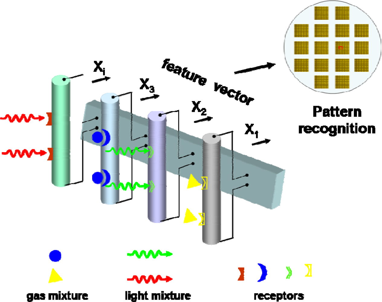
  • Multi-functional detectors: The evolution of photodetectors goes in parallel with the development of microelectronics in which the architecture of photodetector elements is influenced by design trends in planar electronics. One of the major goals is to design nanodetectors that could be easily integrated into modern electronic fabrication technologies [8]. A possible avenue to differentiate the 1D nanostructure response maybe surface coating with chemical selective membrane, surface medication by specific functional groups, or combing multi-light and/or multi-gas sensing modules coupled with signal processing functions, acting as an “electronic nose” to differentiate in a more complex environment (Figure 11).
There is still plenty of room for the development of 1D metal-oxide nanostructures and their photodetector applications. We believe that future work in this direction should continue to focus on generating metal oxide nanostructures in a more controlled, predictable, reliable and simple way, and enhancing their photoconductor properties up to the level desirable in real industrial applications. The hopes are high that significant practical photodetector devices will soon arise due to the integration of 1D metal oxide nanostructures into conventional microelectronics.

Acknowledgments

This work was supported by the Japan Society for Promotion of Science (JSPS) in the form of a fellowship tenable at the National Institute for Materials Science (NIMS), Tsukuba, Japan (T. Y. Zhai). This work was also in part supported by the World Premier International Center for Materials Nanoarchitectonics (MANA) of the National Institute for Materials Science (NIMS), MEXT, Japan. The authors are indebted to Profs. D. Wang, P.D. Yang, C.W. Zhou, T. Yu, Y. Y. Li, T.H. Wang, A. Kolmakov, and M. Moskovits for their cooperation, kind help and offering some useful materials for the preparation of this review.

References and Notes

  1. Yang, P.D.; Yan, H.Q.; Mao, S.; Russo, R.; Johnson, J.; Saykally, R.; Morris, N.; Pham, J.; He, R.; Choi, H.J. Controlled growth of ZnO nanowires and their optical properties. Adv. Mater 2002, 12, 323–331. [Google Scholar]
  2. Zhai, T.Y.; Zhong, H.Z.; Gu, Z.J.; Peng, A.D.; Fu, H.B.; Ma, Y.; Li, Y.F.; Yao, J.N. Manipulation of the morphology of ZnSe sub-micro structures using CdSe nanocrystals as the seeds. J. Phys. Chem. C 2007, 111, 2980–2986. [Google Scholar]
  3. Lieber, C.M.; Wang, Z.L. Functional nanowires. MRS Bull 2007, 32, 99–104. [Google Scholar]
  4. Fang, X.S.; Bando, Y.; Gautam, U.K.; Ye, C.H.; Golberg, D. Inorganic semiconductor nanostructures and their field-emission applications. J. Mater. Chem 2008, 18, 509–522. [Google Scholar]
  5. Xia, Y.N.; Yang, P.D.; Sun, Y.G.; Wu, Y.Y.; Mayers, B.; Gates, B.; Yin, Y.D.; Kim, F.; Yan, H.Q. One-dimensional nanostructures: synthesis, characterization and applications. Adv. Mater 2003, 15, 353–389. [Google Scholar]
  6. Shen, G.Z.; Chen, P.C.; Ryu, K.; Zhou, C.W. Devices and chemical sensing applications of metal oxide nanowires. J. Mater. Chem 2009, 19, 828–839. [Google Scholar]
  7. Lu, J.G.; Chang, P.C.; Fan, Z.Y. Quai-one-dimensional metal oxide materials-synthesis, properties and applications. Mater. Sci. Eng. R 2006, 52, 49–91. [Google Scholar]
  8. Kolmakov, A.; Moskovits, M. Chemical sensing and catalysis by one-dimensional metal-oxide nanostructures. Annu. Rev. Mater. Res 2004, 34, 151–180. [Google Scholar]
  9. Soci, C.; Zhang, A.; Xiang, B.; Dayeh, S.A.; Aplin, D.P.R.; Park, J.; Bao, X.Y.; Lo, Y.H.; Wang, D. ZnO nanowire UV photodetectors with high internal gain. Nano Lett 2007, 7, 1003–1009. [Google Scholar]
  10. Jiang, Y.; Zhang, W.J.; Jie, J.S.; Meng, X.M.; Fan, X.; Lee, S.T. Photoresponse properties of CdSe single-nanoribbon photodetectors. Adv. Funct. Mater 2007, 17, 1795–1800. [Google Scholar]
  11. Liao, M.Y.; Koide, Y.; Alvarez, J.; Imura, M.; Kleider, J.P. Persistent positive and transient absolute negative photoconductivity observed in diamond photodetectors. Phys. Rev. B 2008, 78, 045112:1–045112:9. [Google Scholar]
  12. Kind, H.; Yan, H.Q.; Messer, B.; Law, M.; Yang, P.D. Nanowire ultraviolet photodetectors and optical switches. Adv. Mater 2002, 14, 158–160. [Google Scholar]
  13. He, J.H.; Chang, P.H.; Chen, C.Y.; Tsai, K.T. Electrical and optoelectronic characterization of a ZnO nanowire contacted by focused-ion-beam-deposited Pt. Nanotechnology 2009, 20, 135701:1–135701:5. [Google Scholar]
  14. Prades, J.D.; Hernandez-Ramirez, F.; Jimenez-Diaz, R.; Manzanares, M.; Andreu, T.; Cirera, A.; Romano-Rodriguez, A.; Morante, J.R. The effects of electron-hole separation on the photoconductivity of individual metal oxide nanowires. Nanotechnology 2008, 19, 465501:1–465501:7. [Google Scholar]
  15. Comini, E.; Baratto, G.; Faglia, G.; Ferroni, M.; Vomiero, A.; Sberveglieri, G. Quasi-one dimensional metal oxide semiconductors: preparation, characterization and application as chemical sensors. Prog. Mater. Sci 2009, 54, 1–67. [Google Scholar]
  16. Wang, Z.L. Splendid one-dimensional nanostructures of zinc oxide: a new nanomaterial family for nanotechnology. ACS Nano 2008, 2, 1987–1992. [Google Scholar]
  17. Wang, Z.L. Functional oxide nanobelts: materials, properties and potential applications in nanosystems and biotechnology. Annu. Rev. Phys. Chem 2004, 55, 159–196. [Google Scholar]
  18. Prades, J.D.; Jimenez-Diaz, R.; Hernandez-Ramirez, F.; Fernandez-Romero, L.; Andreu, T.; Cirera, A.; Romano-Rodriguez, A.; Cornet, A.; Morante, J.R.; Barth, S.; Mathur, S. Towards a systematic understanding of photodetectors based on individual metal oxide nanowires. J. Phys. Chem. C 2008, 112, 14639–14644. [Google Scholar]
  19. Kim, W.; Chu, K.S. ZnO nanowire field-effect transistor as a UV photodetector; optimization for maximum sensitivity. Phys. Status. Solidi. A 2009, 206, 179–182. [Google Scholar]
  20. Lin, D.D.; Wu, H.; Pan, W. Photoswitches and memories assembled by electrospinning aluminum-doped zinc oxide single nanowires. Adv. Mater 2007, 19, 3968–3972. [Google Scholar]
  21. Li, Y.B.; Valle, F.D.; Simonnet, M.; Yamada, I.; Delaunay, J.J. High-performance UV detector made of ultra-long ZnO bridging nanowires. Nanotechnology 2009, 20, 045501:1–045501:5. [Google Scholar]
  22. Cheng, J.P.; Zhang, Y.J.; Guo, R.Y. ZnO microtube ultraviolet detectors. J. Cryst. Growth 2008, 310, 57–61. [Google Scholar]
  23. Fan, Z.Y.; Chang, P.C.; Lu, J.G.; Walter, E.C.; Penner, R.M.; Lin, C.H.; Lee, H.P. Photoluminescence and polarized photodetection of single ZnO nanowires. Appl. Phys. Lett 2004, 85, 6128–6130. [Google Scholar]
  24. Zhou, J.; Gu, Y.D.; Hu, Y.F.; Mai, W.J.; Yeh, P.H.; Bao, G.; Sood, A.K.; Polla, D.L.; Wang, Z.L. Gigantic enhancement in response and reset time of ZnO UV nanosensor by utilizing Schottky contact and surface functionalization. Appl. Phys. Lett 2009, 94, 191103:1–191103:3. [Google Scholar]
  25. Park, D.; Yong, K. Photoconductivity of vertically aligned ZnO nanoneedle array. J. Vac. Sci. Technol. B 2008, 26, 1933–1936. [Google Scholar]
  26. Fan, Z.Y.; Dutta, D.; Chien, C.J.; Chen, H.Y.; Brown, E.C.; Chang, P.C.; Lu, J.G. Electrical and photoconductive properties of vertical ZnO nanowires in high density arrays. Appl. Phys. Lett 2006, 89, 213110:1–213110:3. [Google Scholar]
  27. Law, J.B.K.; Thong, J.T.L. Simple fabrication of a ZnO nanowire photodetector with a fast photoresponse time. Appl. Phys. Lett 2006, 88, 133114:1–133114:3. [Google Scholar]
  28. Peng, L.; Zhai, J.L.; Wang, D.J.; Wang, P.; Zhang, Y.; Pang, S.; Xie, T.F. Anomalous photoconductivity of cobalt-doped zinc oxide nanobelts in air. Chem. Phys. Lett 2008, 456, 231–235. [Google Scholar]
  29. Harnack, O.; Pacholski, C.; Weller, H.; Yasuda, A.; Wessels, J.M. Rectifying behavior of electrically aligned ZnO nanorods. Nano Lett 2003, 3, 1097–1101. [Google Scholar]
  30. Keem, K.; Kim, H.; Kim, G.T.; Lee, J.S.; Min, B.; Cho, K.; Sung, M.Y.; Kim, S. Photocurrent in ZnO nanowires grown from Au electrodes. Appl. Phys. Lett 2004, 84, 4376–4378. [Google Scholar]
  31. Li, Q.H.; Wan, Q.; Liang, Y.X.; Wang, T.H. Electronic transport through individual ZnO nanowires. Appl. Phys. Lett 2004, 84, 4556–4558. [Google Scholar]
  32. He, J.H.; Lin, Y.H.; McConney, M.E.; Tsukruk, V.V.; Wang, Z.L.; Bao, G. Enhancing UV photoconductivity of ZnO nanobelt by polyacrylonitrile functionalization. J. Appl. Phys 2007, 102, 084303:1–084303:4. [Google Scholar]
  33. Heo, Y.W.; Kang, B.S.; Tien, L.C.; Norton, D.P.; Ren, F.; Laroche, J.R.; Pearton, S.J. UV photoresponse of single ZnO nanowires. Appl. Phys. A 2005, 80, 497–499. [Google Scholar]
  34. Hsu, C.L.; Chang, S.J.; Lin, Y.R.; Li, P.C.; Lin, T.S.; Tsai, S.Y.; Lu, T.H.; Chen, I.C. Ultraviolet photodetectors with low temperature synthesized vertical ZnO nanowires. Chem. Phys. Lett 2005, 416, 75–78. [Google Scholar]
  35. Luo, L.; Zhang, Y.F.; Mao, S.S.; Lin, L.W. Fabrication and characterization of ZnO nanowires based UV photodiodes. Sens. Actuat. A 2006, 127, 201–206. [Google Scholar]
  36. Ghosh, R.; Dutta, M.; Basak, D. Self-seeded growth and ultraviolet photoresponse properties of ZnO nanowire arrays. Appl. Phys. Lett 2007, 91, 073108:1–073108:3. [Google Scholar]
  37. Ahn, S.E.; Ji, H.J.; Kim, K.; Kim, G.T.; Bae, C.H.; Park, S.M.; Kim, Y.K.; Ha, J.S. Origin of the slow photoresponse in an individual sol-gel synthesized ZnO nanowire. Appl. Phys. Lett 2007, 90, 153106:1–153106:3. [Google Scholar]
  38. Kouklin, N. Cu-doped ZnO nanowires for efficient and multispectral photodetection applications. Adv. Mater 2008, 20, 2190–2194. [Google Scholar]
  39. Aga, R.S.; Jowhar, D.; Ueda, A.; Pan, Z.; Collins, W.E.; Mu, R.; Singer, K.D.; Shen, J. Enhanced photoresponse in ZnO nanowires decorated with CdTe quantum dot. Appl. Phys. Lett 2007, 91, 232108:1–232108:3. [Google Scholar]
  40. Ahn, S.E.; Lee, J.S.; Kim, H.; Kim, S.; Kang, B.H.; Kim, K.H.; Kim, G.T. Photoresponse of sol-gel-synthesized ZnO nanorods. Appl. Phys. Lett 2004, 84, 5022–5024. [Google Scholar]
  41. Park, J.Y.; Yun, Y.S.; Hong, Y.S.; Oh, H.; Kim, J.J.; Kim, S.S. Synthesis, electrical and photoresponse properties of vertically well-aligned and epitaxial ZnO nanorods on GaN-buffered sapphire substrates. Appl. Phys. Lett 2005, 87, 123108:1–123108:3. [Google Scholar]
  42. Gao, P.; Wang, Z.Z.; Liu, K.H.; Xu, Z.; Wang, W.L.; Bai, X.D.; Wang, E.G. Photoconducting response on bending of individual ZnO nanowires. J. Mater. Chem 2009, 19, 1002–1005. [Google Scholar]
  43. Arnold, M.S.; Avouris, P.; Pan, Z.W.; Wang, Z.L. Field-effect transistors based on single semiconducting oxide nanobelts. J. Phys. Chem. B 2003, 107, 659–663. [Google Scholar]
  44. Lin, C.C.; Lin, W.H.; Li, Y.Y. Synthesis of ZnO nanowires and their applications as an ultraviolet photodetector. J. Nanosci. Nanotechnol 2009, 9, 2813–2819. [Google Scholar]
  45. Hsu, C.L.; Hsueh, T.J.; Chang, S.P. Preparation of ZnO nanoflakes and a nanowire-based photodetector by localized oxidation at low temperature. J. Electrochem. Soc 2008, 155, K59–K62. [Google Scholar]
  46. Liu, Z.Q.; Zhang, D.H.; Han, S.; Li, C.; Tang, T.; Jin, W.; Liu, X.L.; Lei, B.; Zhou, C.W. Laser ablation synthesis and electron transport studies of Tin Oxide nanowires. Adv. Mater 2003, 15, 1754–1757. [Google Scholar]
  47. Mathur, S.; Barth, S.; Shen, H.; Pyun, J.C.; Werner, U. Size-dependent photoconductance in SnO2 nanowires. Small 2005, 1, 713–717. [Google Scholar]
  48. Liao, L.; Yan, B.; Hao, Y.F.; Xing, G.Z.; Liu, J.P.; Zhao, B.C.; Shen, Z.X.; Wu, T.; Wang, L.; Thong, J.T.L.; Li, C.M.; Huang, W.; Yu, T. P-type electrical, photoconductive, and anomalous ferromagnetic properties of Cu2O nanowires. Appl. Phys. Lett 2009, 94, 113106:1–113106:3. [Google Scholar]
  49. Yang, Z.; Chiang, C.K.; Chang, H.T. Synthesis of fluorescent and photovoltaic Cu2O nanocubes. Nanotechnology 2008, 19, 025604:1–025604:7. [Google Scholar]
  50. Singh, D.P.; Neti, N.R.; Sinha, A.S.K.; Srivastava, O.N. Growth of different nanostructures of Cu2O (nanothreads, nanowires, and nanocubes) by simple electrolysis based oxidation of copper. J. Phys. Chem. C 2007, 111, 1638–1645. [Google Scholar]
  51. Feng, P.; Zhang, J.Y.; Li, Q.H.; Wang, T.H. Individual β-Ga2O3 nanowires as solar-blind photodetectors. Appl. Phys. Lett 2006, 88, 153107:1–153107:3. [Google Scholar]
  52. Hu, J.Q.; Li, Q.; Zhan, J.H.; Jiao, Y.; Liu, Z.W.; Ringer, S.P.; Bando, Y.; Golberg, D. Unconventional ribbon-shaped β-Ga2O3 tubes with mobile Sn nanowire fillings. ACS Nano 2008, 2, 107–112. [Google Scholar]
  53. Feng, P.; Xue, X.Y.; Liu, Y.G.; Wan, Q.; Wang, T.H. Achieving fast oxygen response in individual β-Ga2O3 nanowires by ultraviolet illumination. Appl. Phys. Lett 2006, 89, 112114:1–112114:3. [Google Scholar]
  54. Eranna, G.; Joshi, B.C.; Runthala, D.P.; Gupta, R.P. Oxide materials for development of integrated gas sensors—a comprehensive review. Crit. Rev. Solid State Mat. Sci 2004, 29, 111–188. [Google Scholar]
  55. Huang, Y.; Wang, Z.L.; Wang, Q.; Gu, C.Z.; Tang, C.C.; Bando, Y.; Golberg, D. Quasi-aligned Ga2O3 nanowires grown on brass wire meshes and their electrical and field-emission properties. J. Phys. Chem. C 2009, 113, 1980–1983. [Google Scholar]
  56. Hsu, L.C.; Kuo, Y.P.; Li, Y.Y. On-chip fabrication of an individual α-Fe2O3 nanobridge and application of ultrawide wavelength visible-infrared photodetector/optical switching. Appl. Phys. Lett 2009, 94, 133108:1–133108:3. [Google Scholar]
  57. Zhang, D.; Li, C.; Han, S.; Liu, X.; Tang, T.; Jin, W.; Zhou, C. Ultraviolet photodetection properties of indium oxide nanowires. Appl. Phys. A 2003, 77, 163–166. [Google Scholar]
  58. Zhang, D.H.; Li, C.; Han, S.; Liu, X.L.; Tang, T.; Jin, W.; Zhou, C.W. Electronic transport studies of single-crystalline In2O3 nanowires. Appl. Phys. Lett 2003, 82, 112–114. [Google Scholar]
  59. Li, C.; Zhang, D.H.; Han, S.; Liu, X.L.; Tang, T.; Zhou, C.W. Diameter-controlled grown of single-crystalline In2O3 nanowires and their electronic properties. Adv. Mater 2003, 15, 143–146. [Google Scholar]
  60. Liu, X.L.; Li, C.; Han, S.; Han, J.; Zhou, C.W. Synthesis and electronic transport studies of CdO nanoneedles. Appl. Phys. Lett 2003, 82, 1950–1952. [Google Scholar]
  61. Fu, X.Q.; Wang, C.; Feng, P.; Wang, T.H. Anomalous photoconductivity of CeO2 nanowire in air. Appl. Phys. Lett 2007, 91, 073104:1–073104:3. [Google Scholar]
  62. Liao, L.; Mai, H.X.; Yuan, Q.; Lu, H.B.; Li, J.C.; Liu, C.; Yan, C.H.; Shen, Z.X.; Yu, T. Single CeO2 nanowire gas sensor supported with Pt nanocrystals: gas sensitivity, surface bond states, and chemical mechanism. J. Phys. Chem. C 2008, 112, 9061–9065. [Google Scholar]
  63. Xue, X.Y.; Guo, T.L.; Lin, Z.X.; Wang, T.H. Individual core-shell structured ZnSnO3 nanowires as photoconductors. Mater. Lett 2008, 62, 1356–1358. [Google Scholar]
  64. Feng, P.; Zhang, J.Y.; Wan, Q.; Wang, T.H. Photocurrent characteristics of individual ZnGa2O4 nanowires. J. Appl. Phys 2007, 102, 074309:1–074309:5. [Google Scholar]
  65. Chueh, Y.L.; Hsieh, C.H.; Chang, M.T.; Chou, L.J.; Lao, C.S.; Song, J.H.; Gan, J.Y.; Wang, Z.L. RuO2 nanowires and RuO2/TiO2 core/shell nanowires: from synthesis to mechanical, optical, electrical, and photoconductive properties. Adv. Mater 2007, 19, 143–149. [Google Scholar]
  66. Chen, Y.J.; Zhu, C.L.; Cao, M.S.; Wang, T.H. Photoresponse of SnO2 nanobelts grown in situ on interdigital electrodes. Nanotechnology 2007, 18, 285502:1–285502:5. [Google Scholar]
  67. Lin, C.H.; Chen, R.S.; Chen, T.T.; Chen, H.Y.; Chen, Y.F.; Chen, K.H.; Chen, L.C. High photocurrent gain in SnO2 nanowires. Appl. Phys. Lett 2008, 93, 112115:1–112115:3. [Google Scholar]
  68. Kuang, Q.; Lao, C.S.; Li, Z.; Liu, Y.Z.; Xie, Z.X.; Zheng, L.S.; Wang, Z.L. Enhancing the photo-and gas-sensing properties of a single SnO2 nanowire based nanodevice by nanoparticle surface functionalization. J. Phys. Chem. C 2008, 112, 11539–11544. [Google Scholar]
  69. Cheng, L.; Shao, M.W.; Wang, X.H.; Hu, H.B. Single-crystalline Molybdnum Trioxide nanoribbons: photocatalytic, photoconductive, and electrochemical properties. Chem. Eur. J 2009, 15, 2310–2316. [Google Scholar]
  70. Sakai, N.; Ebina, Y.; Takada, K.; Sasaki, T. Photocurrent generation from semiconducting Manganese Oxide nanosheets in response to visible light. J. Phys. Chem. B 2005, 109, 9651–9655. [Google Scholar]
Figure 1. Photoconduction in NW photodetectors: (a) Schematic of a NW photodetector. Upon illumination with the photo-energy above Eg, electron-hole pairs are generated and holes are readily trapped at the surface. Under an applied electric field, the unpaired electrons are collected at the anode, which leads to the increase in conductivity. (b, c) Trapping and photoconduction mechanism in zinc oxide (ZnO) NWs: the top drawing in (b) shows the schematic of the energy band diagrams of a ZnO NW in dark, indicating band-bending and surface trap states. VB and CB are the valence and conduction bands, respectively. The bottom drawing shows oxygen molecules absorbed at the NW surface that capture the free electrons present in the n-type semiconductor forming a low-conductivity depletion layer near the surface. (c) Under light illumination, photogenerated holes migrate to the surface and become trapped, leaving behind unpaired electrons in the NW that contribute to the photocurrent. In ZnO NWs, the lifetime of the unpaired electrons is further increased by oxygen molecules desorption from the surface when holes neutralize the oxygen ions. Reproduced from [9].
Sensors 09 06504f1
Figure 2. (a) Current-Voltage (I–V) curves showing dark current and photocurrent of a single ZnO NW under 365 nm UV-light illumination; (b) Photocurrent as a function of light intensity at 365 nm; (c) Sensitivity of the photoresponse of a ZnO NW to light exposure at a wavelength of 532 nm and 365 nm; (d) Current-time (I–t) plot recorded with the UV illumination turned on and off repeatedly. Reproduced from [12].
Sensors 09 06504f2
Figure 3. (a) Schematic illustration of the setup used for electrospinning nanowires as uniaxially aligned arrays; (b) The measured current-voltage (I–V) curves of undoped and Al-doped samples; (c) Photoresponse of the Al-doped ZnO nanowires (1 at% Al) to below-gap illumination (Au electrodes); (d) Schematic energy band diagram of the photoswitches. Reproduced from [20].
Sensors 09 06504f3
Figure 4. (a) Scanning electron microscope (SEM) image of SnO2 NWs; (b) Gate-dependent I–V curves of a single SnO2 NW device; (c) I–t curve recorded with the UV illumination turned on and off repeatedly; (d) I–V curves taken with and without UV illumination. Reproduced from [46].
Sensors 09 06504f4
Figure 5. (a, b) Scanning electron microscopy (SEM) image, transmission electron microscopy (TEM) image and selected-area electron diffraction (SAED) pattern of Cu2O NWs; (c) I–V curves show dark current and photocurrent of a single Cu2O NW under 488 nm laser illumination; (d) I–t curves recorded with the 488 nm laser illumination turned on and off repeatedly. Reproduced from [48].
Sensors 09 06504f5
Figure 6. (a, b) I–V curves of a detector (a) without and (b) under 254 nm light illumination. Insets of Figure 5a are typical SEM images of β-Ga2O3 NWs and the device; (d) I–t curves recorded with the 254 nm light illumination turned on and off repeatedly; (e) Enlarged rise and decay edges for the first “ON” and “OFF”, respectively. Reproduced from [51].
Sensors 09 06504f6
Figure 7. (a) SEM image of Fe2O3 nanobridge photodetectors; (b) On/off ratio as a function of time under light illumination at 400, 490, 600, 700, and 800 nm; (c) Response time of the α-Fe2O3 nanobridge to pulsed light illumination (490 nm); (d) On/off ratio as a function of time under light illumination at 420 nm in air, vacuum and Ar. Reproduced from [56].
Sensors 09 06504f7
Figure 8. (a) HRTEM image of an In2O3 NW and SEM image of a NW device; (b) I–V curves recorded before UV light illumination and after exposure to UV light at a wavelength of 365 nm and 254 nm, respectively; (c) I–t curves recorded with the 254 nm UV light illumination turned on and off repeatedly; (d) Photoresponse of the In2O3 NW to sequential UV illumination at a wavelength of 365 nm and 254 nm. Reproduced from [57].
Sensors 09 06504f8
Figure 9. (a) TEM image and SAED pattern of a CdO nanoneedle; (b) Temperature-dependent I–V curves recorded with the temperature ranging from 290 K to 1.2 K; (c) I–V curves measured at 1.2 K with the IR light source on and off, respectively; (d) Real-time measurement of IR response of the nanoneedle device. Reproduced from [60].
Sensors 09 06504f9
Figure 10. (a) UV response of CeO2 NWs; (b) I–t curves of the device measured in air and vacuum; (c) Photocurrent response in H2O/Ar mixed air; (d) UV response of CeO2 NWs in different dry O2. Reproduced from [61].
Sensors 09 06504f10
Figure 11. A sketch of a nanowire-based multi-functional detector [8].
Sensors 09 06504f11
Table 1. Fundamental physical properties of some important metal-oxide semiconductors.
Metal oxidesCrystal structuresConductive typeBand gap/eVSensing light

ZnOHexagonaln3.37UV
SnO2Tetragonaln3.6UV
Cu2OCubicp2.17Visible
β-Ga2O3Monoclinicn4.2–4.9UV
α-Fe2O3Rhombohedraln2.1Visible
In2O3Cubicn3.6 (direct)
2.5 (indirect)
UV
CdOCubicn2.27 (direct)
0.55 (indirect)
Visible/IR
CeO2Cubicn3.2UV
Table 2. ZnO-based photodetectors.*
NanostructuresDevicesLight of detectionBiasDark current Or conductancePhotocurrent Or conductancePhotocurrent and Dark current ratioRise timeDecay timeRef.
NWResistor390 nm; 6.3–40 mW/cm251–10 nA100 μA102–105[9]
NWResistor365nm; 0.3 mW/cm20–5∼1 pA∼250 nA104–106<1 s<1 s[12]
NWResistor325 nm0.5∼0.05 μA∼0.4 μA[13]
NWResistor340 nm120 nA170 s300 s[18]
NWFET365 nm; 0.47 mW/cm2102–106[19]
Al-ZnO NWResistor400–800 nm3.36×10−4 S/cm6.67×10−4 S/cm[20]
NWResistor350 nm; 50 nW-48 mW/cm2540 μA for 50 nW/cm210–1050.7 s1.4 s[21]
MTResistor365 nm; 21700 μW/cm251.5 μA0.085 mA (O2)
0.135 mA (air)
0.209 mA (N2)
0.201 mA (Ar)
2.9 s
5.9 s
28.4 s
45.8 s
100 s
638 s

[22]
NWResistor633 nm; 0.2 W/cm2213.1 nS73.4 nS[23]
ST ZnO NWResistor365 nm; 30 μW/cm210.04 nA60 nA15000.6 s6 s[24]
Nanoneedle arrayResistor365 nm; 16 μW/cm21.0×10−4 A4.0×10−4 A[25]
NWResistor300–425 nm; 6 mW/cm21020 nA140 nA[26]
NW arrayResistor370 nm570 μA100 μA0.4 ms[27]
Co- ZnO NBResistor370 nm1.3 μA110 μA[28]
630 nm0.25 μA500 s
NRResistor366 nm; 0.1 W/cm211200–4000 MΩ20–500 MΩ[29]
NWResistor325 nm; 10 mW/cm20.5[30]
NWResistor254 nm; 7 W0.08 μS2 μS5.8 (Vacuum)
66 (air)
16 s (V)
66 s (air)
188 s (V)
115 s (air)
[31]
ZnO NB PPAN-ZnO NBResistor365 nm; 100 W112%
9000%
[32]
NWResistor254 nm (0.1 W/cm2)
366 nm (0.1 W/cm2)
0.25100 nA580 nA (254 nm)
700 nA (366 nm)
Tens of Seconds[33]
NW arrayResistor365 nm; 0.3 mW/cm251.35×10−5 A2.0×10−7 A150[34]
NW arrayResistor365 nm; 25 μW200.15 μA1.8 μA[35]
NW arraysResistor350 nm511, 64[36]
NWResistor325 nm50.35 nA43.7 s (V)
4.6 s
[37]
Cu- ZnO NWResistor365 nm; 5 mW/cm21010 pA100 nA7000[38]
Visible; 10 mW/cm25000
NW with CdTe QDResistor450 nm; 10 mW/cm22109 Ω12 nA4.7 s[39]
NRResistor325 nm21 nA22 nA3.7 s63.6 s[40]
NRFET254 nm0.22.4 μA10330 min[41]
NWResistor380 nm52.5 nA4.5 nA17.0 s[42]
NBFET350 nm6.5[43]
NWResistor365 nm22 μA15 μA45 s55 s[44]
NF/NWsResistor115–400 nm; 150 W107.38 nA38.62[45]
*NW-nanowire; MT-microtube; ND-nanoneedle; NB-nanobelt; NR-nanorod; QD-quantum dot; NF- Nanoflasks; V-vacuum
Table 3. Metal oxide-based photodetectors.*
Metal oxidesNanostructuresDevicesLight of detectionBias (V)Dark current or conductancePhotocurrent or conductancePhotocurrent and Dark current ratioRise timeDecay timeRef.
SnO2NWResistor370 nm37.5 kΩ12.5 kΩ[47]
NWFET254 nm0.050.66 nS760 nS103< 0.1 s[46]
NBResistor254 nm; 10 mW−50.4 nA80 μA (air)
900 μA (vacuum)
105 (air)
106 (vacuum)
[66]
532 nm; 0.1–35.1 mW1.4 nA57 nA< 1 s< 1 s
NWResistor325 nm; 100 W/m20.130 nA (air)210 nA (air)
1.2 μA (Vacuum)
[67]
NWResistor365 nm200 nA235 nA[68]
ZnO-functional SnO2 NW300 nA1.50
Cu2ONWResistor488 nm30.7 μS4.3 μS∼6< 3 s< 3 s[48]
β-Ga2O3NWResistor254 nm; 7 w8Several pA (15 pA)Several nA (10 nA)∼10000.22 s0.09s[51]
NWResistor254 nm20∼26 pA∼0.56–0.0095 nA (PO2 = 22–20000 Pa)[53]
CdONDResistor950 nm0.0113.3 nS114.5 nS8.6[60]
In2O3NWFET254 nm
365nm
0.3290 nA (254 nm)
33nA (365nm)
10 s[57]
CeO2NW filmResistor254 nm; 7W522.8 nA (air)
0.35 pA (H2O)
0.25 nA (air)
0.44 nA (H2O)
∼1000300 s (air)
2 s (H2O)
[61]
α-Fe2O3NBResistor400–800 nm; 0.5 mW/cm20.810 nA123 nA (490 nm)11–1220 ms[56]
α-MoO3NBResistor400–700 nm; 10 W0.10.22 μA[69]
MnO2Nanosheet filmResistor450 nm[70]
ZnSnO3NWResistorUV light; Green laser0.3 nA162 nA (UV)
6.6 nA (green)
20 s[63]
ZnGa2O4NWResistorUV light308.5 PA1 nA[64]
RuO2/TiO2Core/Shell NWResistor256 nm18.5 μA19.4 μA307 s437 s[65]
*NW-nanowire; NB-nanobelt; ND-nanoneedle; NS-nanosheet; FET-field-effect transistors

