1T Pixel Using Floating-Body MOSFET for CMOS Image Sensors

Abstract
:1. Introduction
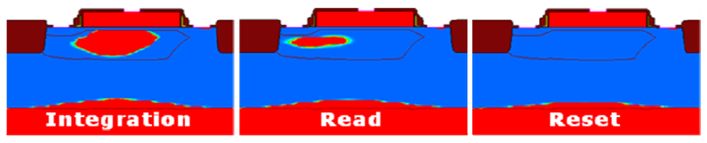
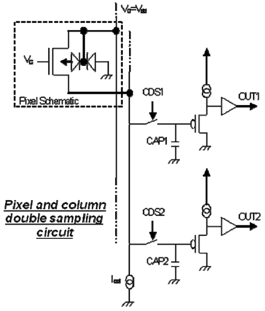
2. Pixel Structure and Operating Principle
3. Modeling and Model Validation
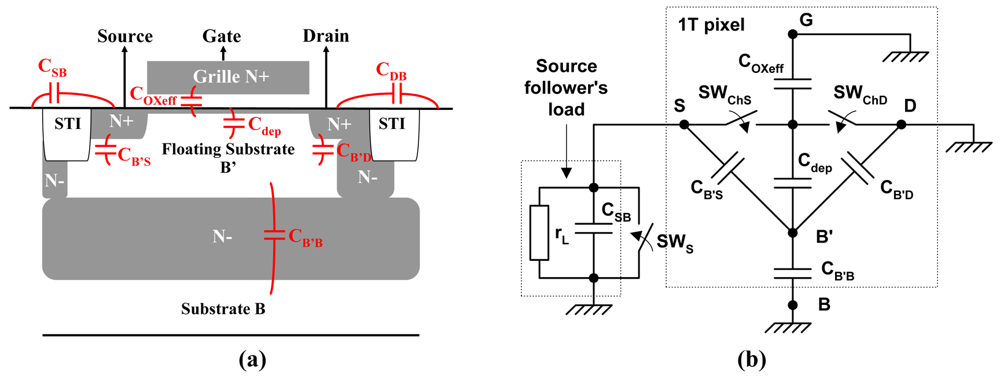
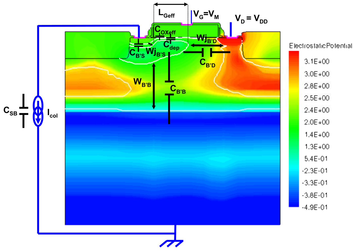
3.1. Model Description
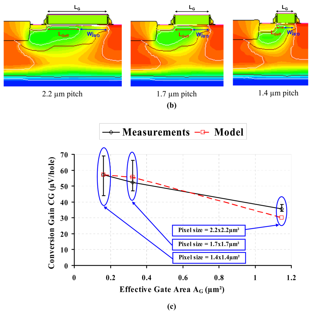
3.2. Extraction of Parameters
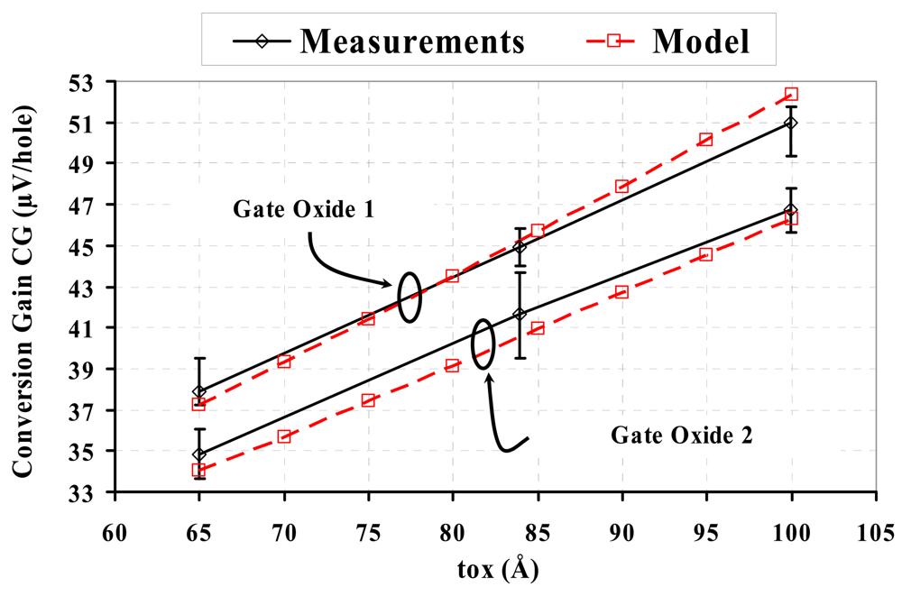
3.3. Model Validation
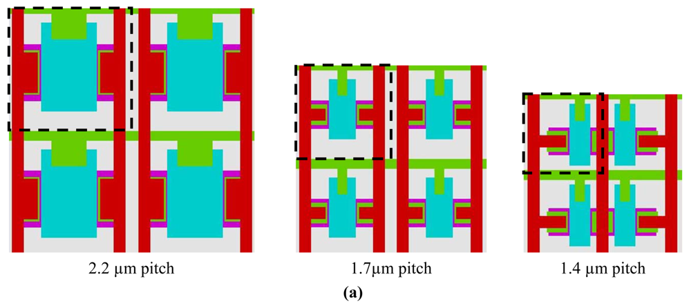
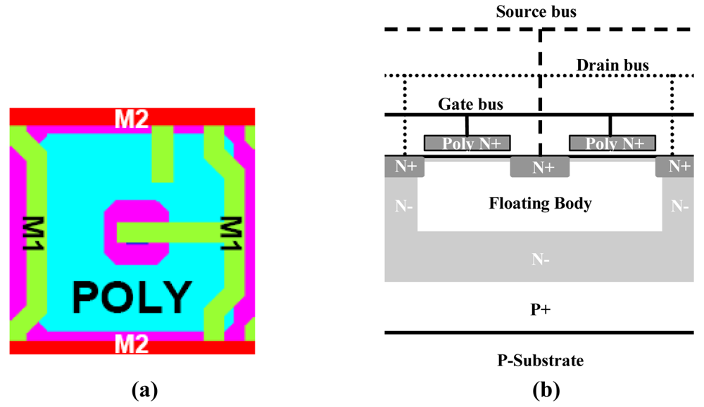
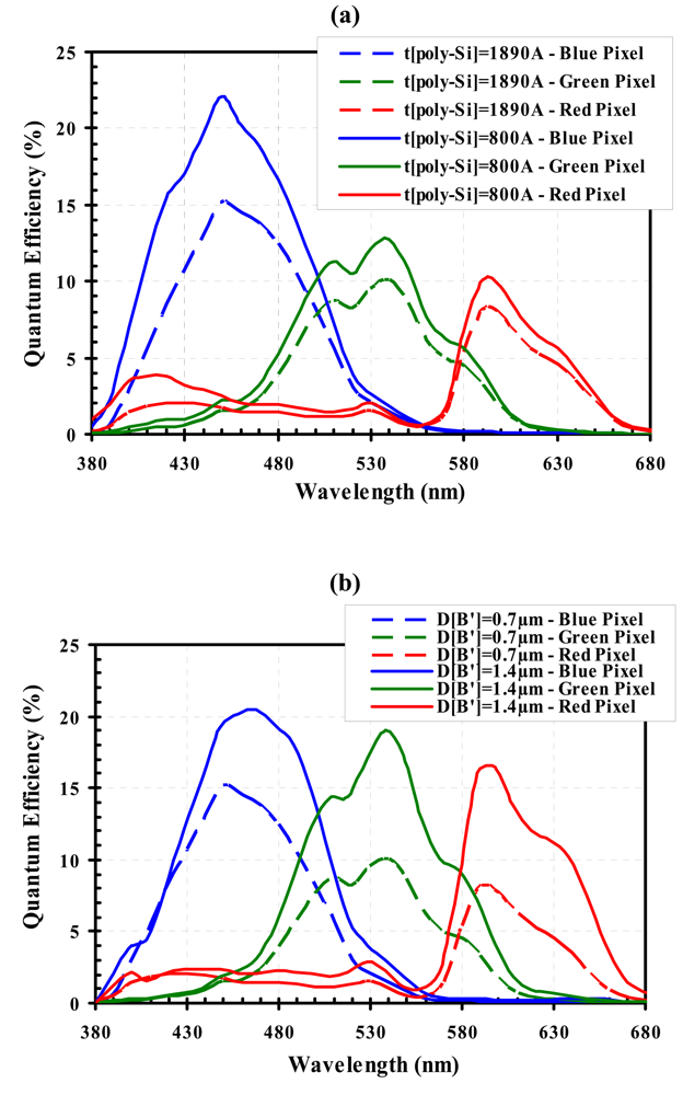
4. Implementation Configurations
- -
- increasing gate-oxide thickness to enhance CG;
- -
- gate oxidation with and without nitridation (gate oxide 1 and gate oxide 2) to choose one with better noise performance.
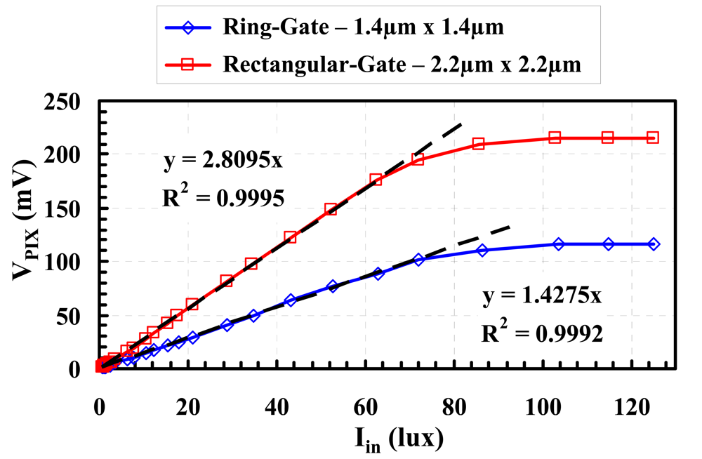
5. Pixel Characteristics
- -
- pixel shrink will lead to rapid degradation of sensitivity;
- -
- for a given pixel size the ring-gate configuration has better sensitivity than the rectangular-gate one.
- -
- smaller size for a comparable fill factor, mainly because STI is not employed;
- -
- larger CG, because of smaller size;
- -
- much lower dark current thanks to STI suppression, smooth-shape layout and smaller size;
- -
- lower temporal noise, partly because of CG improvement;
- -
- much lower Dark FPN (Fixed Pattern Noise, which may in large part be due to dark current), thanks to dark current reduction;
- -
- larger dynamic range, because improved signal-to-noise ratio outweighs FWC degradation.
- -
- lower FWC, because of smaller size and ring shape of the charge-storage region [19];
- -
- poorer sensitivity, due to size reduction.
6. Conclusions
Acknowledgments
References and Notes
- Agranov, G.; Gilton, T.; Mauritzson, R.; Boettiger, U.; Altice, P.; Shah, J.; Ladd, J.; Fan, X.; Brady, F.; McKee, J.; Hong, C.; Li, X.; Patrick, I. Optical-Electrical Characteristics of Small, Sub-4 μm and sub-3 μm Pixels for Modern CMOS Image Sensors. In Proc. IEEE Workshop on Charge-Coupled Devices and Advanced Image Sensors; Nagano, 2005; pp. 206–209. [Google Scholar]
- Lee, S.-H.; Moon, C.-R.; Paik, K.-H.; Hwang, S.-H.; Shin, J.-C.; Jung, J.; Lee, K.; Noh, H.; Lee, D.; Kim, K. The Features and Characteristics of 5M CMOS Image Sensor with Topologically Unique 1.7×1.7 μm² pixel. Symposium on VLSI Technology Dig. Tech. Papers, Honolulu; 2006. [Google Scholar]
- Cohen, M.; Roy, F.; Herault, D.; Cazaux, Y.; Gandolfi, A.; Reynard, J. P.; Cowache, C.; Bruno, E.; Girault, T.; Vaillant, J.; Barbier, F.; Sanchez, Y.; Hotellier, N.; LeBorgne, O.; Augier, C.; Inard, A.; Jagueneau, T.; Zinck, C.; Michailos, J.; Mazaleyrat, E. Fully Optimized Cu Based Process with Dedicated Cavity Etch for 1.75 μm and 1.45 μm Pixel Pitch CMOS Image Sensors. IEEE International Electron Devices Meeting (IEDM) Dig. Tech. Papers; San Francisco, 2006. [Google Scholar]
- Matsumoto, K.; Takayanagi, I.; Nakamura, T.; Ohta, R. The Operation Mechanism of a Charge Modulation Device (CMD) Image Sensor. IEEE Trans. Electron. Dev. 1991, 38, 989–998. [Google Scholar]
- Hynecek, J. BCMD - An Improved Photosite Structure for High-Density Image Sensors. IEEE Trans. Electron.Dev. 1991, 38, 1011–1020. [Google Scholar]
- Miida, T.; Kawajiri, K.; Terakago, H.; Endo, T.; Pkazaki, T.; Yamamoto, S.; Nishimura, A. A 1.5MPixel Imager with Localized Hole-Modulation Method. International Solid-State Circuits Conference (ISSCC) Dig. Tech. Papers, San Francisco; 2002; pp. 42–43. [Google Scholar]
- Sze, S. M. Physics of Semiconductor devices, 2nd Ed. ed; John Wiley & Sons: New York, 1981; pp. 457–462. [Google Scholar]
- Merckel, G. Contribution à L'Analyse Physique du Transistor MOS Dans Son Evolution Vers Les Microstructures. Thesis, INP, Grenoble, France, 1979. [Google Scholar]
- van Langevelde, R.; Gildenblat, G. PSP: An Advanced Surface-Potential-Based MOSFET Model. In Transistor level modelling for analog/RF IC design; Springer: Netherlands, 2006; Ch. 2; pp. 29–66. [Google Scholar]
- Leyris, C. Etude de Bruit Basse Fréquence de Type R.T.S. Dans Les Capteurs D'Images à Pixels Actifs CMOS. Thesis, CEM2, Montepellier, France, 2006. [Google Scholar]
- Leyris, C.; Martinez, F.; Hoffmann, A.; Valenza, M.; Vildeuil, J. C. N-MOSFET Oxide Trap Characterization Induced by Nitridation Process Using RTS Noise Analysis. Microelectron. Rel. 2007, 47, 41–45. [Google Scholar]
- Loukianova, N.V.; Folkerts, H. O.; Maas, J. P. V.; Verbugt, D. W. E.; Mierop, A. J.; Hoekstra, W.; Roks, E.; Theuwissen, A. J. P. Leakage Current Modeling of Test Structures for Characterization of Dark Current in CMOS Image Sensors. IEEE Trans. Electron. Dev. 2003, 50, 77–82. [Google Scholar]
- Machlup, S. Noise in Semiconductors: Spectrum of a Two Parameter Random Signal. J. Appl. Phys. 1954, 25, 341–343. [Google Scholar]
- Hooge, F. N. 1/f noise sources. IEEE Trans. Electron. Dev. 1994, 41, 1926–1935. [Google Scholar]
- Vandamme, E. P.; Vandamme, L. K. J. Critical Discussion on Unified 1/f Noise Models for MOSFETs. IEEE Trans. Electron. Dev. 2000, 47, 2146–2152. [Google Scholar]
- Leyris, C.; Roy, F.; Marin, M. Modeling of the Temporal Pixel to Pixel Noise of CMOS Image Sensors. In 2007 International Image Sensor Workshop (IISW-2007); Ogunquit, Maine, USA, 2007; pp. 219–222. [Google Scholar]
- Tournier, A.; Lu, G.-N.; Roy, F.; Deschamps, B. A 2.2μm-Pitch Single-Transistor Charge-Modulation Pixel in a 0.13μm CMOS Process. IEEE Trans. Electron. Dev. 2007, 54, 2623–2629. [Google Scholar]
- Tournier, A.; Roy, F.; Lu, G.-N.; Deschamps, B. Improved Design of 1T Charge-Modulation Pixel Structure for Small-Size and Low-Dark-Current Achievements. In 2007 International Image Sensor Workshop (IISW-2007); Ogunquit, Maine, USA, 2007; pp. 315–318. [Google Scholar]
- Tournier, A.; Roy, F.; Lu, G.-N.; Deschamps, B. 1.4-μm-Pitch 50% Fill-Factor 1T Charge-Modulation Pixel for CMOS Image Sensors. IEEE Electron. Dev. Lett. 2008, 29, 221–223. [Google Scholar]


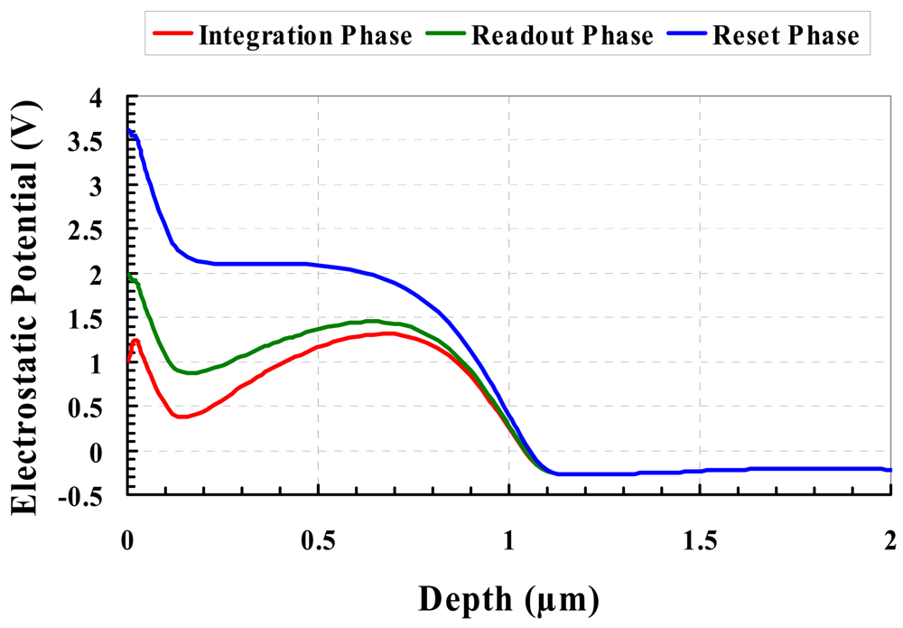
| VD | VG | VS | |
|---|---|---|---|
| Integration Readout | 3.3 V | ∼ 0 V | 3.3 V |
| 3.3 V | ∼ 2 V | Connection to load | |
| Reset | 3.3 V | 3.3 V | 3.3 V |
| Parameter | Expression | Value |
| AG | 0.62 μm2 | |
| COXeff | 3.28 fF | |
| Cdep | 1.82 fF | |
| CB'D | 0.019 fF | |
| CB'S | 0.60 fF | |
| CB'B | 0.081 fF | |
| CB' | 2.52 fF |
| tox | 65 Å | 84 Å | 100 Å |
|---|---|---|---|
| Ox + Ni (gate oxide 1) | 5.1 h+ | 4.9 h+ | 4.8 h+ |
| Ox only (gate oxide 2) | 4.5 h+ | 4.1 h+ | 4.0 h+ |
| Pixel size (μm2) | Fill factor | Sensitivity (h+/lux.s) | |
|---|---|---|---|
| Rectangular-gate | 2.2 × 2.2 = 4.84 | 46% | 1840 |
| Rectangular-gate | 1.7 × 1.7 = 2.89 | 40% | 550 |
| Rectangular-gate | 1.4 × 1.4 = 1.96 | 34% | 290 |
| Ring-gate | 1.4 × 1.4 = 1.96 | 50% | 590 |
| Parameter | 2.2μm-pitch rectangular-gate | 1.4μm-pitch ring-gate | Testing conditions |
|---|---|---|---|
| Process | 0.13 μm 1 P 4 M CMOS | 0.13 μm FE + 90 nm BE 1P 3M CMOS | |
| Test chip size | 3.2 mm × 3.2 mm | 3.0 mm × 3.2 mm | |
| Pixel size | 2.2 μm × 2.2 μm | 1.4 μm × 1.4 μm | |
| Number of Pixels | CIF (352 × 288) | VGA (672 × 512) | |
| Fill factor | 46 % | 50 % | Without microlens |
| Supply voltage | 1.2 V / 3.3V | 1.2 V / 3.3 V | |
| Conversion gain | 35 μV/h+ | 58 μV/h+ | |
| Full well capacity | 6200 h+ | 2000 h+ | |
| Dark current | 500 h+/s | 39.7 h+/s | Mean value @ RT |
| Pixel temporal Noise | 6 h+ | 2.4 h+ | In darkness |
| Pixel Dark FPN | 39.5 h+ | 4.3 h+ | Without additional correction circuit |
| Noise floor | 40 h+ | 4.9 h+ | Temporal noise, FPN & DSNU in darkness |
| Dynamic range | 44 dB | 52 dB | Usable Well over Noise floor |
| Sensitivity | 1840 h+/lux.s | 590 h+/lux.s | B/W sensitivity without microlens Halogen 3200 K IR cut off 650 nm |
© 2009 by the authors; licensee Molecular Diversity Preservation International, Basel, Switzerland. This article is an open access article distributed under the terms and conditions of the Creative Commons Attribution license (http://creativecommons.org/licenses/by/3.0/).
Share and Cite
Lu, G.-N.; Tournier, A.; Roy, F.; Deschamps, B. 1T Pixel Using Floating-Body MOSFET for CMOS Image Sensors. Sensors 2009, 9, 131-147. https://doi.org/10.3390/s90100131
Lu G-N, Tournier A, Roy F, Deschamps B. 1T Pixel Using Floating-Body MOSFET for CMOS Image Sensors. Sensors. 2009; 9(1):131-147. https://doi.org/10.3390/s90100131
Chicago/Turabian StyleLu, Guo-Neng, Arnaud Tournier, François Roy, and Benoît Deschamps. 2009. "1T Pixel Using Floating-Body MOSFET for CMOS Image Sensors" Sensors 9, no. 1: 131-147. https://doi.org/10.3390/s90100131