Article

Integrated Inductors for RF Transmitters in CMOS/MEMS Smart Microsensor Systems

1
Department of Electrical and Electronic Engineering ,Toyohashi University of Technology, Toyohashi/Aichi, 441-8580, Japan
2
Intelligent Sensing System Research Center, Toyohashi University of Technology, Toyohashi/Aichi, 441-8580, Japan
3
JST-CREST, Japan Science and Technology Agency
*
Author to whom correspondence should be addressed.
Sensors 2007, 7(8), 1387-1398; https://doi.org/10.3390/s7081387
Submission received: 21 June 2007 / Accepted: 30 July 2007 / Published: 31 July 2007
(This article belongs to the Special Issue Modeling, Testing and Reliability Issues in MEMS Engineering)

Abstract

:
This paper presents the integration of an inductor by complementary metal-oxide-semiconductor (CMOS) compatible processes for integrated smart microsensor systems that have been developed to monitor the motion and vital signs of humans in various environments. Integration of radio frequency transmitter (RF) technology with complementary metal-oxide-semiconductor/micro electro mechanical systems (CMOS/MEMS) microsensors is required to realize the wireless smart microsensors system. The essential RF components such as a voltage controlled RF-CMOS oscillator (VCO), spiral inductors for an LC resonator and an integrated antenna have been fabricated and evaluated experimentally. The fabricated RF transmitter and integrated antenna were packaged with subminiature series A (SMA) connectors, respectively. For the impedance (50 Ω) matching, a bonding wire type inductor was developed. In this paper, the design and fabrication of the bonding wire inductor for impedance matching is described. Integrated techniques for the RF transmitter by CMOS compatible processes have been successfully developed. After matching by inserting the bonding wire inductor between the on-chip integrated antenna and the VCO output, the measured emission power at distance of 5 m from RF transmitter was -37 dBm (0.2 μW).

1. Introduction

Intelligent human sensing systems and wearable medical monitoring and alert systems have been proposed not only for high-risk and chronically ill patients, but also for other healthcare field applications. Life Shirt [1] and Sense Wear [2] use this basic concept of wearable sensor systems. However, further miniaturization of each sensing device is necessary for a wearable sensor system to be unobtrusively attached to the body. One of the objectives of our research work is the realization of wireless smart microsensor systems developed to monitor the activity and multiple vital signs of humans in various environments. The concept of our smart microsensor systems has been reported in our previous work [3].
Figure 1 shows the diagram of the proposed concept of our intelligent human sensing system [3]. The system can collect data during the subject's daily routine, providing health information in real-time to medical researchers. To meet this objective this system should be a wearable, mobile, and fully integrated wireless sensor system. Wearable sensing systems and smart sensors that are integrated with the communication circuit have been reported. For example, the Wearable Computing Group's LiveNet [4] of MIT and the Smart Dust Project [5] of the University of California, Berkeley, are pioneering works in this field. However, device fabrication technology needed to achieve integration of various sensors and the RF transmitter, including complementary metal-oxide semiconductor (CMOS) processing circuits on silicon, has not been established at present. Figures 2(a) and (b) show a CMOS-integrated three axis accelerometer [6] and a smart nerve potential sensor array [7], respectively, that have been developed by our group. They will be the essential sensor elements for detection of human motion and nerve activity for the purpose of intelligent human sensing. The integration of the RF communication unit, including RF circuitry, and the on-chip antenna on such smart complementary metal oxide-semiconductor/micro electro mechanical systems (CMOS/MEMS) sensors is required. Thus, essential fabrication technologies of the RF communication unit for wireless smart micro sensors have been developed [8]. Nevertheless, the passive matching element that is inductor was not yet integrated. In this paper, the development of an integration technique for RF transmitters to include an integrated inductor that will be integrated on smart microsensors is presented.

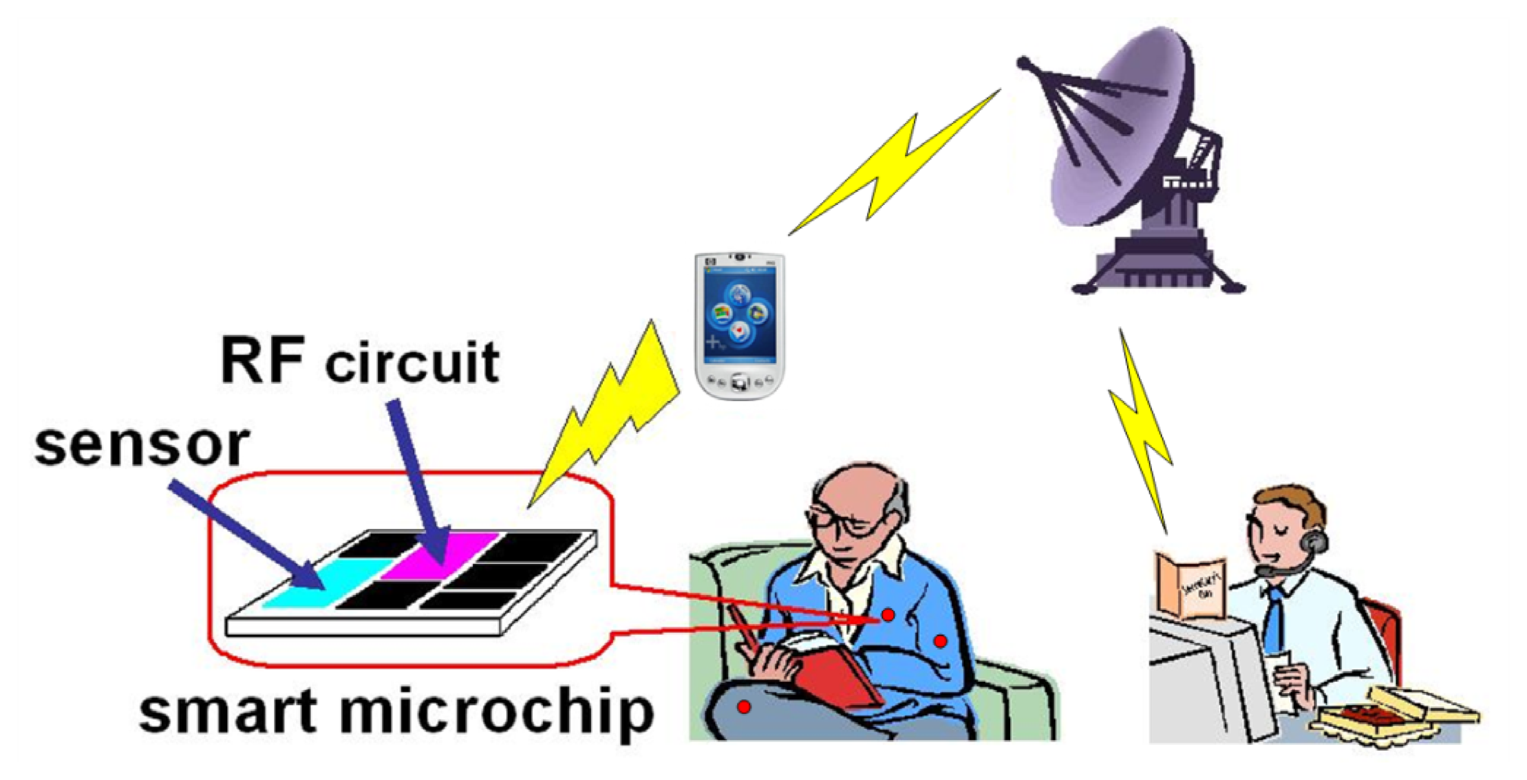
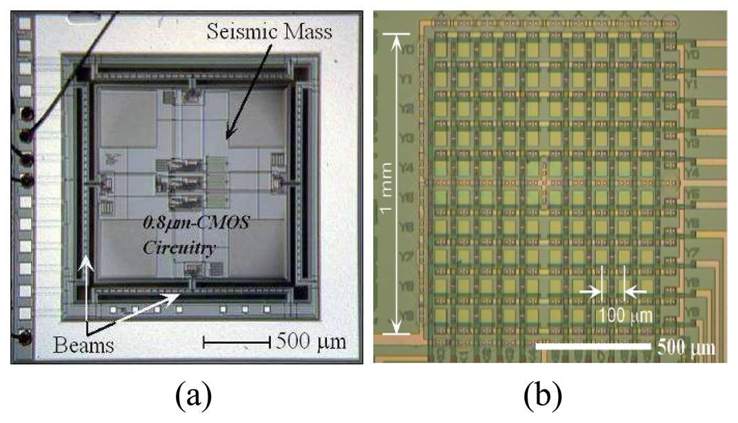
2. Smart microsensors for Intelligent Human Sensing System

The introduction of wireless communication is essential to enhance the application of smart sensors. In the case in which each smart sensor adopts independent communication methods, the problem is that the sensors will have to be made larger and will consume correspondingly increased power. Additionally, in order to measure the motion and vital signs of humans accurately, each sensor must be attached to the appropriate part of the human body for effective sensing. In some cases, multimodal smart sensors with many types of integrated sensors will be considered, where each sensor is completely integrated with minimal control and communication circuits in order to achieve the smallest and most easily attachable form. Integrated MEMS sensors with CMOS technology, RF circuits and small-sized microchip of fully integrated wireless smart microsensors will be realized in the near future. In order to communicate with each smart sensor at the front end of a network, a short-distance (∼1m) wireless communication is used. This short-distance network uses an extremely low power radio transmitter and has been designed to satisfy the legal limit for no licensed transmitters in Japan, which is below 500μV/m electric field at 3-m distance for under the 322-MHz band.
Figure 3 shows the configuration of a simple RF transmitter for monolithic integration with CMOS/MEMS smart sensors [8]. The transmitter can be realized by standard CMOS technology, and it is integrated with CMOS/MEMS sensors. It consists of a signal conditioner, a modulator, an output amplifier, and an on-chip integrated antenna. A voltage controlled RF-CMOS oscillator (VCO) is a key building block in wireless transceivers and other communication systems. The ring oscillator is one of the most popular wide-tuning-range topologies, and can be used as a VCO or a phase locked loop (PLL) with the bias controllability of the inverters. In this study, the VCO controlled by the sensor signal is used as a direct FM modulator, which is considered the simplest integrated transmitter. Therefore, in this study the VCO functions as the carrier generator, modulator, and power amplifier. Also, an LC resonator is used as an integrated antenna. A 300-MHz CMOS VCO was designed and fabricated by 2.5 μm CMOS technology at the Toyohashi University of Technology. The key components, integrated LC resonators and the antenna element were also integrated on the chip. They were realized by the aluminum metallization process at the end of the CMOS fabrication step, and could thus be integrated with the VCO. Their integration on CMOS/MEMS smart sensors is essential to realize monolithic wireless smart microsensors.

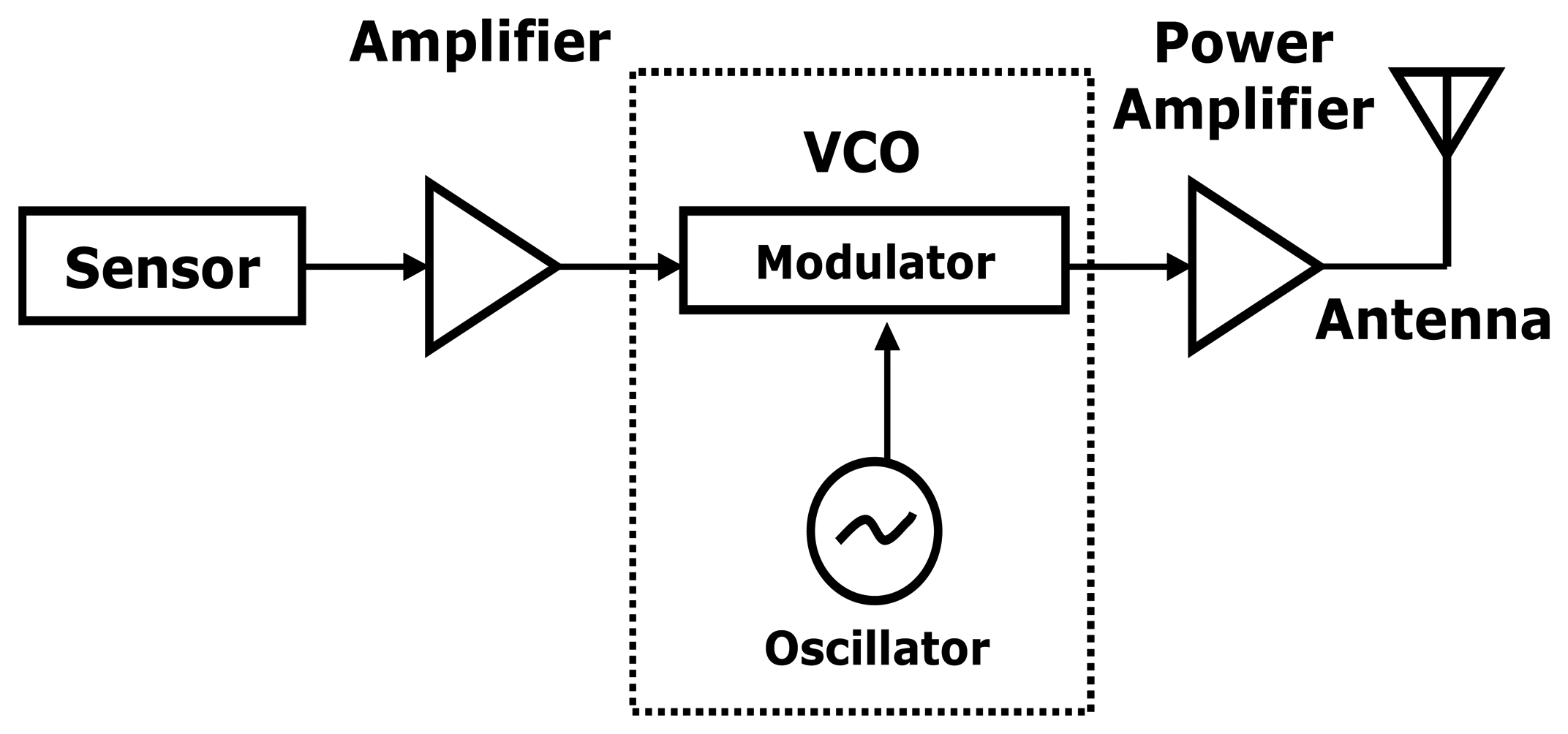
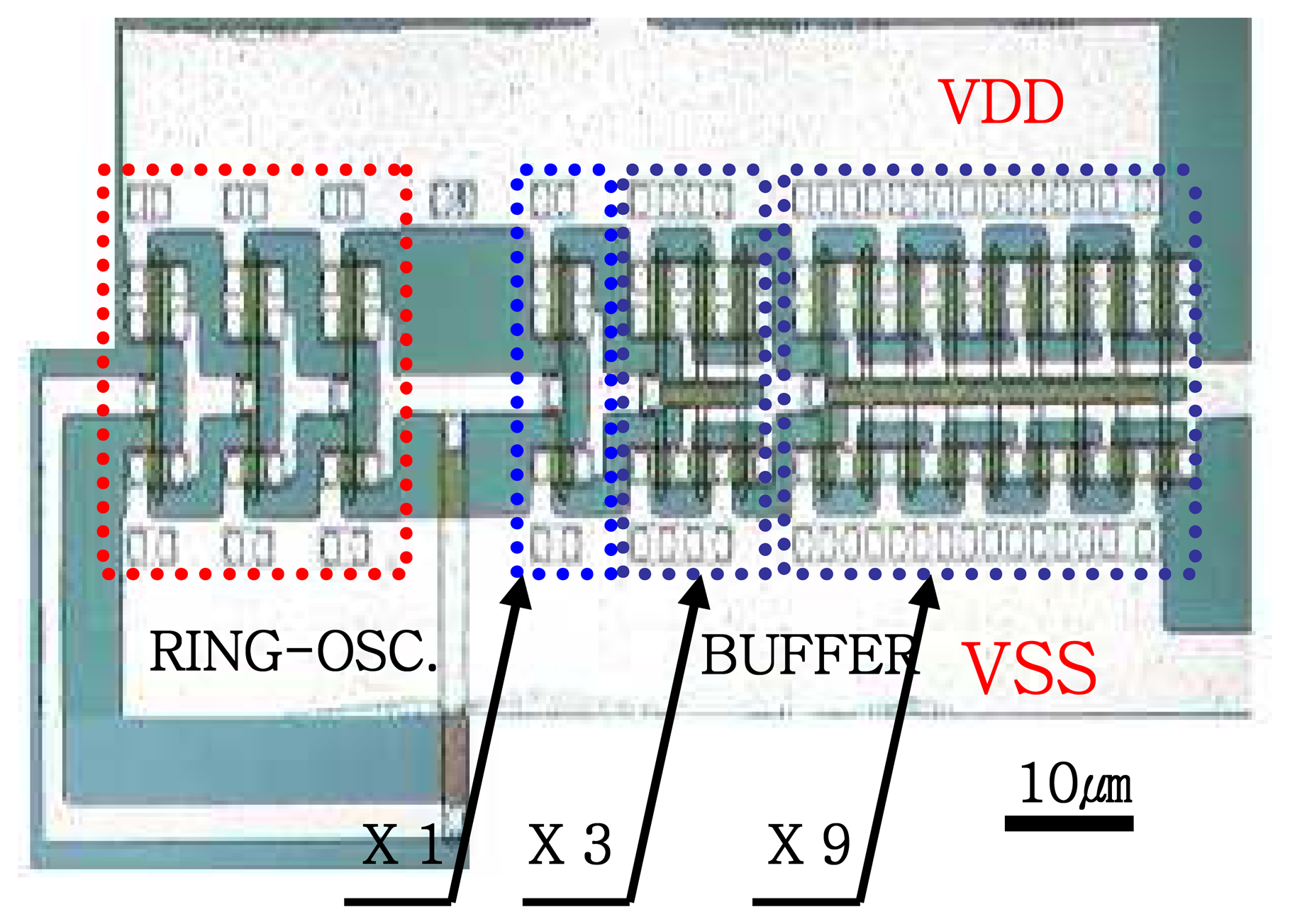
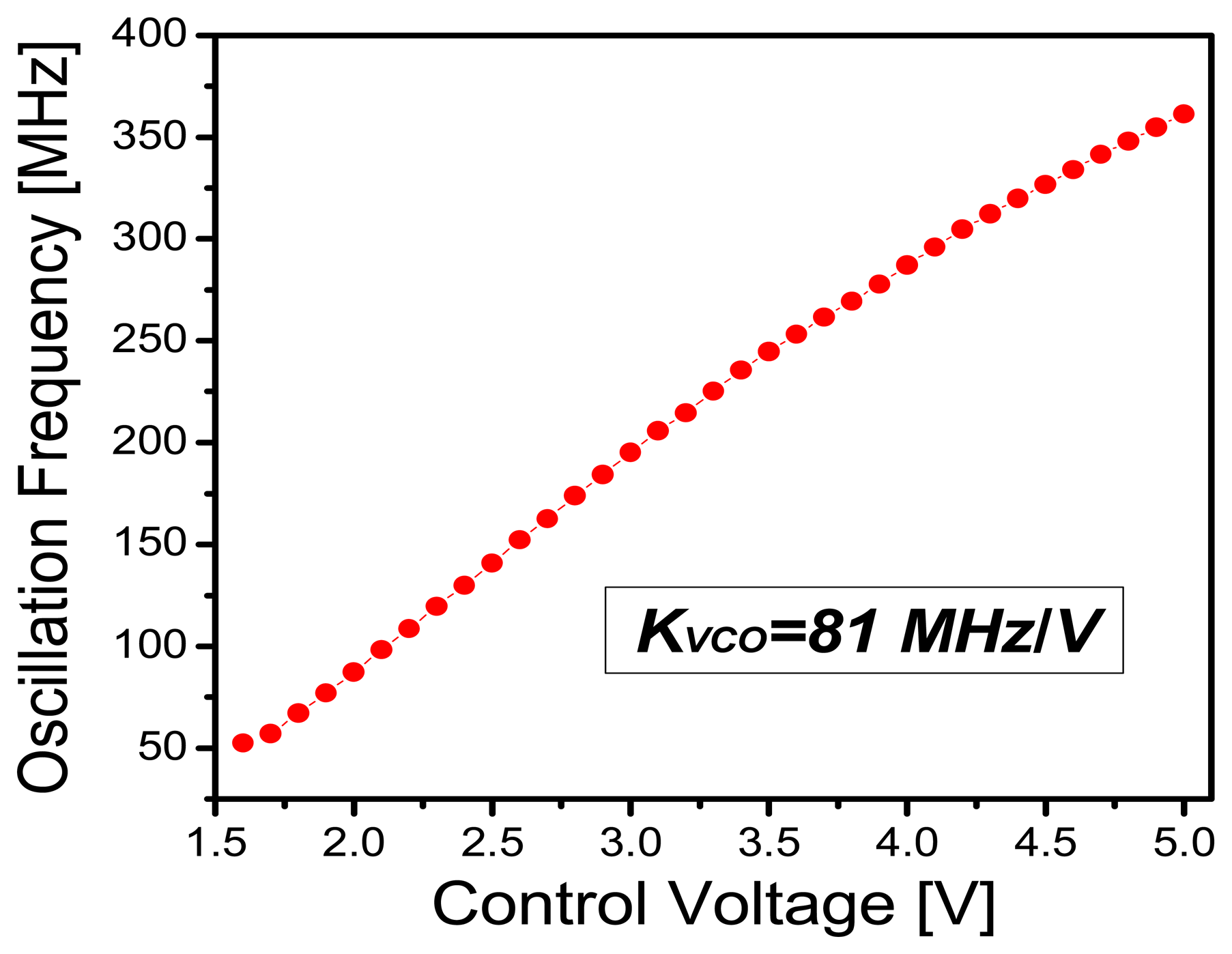
2.1. Integrated 300-MHz CMOS VCOs

High frequency oscillators have been designed and fabricated by reducing the size of CMOS design rules according to the CMOS scaling law [9]. Figure 4 shows a photograph of a fabricated CMOS VCO that was used as the FM transmitter in the smart microsensor by our previews works [8]. It consists of three-stage inverters and a power amplifier with 1-, 3-, and 9-times buffer stages. The supply voltage of the VCO was used to control the oscillation frequency in this study. The fabricated CMOS VCOs were evaluated. The measured fundamental frequency of the oscillation output of the CMOS VCO was 351 MHz in this measurement. The obtained output power for a 50Ω load was -0.93 dBm (about 810μW). The targeted center frequency of the VCO was 300-MHz. Figure 5 shows the measured relationship between the oscillation frequency and the control voltage of the fabricated VCO. A wide range of frequency control was realized from 52.4- to 361.3-MHz for 1.6- to 5-V control voltage, respectively. The measured coefficient of VCO sensitivity to voltage (Kvco) extracted from the relationship in Figure 5 was about 81-MHz/V at 25 °C. The oscillation frequency was matched with the targeted center frequency of 300-MHz at 4.1 V. This sensitivity was high enough for our application.

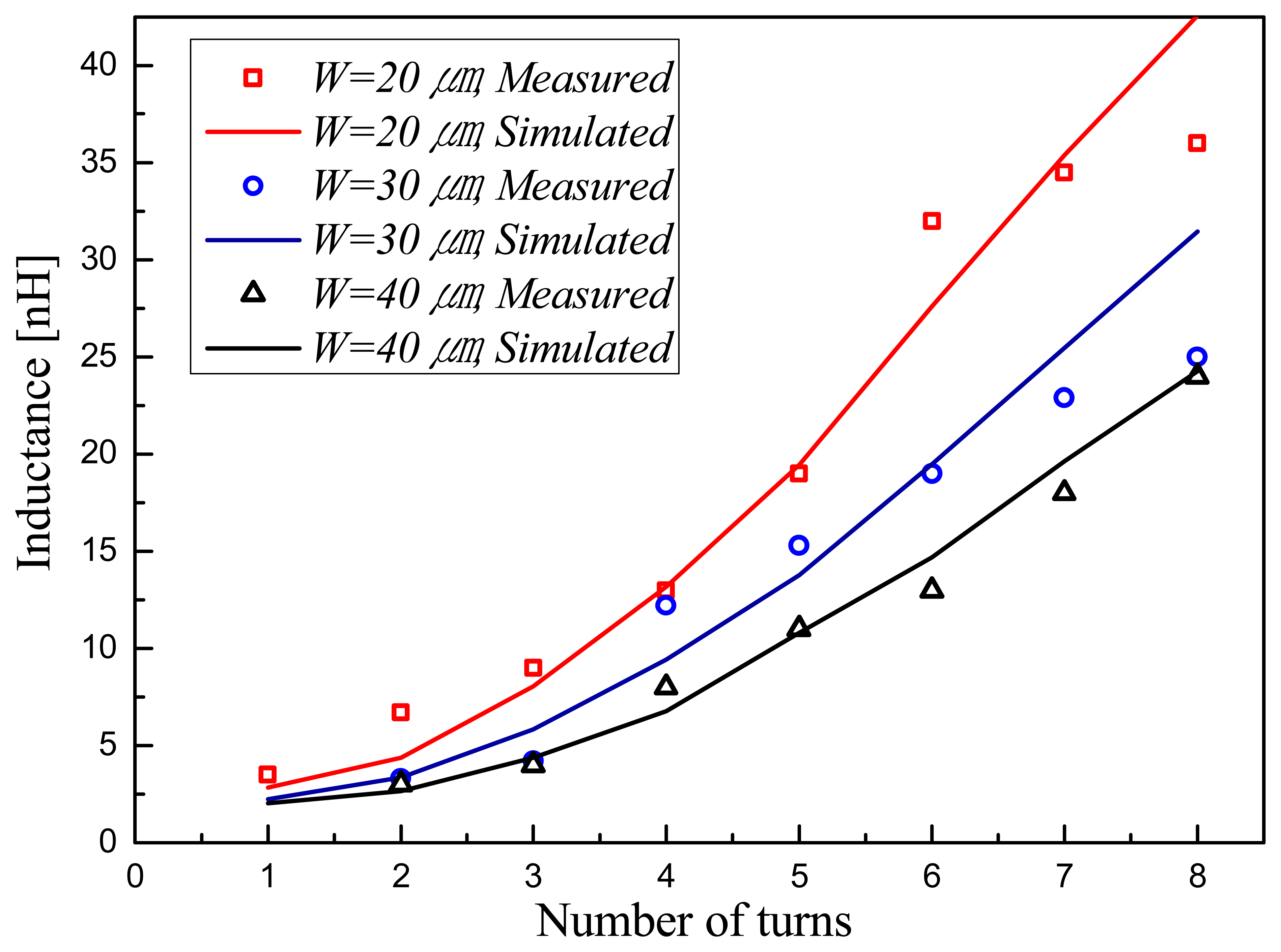
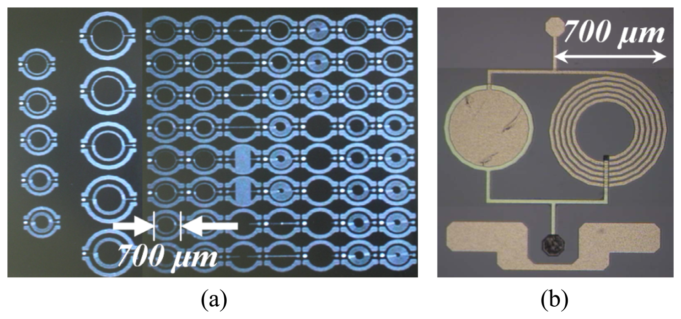
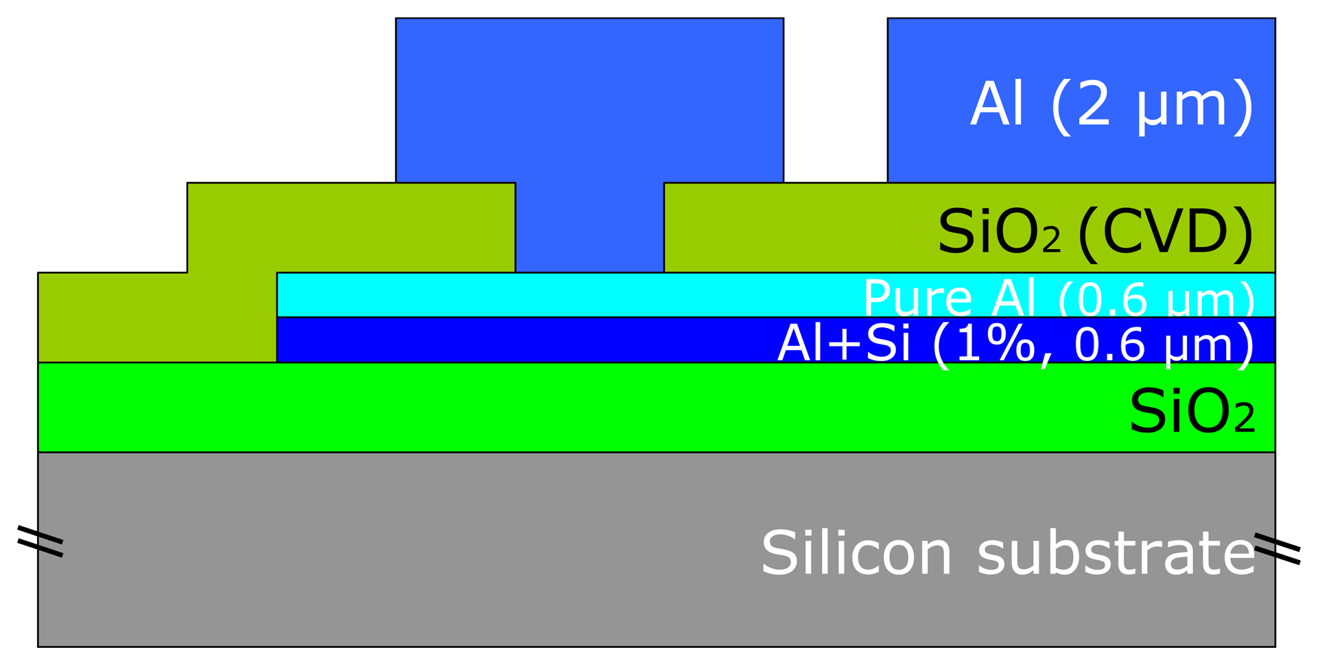
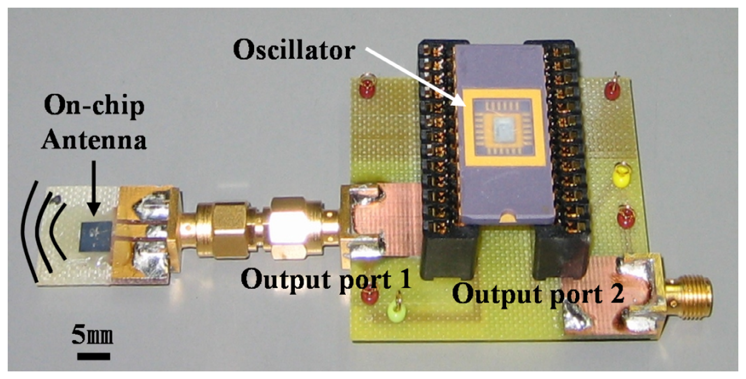
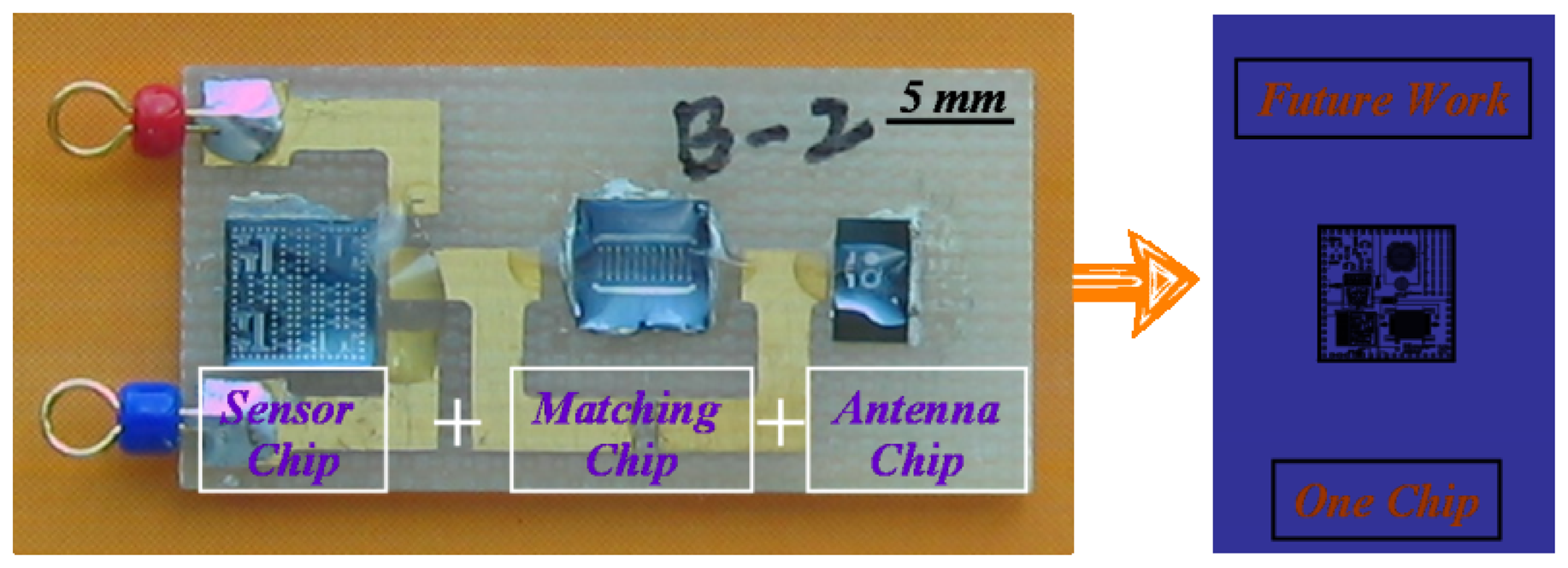
2.2. Integrated LC resonator and integrated antenna

A LC resonator and an integrated antenna in the 300-MHz range were designed and fabricated. Some types of patterns were designed and fabricated using two metal (aluminum) layers. The patterns of spiral inductors and LC resonator were selected and optimized from various geometric parameters.
When the number of sides grows (square to circular geometry) the inductance grows faster than the resistance. It can be set as a design rule that an optimum inductor has to be designed with the highest number of sides allowed by the fabrication technology [10]. On the other hand, if the spacing is reduced, the quality to augment because the resistance is maintained and the inductance is increased be set as a design rule that to maximize the quality of an inductor has to be designed with smallest spacing allowed by the technology. The external radius and number of turns have been analyzed. They define the inductor's length. Figure 6 shows the influence of the number of turns comparing the measured results with simulated results. As the number of turns increases the inductance grows and the quality curve shifts to lower frequencies. However, an empirical analysis to set the design rule for the external radius and the number of turns is necessary. Figure 6 shows also the influence of the track widths. The track widths increase the inductance to diminution because more metal track length would be needed leading probably to higher DC resistance and coupling to the substrate [11].
Figure 7 shows the fabricated coils and LC resonator integrated on silicon for the 300-MHz frequency band. Figure 7(a) shows the fabricated integrated inductors with various layout patterns. Finally, the pattern of the inductor was optimized and used in the LC resonator, as shown in Figure 7(b). All the materials are common to standard CMOS fabrication technologies. The cross-sectional structure of the spiral inductors is shown in Figure 8. A thick (2μm) second metal layer was formed to obtain a lower resistive conductor because the resistance of the conductor degrades the Q-factor of integrated RF components, as is well known [12]. As shown in the figure, the first metal layer has two layers of 1% silicon composite aluminum and pure aluminum. The lower layer is necessary to prevent harmful reactions between the first metal layer and silicon device surface, while the upper layer is required for better contact with the second metal layer (pure aluminum). The parameters of spiral inductors are the number of sides, the space between tracks, the number of turns, the external radius, and the track widths. The performance of the spiral inductor has been satisfactory for this application of design improvement. Nevertheless, parameter extraction and further optimization will be continued to obtain higher performance. The spiral inductor was designed with the modified wideband π model [13]. An inductance of 28.1nH and a Q-factor of over 1 were the design targets. First, the fabricated spiral inductors and LC resonators were evaluated at the wafer level by RF probes for electrical checks. Then they are mounted on packages (test fixture). A Subminiature series A (SMA) connector was used between the devices under test (DUT) and the VNA. The measured Q-factor of the inductor was 0.22 at 300-MHz. The low Q-factor is due to parasitic effects such as magnetic field penetration, metal–substrate capacitance, and so on. The measured resonant frequency was about 600-MHz. When an inductor is integrated on silicon, some undesirable induced effects show up. The reason is that the metallic layers are separated from the semiconductor substrate by a layer of silicon dioxide. These effects can be classified in two types, magnetically induced [13] and electrically induced [14]. Because of the induced effects, the value of inductance will decrease and the resonant frequency becomes higher. The parasitic effect also causes impedance mismatching at the targeted carrier frequency (300-MHz in this study). Thus, an impedance matching procedure is necessary to obtain better performance of the integrated LC resonator used as an on-chip antenna for RF radiation. Improvement of the performance of the LC resonator is discussed in the next section in detail.

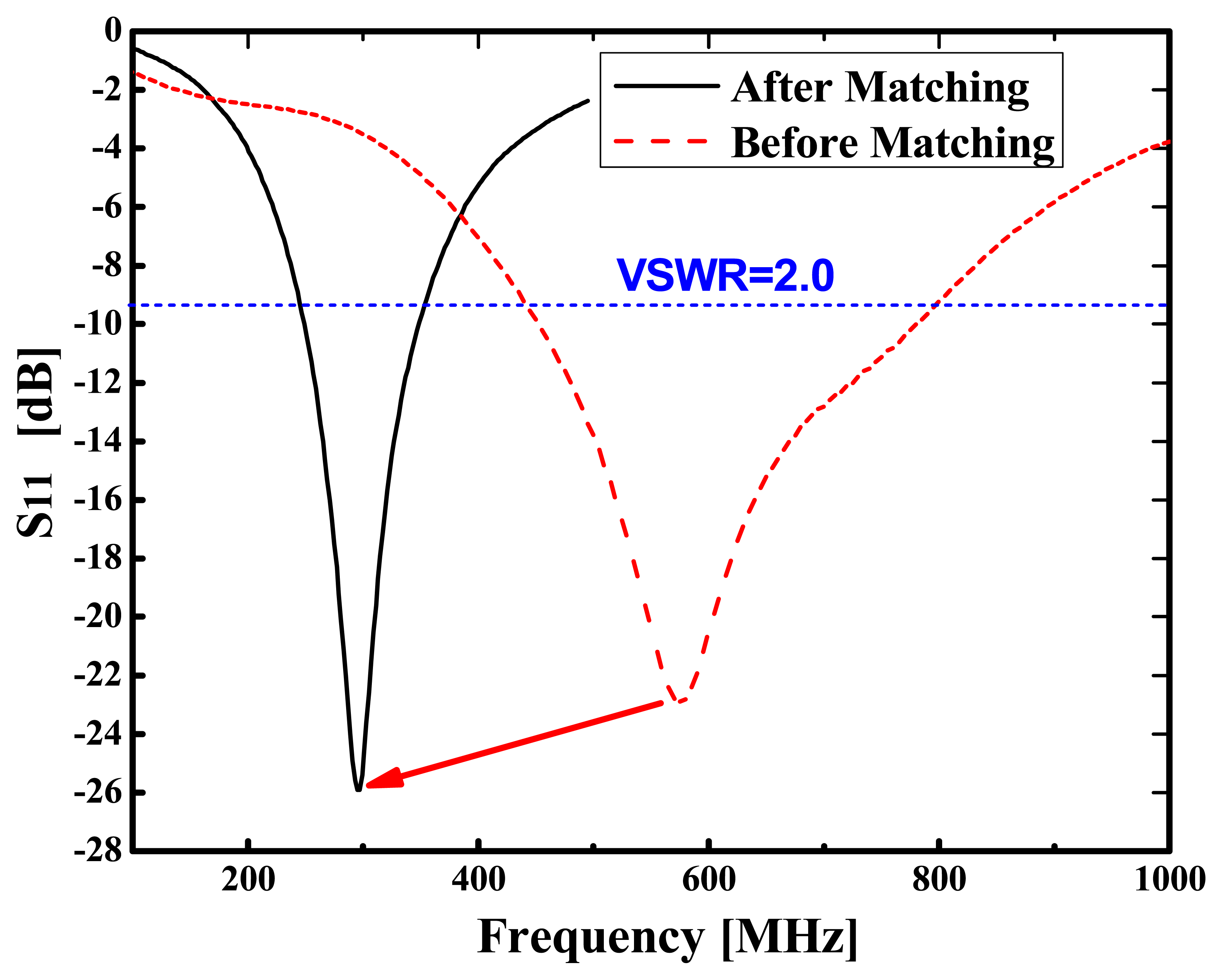
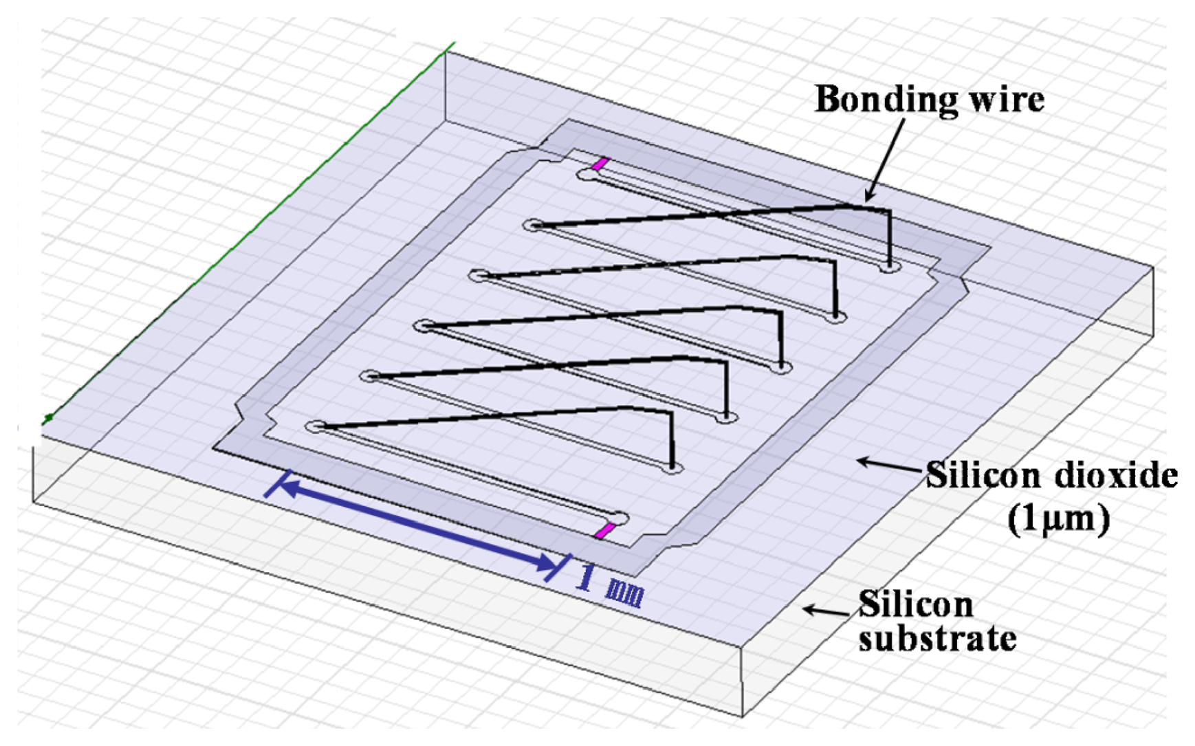
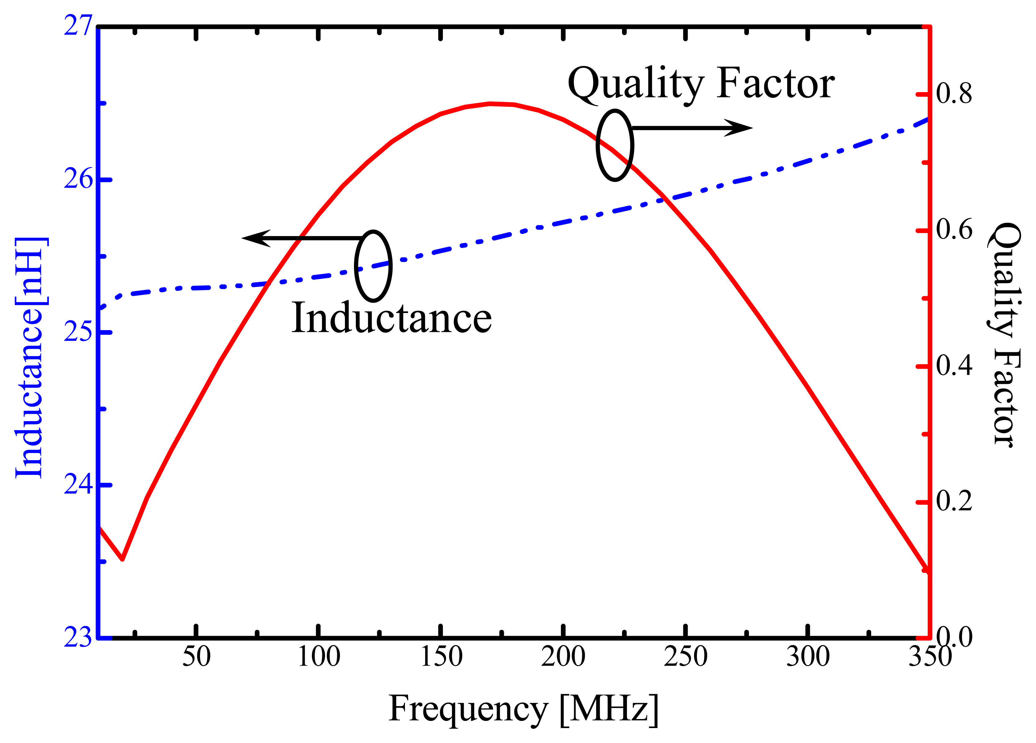
3. Impedance matching procedure and the bonding wire inductor

The CMOS VCOs and integrated antennas were fabricated by the same CMOS technology on each silicon wafer. The fabricated CMOS VCOs and integrated antennas were packaged with the SMA connector for electrical connection. Before the impedance matching procedure, the output power of the CMOS VCO for 50Ω load was −0.93 dBm (=810 μW).
The output impedance of CMOS VCO has been well matched to 50Ω by inserting a passive matching element (series L, 27 nH). After the matching, the output power of the CMOS VCO became 1.09 dBm (=1.28 mW) at the same supply power. The power efficiency has become 50 % higher as compared to that before the matching. Although the matching was performed by a discrete component in this experiment, it is possible to be integrated on the same chip by extracting the proper value of the parameter from the experiment. Figure 9 shows the measured return loss characteristics before and after the impedance matching of the on-chip antenna fabricated on silicon. The center frequency was moved from 600-MHz to 300-MHz as a result of impedance matching. Also, the voltage standing wave ratio (VSWR) is improved by the matching procedure. The measured bandwidth with a VSWR better than 2.0 was approximately 247-to 351-MHz. This corresponds to the measured result of Figure 9.
Finally, the CMOS VCO and the on-chip antenna were combined to evaluate the performance of the RF transmission ability. The configuration of the measurement system for the transmission characteristic is shown in Figure 10. The packaged antenna on the silicon chip and the CMOS VCO chip were attached to SMA connectors for transmission characteristic measurement [8]. Each measurement commenced by sending out the signal generated from the CMOS VCO via the antenna on silicon. The signals received by a dipole antenna (Anritsu MP534A) were analyzed with a spectrum analyzer (HP8590D). For comparison, the transmission performance was measured before and after the impedance matching procedure discussed above. The received power of the dipole antenna was −44 dBm (39 nW) at a distance of 3-cm before the impedance matching procedure. This level of signal is too small to communicate the microsensor signal to the network. After that, the impedance matching circuit was inserted between the VCO and the on-chip antenna. Therefore, the VCO output, more than 5 m transmission of the RF signal from the microchip could be obtained with the dipole receiver antenna. Therefore, the measured emission power at distance of 5 m from RF transmitter was -37 dBm (0.2 μW) This electric field is high enough for our application of short-distance RF communication, and a ‘detuning’ of the impedance at 300-MHz was required for the legal limitation. The transmission characteristic of 300-MHz radiowave was much improved by the matching procedures of the impedance of the final output node of the CMOS circuit and the input impedance of the on-chip antenna.

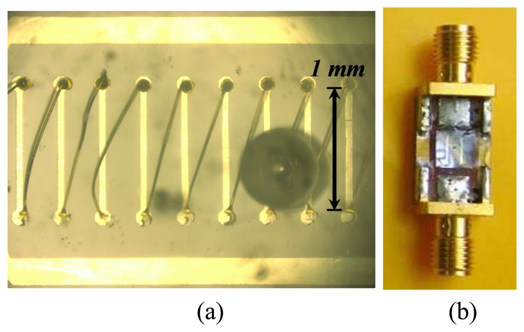
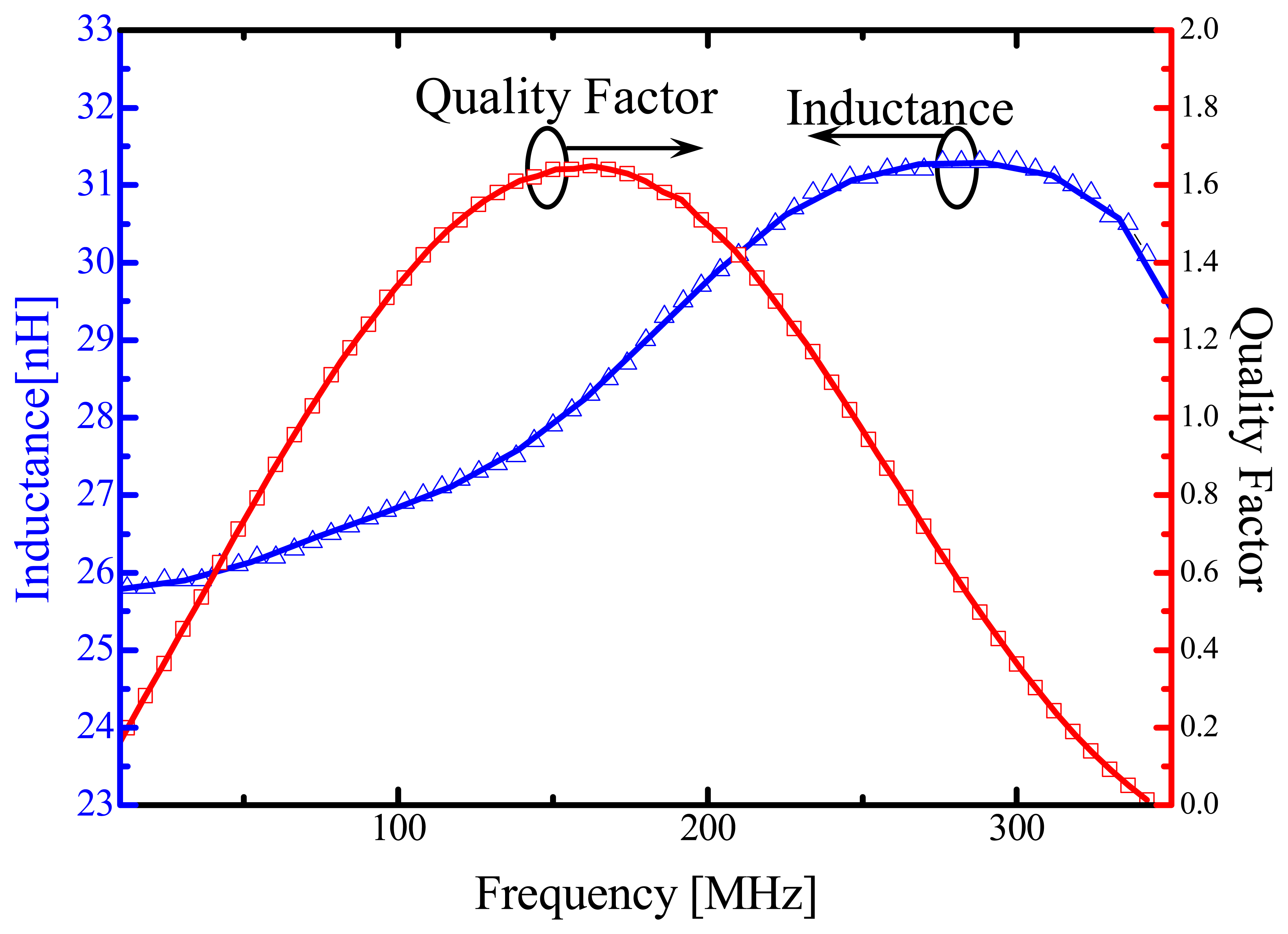
Bonding wire inductor for impedance matching

The Q-factor of an inductor is determined by its geometry and fabrication processes [15]. In our CMOS technologies, the Q-factor of a spiral inductor has been limited to 0.22 on 27 nH at 300-MHz band. Recently, inductor designs on CMOS and silicon-germanium (SiGe) substrates have resulted in a Q-factor of spiral inductors with typical inductance L of a few nH is over 12 at 2-GHz range. However in standard CMOS technologies, the Q-factor has been still less than 10, besides, the targeted inductance L in this study is around 27nH at 300-MHz band. The Q-factor of an inductor is in proportion to the operation frequency (ω) and inversely proportional to the resistance R. Therefore, low Q-factor of both spiral and bonding wire inductor is expected for our purpose. In the fabrication processes of CMOS/MEMS sensors, the inductor is fabricated by standard CMOS processes for compatibility with fabrication. If thick metal process can be utilized in CMOS fabrication process as an optional step, the Q-factor of an inductor will be improved by the low resistance of the metallic layers.
In this paper, the bonding wire inductors for impedance matching that will be integrated on the wireless smart microsensors have been developed. Figure 11 shows the simulation model of bonding wire inductor for Ansoft HFSS. The bonding wire inductor usually had known high Q inductor on silicon substrate.
Figure 12 presents the simulated Q and L of a bonding wire inductor at different frequencies. The resonant frequency is 370-MHz and L=26.1 nH at 300-MHz and Q of 0.79 at 170-MHz. The fabricated bonding wire inductor and the DUT for network analyzing are shown in Figure 13.
The bonding wire inductor results in Q of 1.65 at 162-MHz was measured. The resonant frequency is 345-MHz and L=31.3 nH at 300-MHz. The measured resonant frequency and inductance corresponded to the simulated results proportionally. However, the measured Q-factor did not correspond to the simulation. The Q-factor is dominated by the geometrics and process parameters of the inductor. Then, extraction of Q-factor from simulations is more complicated than the inductance. As a result, the Q-factor of bonding wire inductors was improved, then the Q-factor of spiral inductors and the bonding wire inductor was suitable for impedance matching. The measured results are shown in Figure 14. Therefore, the bonding wire inductors were fabricated and connected by wire bonding between the RF transmitter and the antenna.
The sensor chip consists of the RF transmitter chip and the bonding wire inductor chip for impedance matching and integrated antenna chip was fabricated on silicon, respectively. Following the fabricating, each chip was packaged on the printed circuit board (PCB). The transmission performance was measured after the impedance matching procedure using the wire bonding inductor. The received power really makes no difference between matching by the SMD inductor and the wire bonding inductor. Figure 15 presents the fabricated smart microsensor on the PCB and the concept of one chip for the further works. The integration techniques for fully integrated smart microsensor were successfully established. By these integration techniques, the wireless smart microsensor system that was fully integrated one chip shown in the Figure 15 will be realized in our next work.

4. Conclusions

The integration of RF transmitter technology with CMOS/MEMS microsensors is required to realize wireless smart microsensors system. In this paper, the integration techniques for fully integrated smart microsensor systems are developed. The VCO have been designed and fabricated for the 300-MHz frequency band by our CMOS fabrication technology. Also, on-chip spiral inductors for the LC resonator and an integrated antenna have been fabricated with a CMOS-compatible metallization process. The bonding wire inductor for impedance matching was fabricated and estimated. After matching of the on-chip integrated antenna and the VCO output using developed bonding wire inductor, more than 5 m signal transmission from the microchip antenna has been observed. The integrated techniques of the RF transmitter for the CMOS/MEMS microsensor have been successfully developed. Also, for the 300-MHz band application, the integrated wireless smart microsensor consist of 3-chips on the PCB has been successfully demonstrated for the first time. By these integration techniques, the wireless smart microsensor system that was fully integrated one chip will be realized.

Acknowledgments

This work was partially supported in the 21st Century COE Program ‘Intelligent Human Sensing’, and the Grant-in-Aid for Scientific Research (A) (No. 17206038), from the Ministry of Education, Culture, Sports, Science and Technology, Japan.

References and Notes

  1. The Life Shirt System. Vivometrics Corporation: Ventura, CA, USA. [ http://www.vivometrics.com/site/research.html].
  2. SenseWear Body Monitoring System. BodyMedia Corporation: Pittsburgh, PA, USA. [ http://www.bodymedia.com/products/index.jsp].
  3. Kim, J.W.; Ichikawa, T.; Takao, H.; Sawada, K.; Ishida, M. Smart micro sensors with RF transmitter for intelligent human sensing system. Proc. IEEE Sensors Appl. Symp. (SAS), Houston, TX, USA; 2006; 2, pp. 78–81. [Google Scholar]
  4. Sung, M.; Marci, C.; Pentland, A. Wearable feedback systems for rehabilitation. Journal of Neuro Engineering and Rehabilitation 2005, 6, 2:17. [Google Scholar]
  5. Warneke, B.; Pister, K.S.J. MEMS for distributed wireless sensor networks. 9th Int'l Conf. Electron., Circ. Syst., Dubrovnik, Croatia; 2002; 9, pp. 15–18. [Google Scholar]
  6. Takao, H.; Fukumoto, H.; Ishida, M. A CMOS integrated three-axis accelerometer fabricated with commercial sub-micron CMOS technology and bulk-micromachining. IEEE Trans. Electron Dev; 2001; 48, pp. 1961–1968. [Google Scholar]
  7. Kawano, T.; Ishihara, A.; Harimoto, T.; Takao, H.; Sawada, K.; Usui, S.; Ishida, M. Three-dimensional multichannel Si microprobe electrode array chip for analysis of the nervous system. Proc. 2004 Int. Electron Dev. Meet. (IEEE IEDM 2004), San Francisco, CA; 2004; 12, pp. 1013–1016. [Google Scholar]
  8. Kim, J.-W.; Takao, H.; Sawada, K.; Ishida, M. Development of radio frequency transmitters including on-chip antenna for intelligent human sensing systems. IEEJ Trans. Elect. Electron. Eng. 2007, 2, 365–371. [Google Scholar]
  9. Moore, G.E. Cramming more components onto integrated circuits. Electronics 1013–1016.
  10. Christensen, K.; Jorgensen, R. Easy Simulation and Design of On-Chip Inductors in Standard CMOS Processes. Proc. IEEE Int. Symp. Circ. Syst. 1998; 5, pp. 360–364. [Google Scholar]
  11. Aguilera, J.; Berenguer, R. Design and Test of Integrated Inductors for RF Applications; Kluwer Academic Publishers: Dordrecht, The Netherlands, 2003. [Google Scholar]
  12. Razavi, B. RF Microelectronics; Prentice Hall PTR: USA, 1998. [Google Scholar]
  13. Sendra, R.; Pino, J.; Hernández, A.; González, B.; García, J.; García-Alonso, A.; Nuñez, A. Integrated Inductors Modeling for Library Development and Layout Generation. An International Journal of Analog Integrated Circuits and Signal Processing 2003, 35, 121–132. [Google Scholar]
  14. Craninckx, J. A 1.8 GHz low phase noise CMOS VCO using optimized hollow spiral inductors. IEEE J. Solid-State Circ. 1997, 32, 736–774. [Google Scholar]
  15. Razavi, B. Design of Analog CMOS Integrated Circuits; McGraw-Hill: Singapore, 2001. [Google Scholar]
Figure 1. Concept diagram of intelligent human sensing system [3].
Sensors 07 01387f1
Figure 2. Examples of CMOS-integrated microsensors developed by our research group, (a) CMOS-integrated three-axis accelerometer [6], (b) Nerve potential sensor array [7].
Sensors 07 01387f2
Figure 3. Block diagram of the simplest RF-transmitter for integrated smart microsensor.
Sensors 07 01387f3
Figure 4. Fabricated 3-stages CMOS VCOs for carrier signal generator.
Sensors 07 01387f4
Figure 5. Measured relationship between oscillation frequency and control voltage of fabricated VCO. The KVCO is extracted from this measured relationship.
Sensors 07 01387f5
Figure 6. Comparison of the simulated inductance with the measured inductance of a planar spiral inductor.
Sensors 07 01387f6
Figure 7. Fabricated (a) inductors and (b) LC- resonator on silicon.
Sensors 07 01387f7
Figure 8. Cross section of the spiral inductors with two metal layers in CMOS process.
Sensors 07 01387f8
Figure 9. Measured return loss characteristics (S11) of a fabricated antenna on silicon
Sensors 07 01387f9
Figure 10. The configuration of measurement system for transmission characteristic.
Sensors 07 01387f10
Figure 11. The simulation model of bonding wire inductor for Ansoft HFSS.
Sensors 07 01387f11
Figure 12. The simulated Q and L of a bonding wire inductor simulated using the HFSS.
Sensors 07 01387f12
Figure 13. The fabricated (a) bonding wire inductor and (b) the DUT for network analyzing.
Sensors 07 01387f13
Figure 14. The measured Q and L of a bonding wire inductor
Sensors 07 01387f14
Figure 15. The multi-chip packaged smart microsensor and the concept diagram of one chip.
Sensors 07 01387f15

