Guided-Wave Optical Biosensors

Abstract
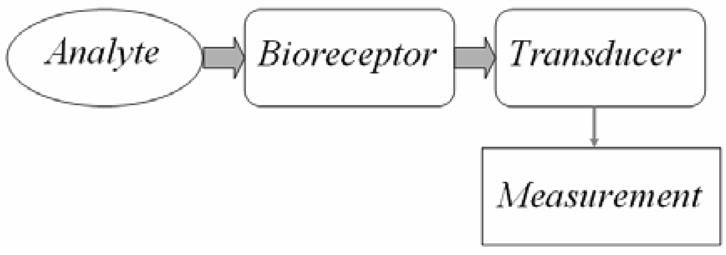
:1. Introduction
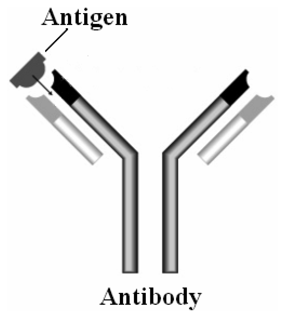
2. Bio receptors
3. Optical Transduction Mechanisms
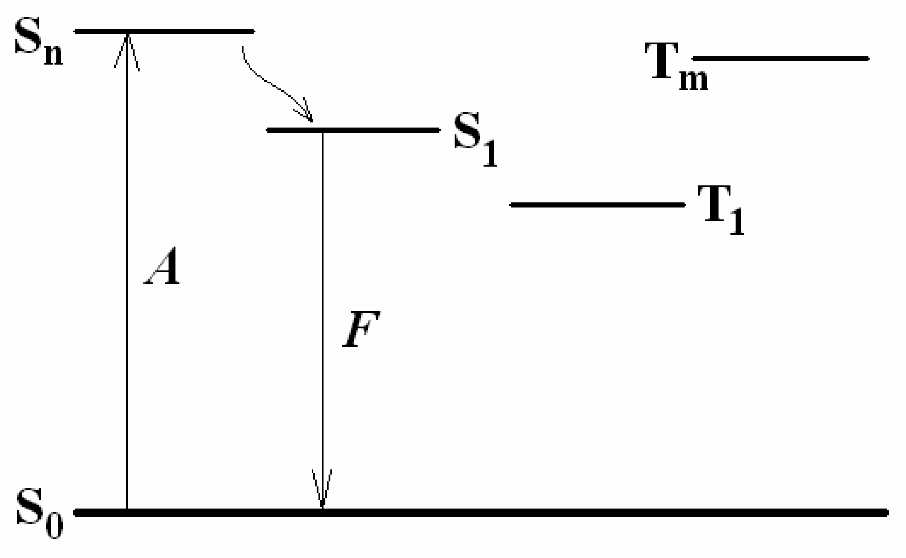
3.1 Fluorescence
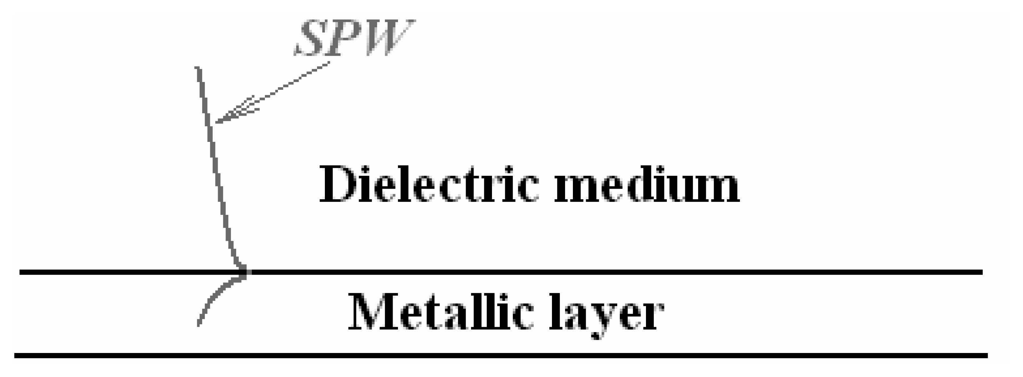
3.2 Surface Plasmon Resonance
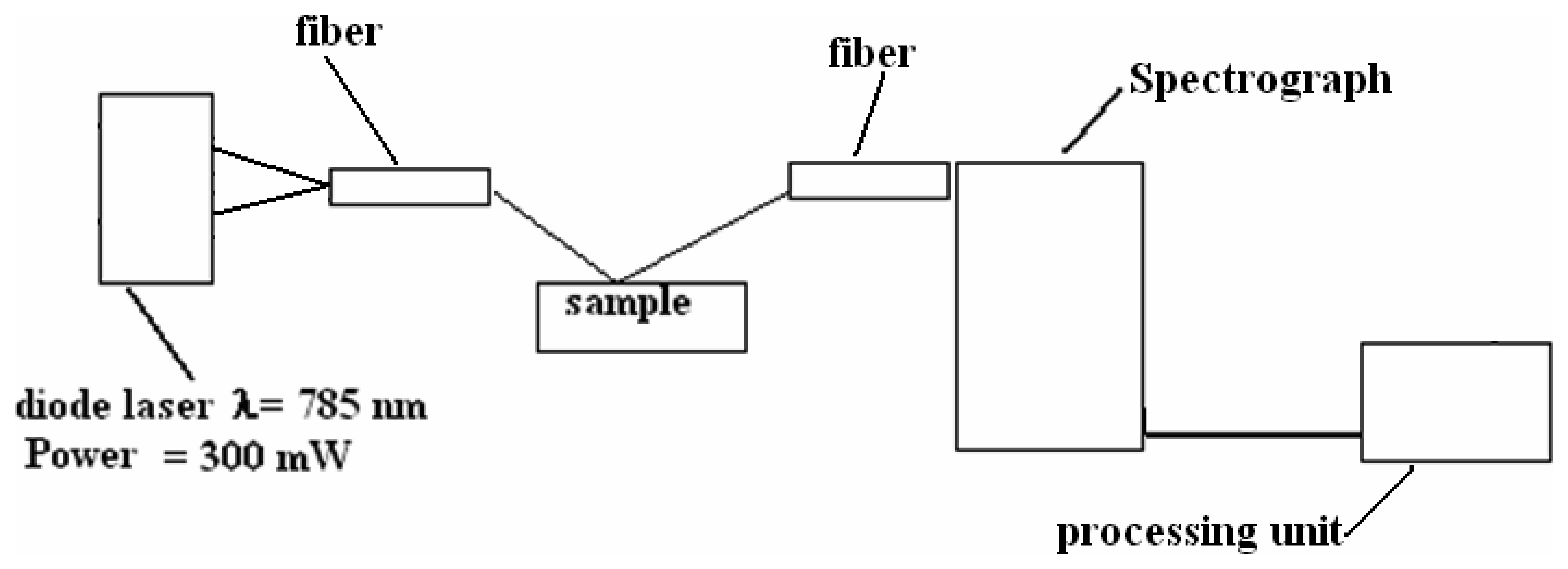
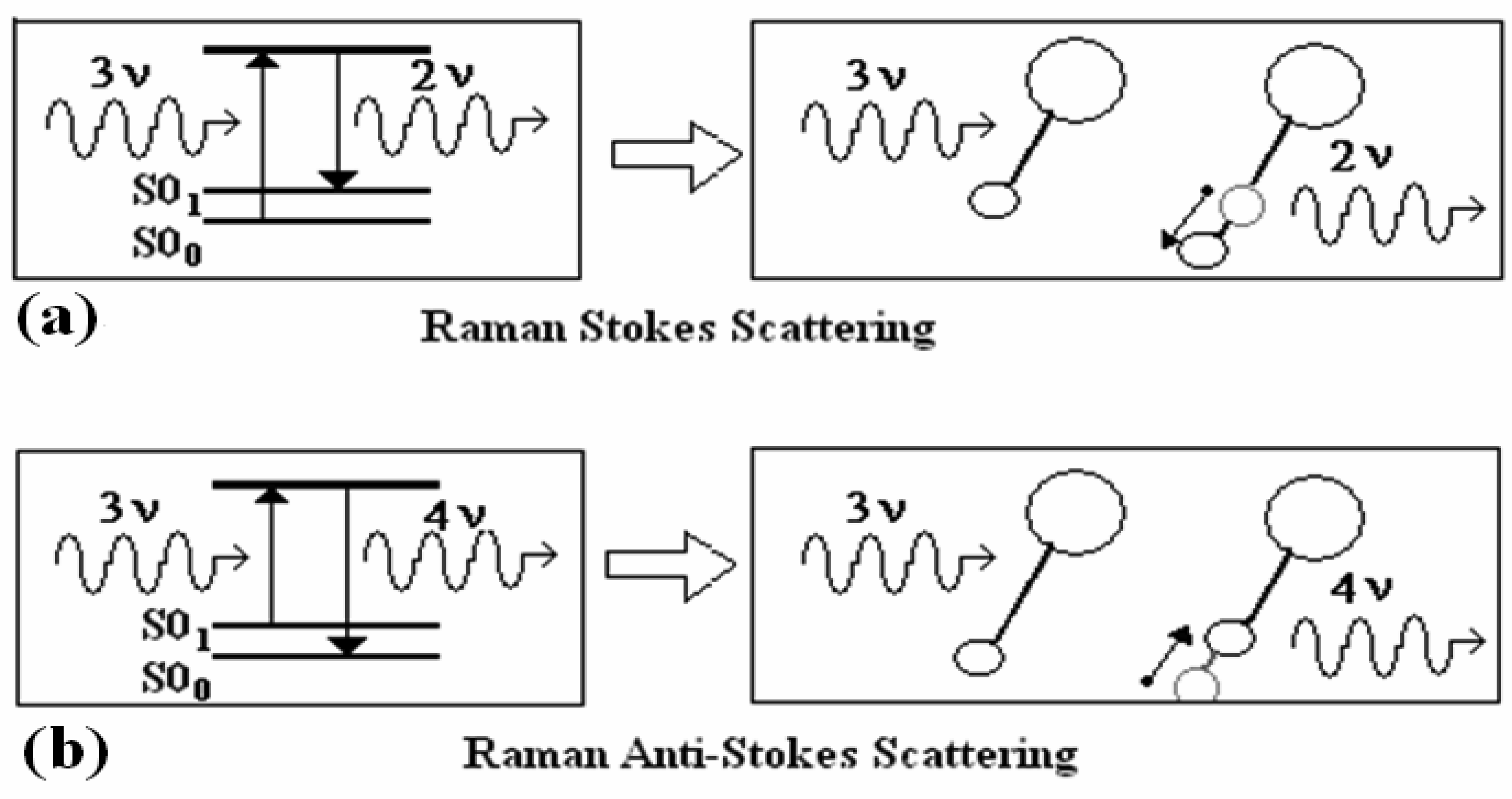
3.3 Raman Scattering
3.4 Absorption change
3.5 Photon migration spectroscopy
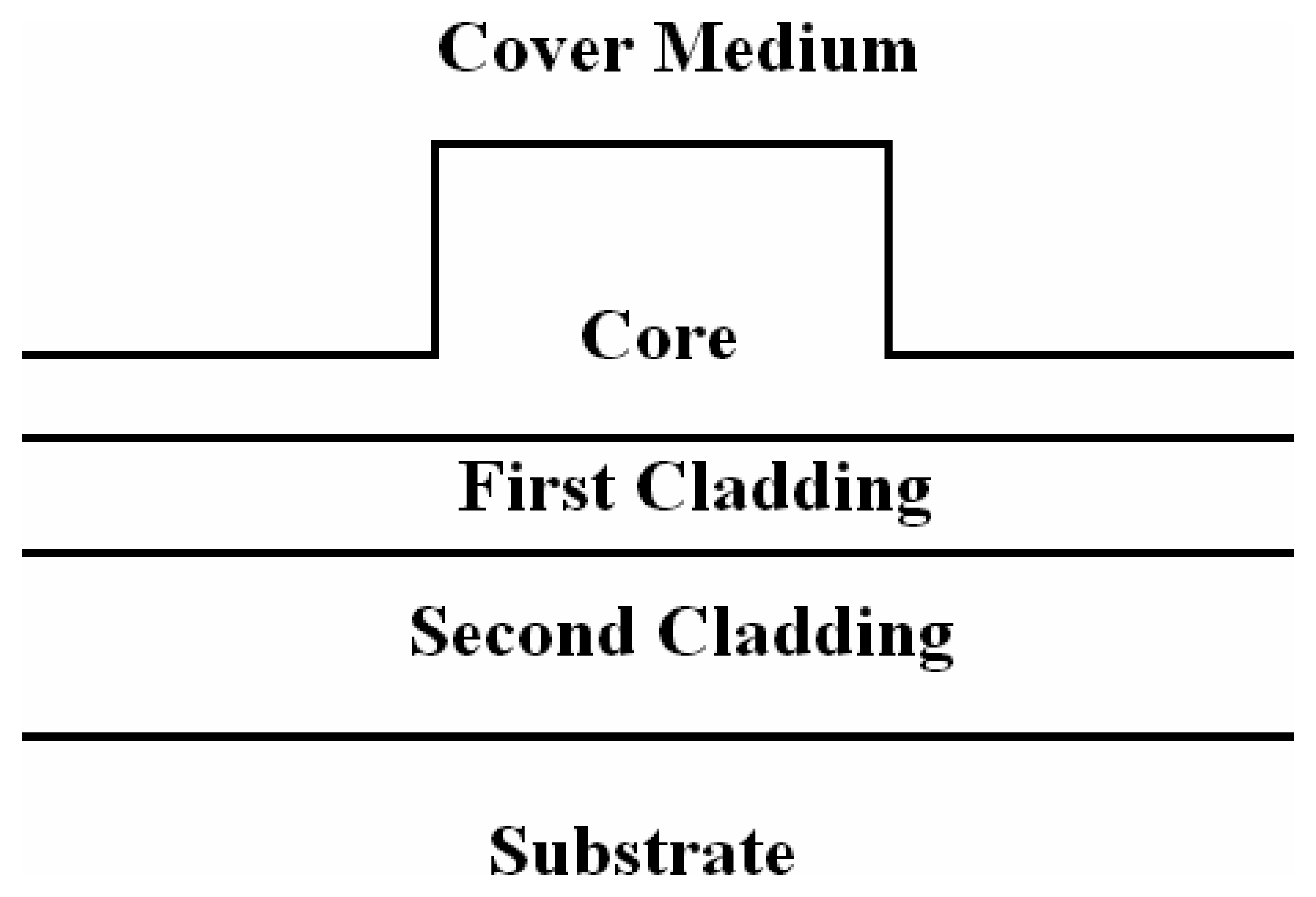
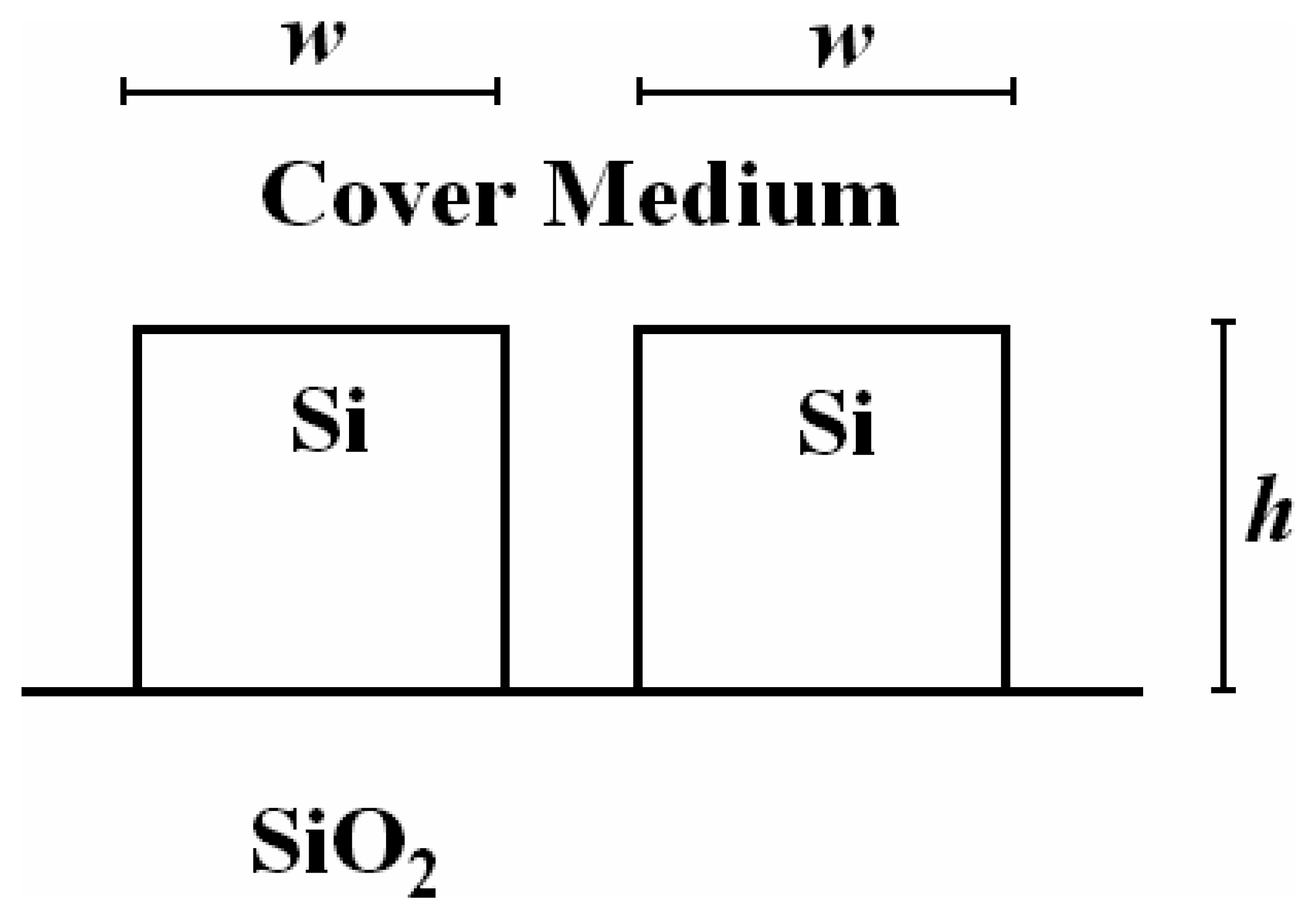
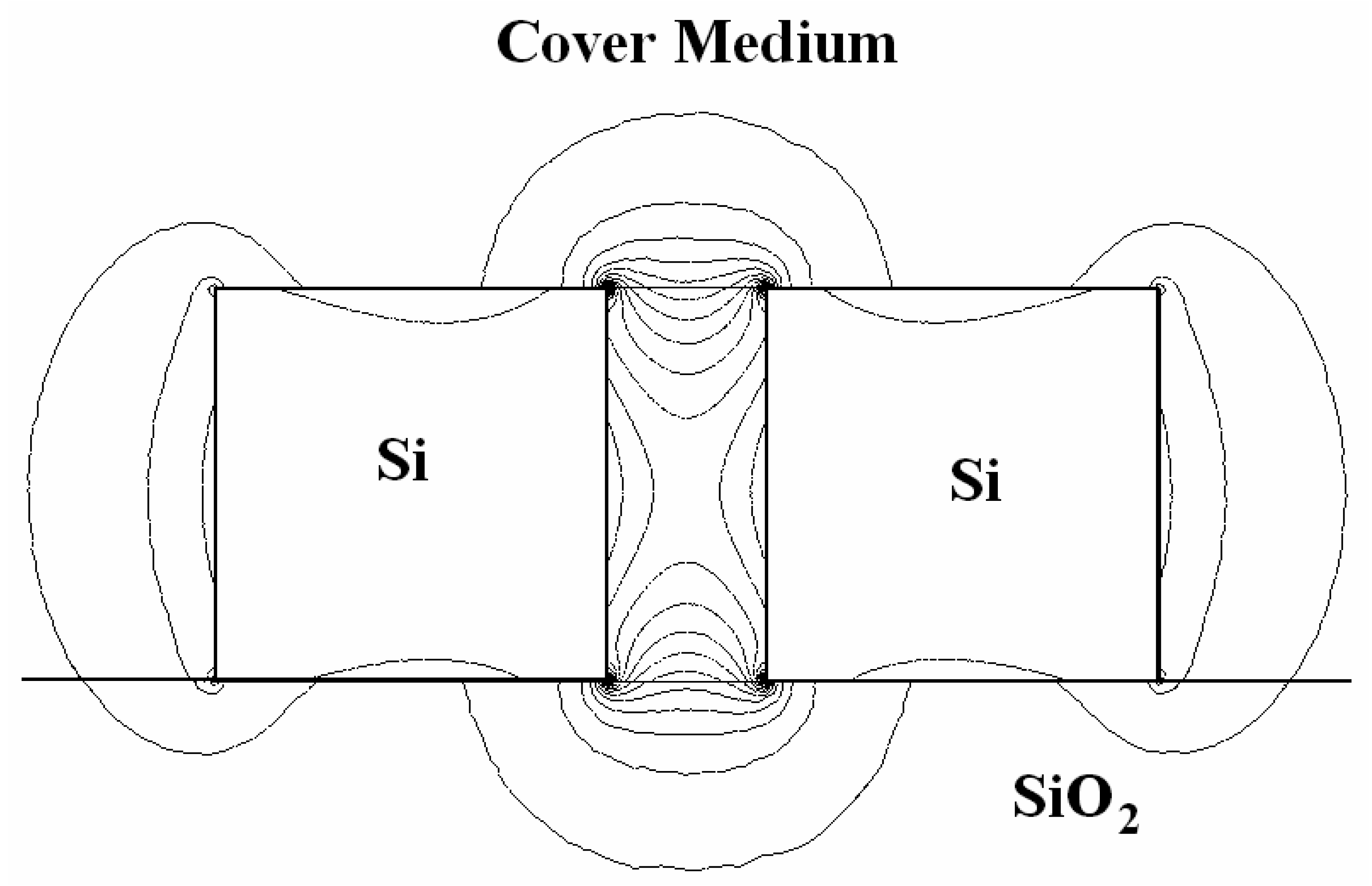
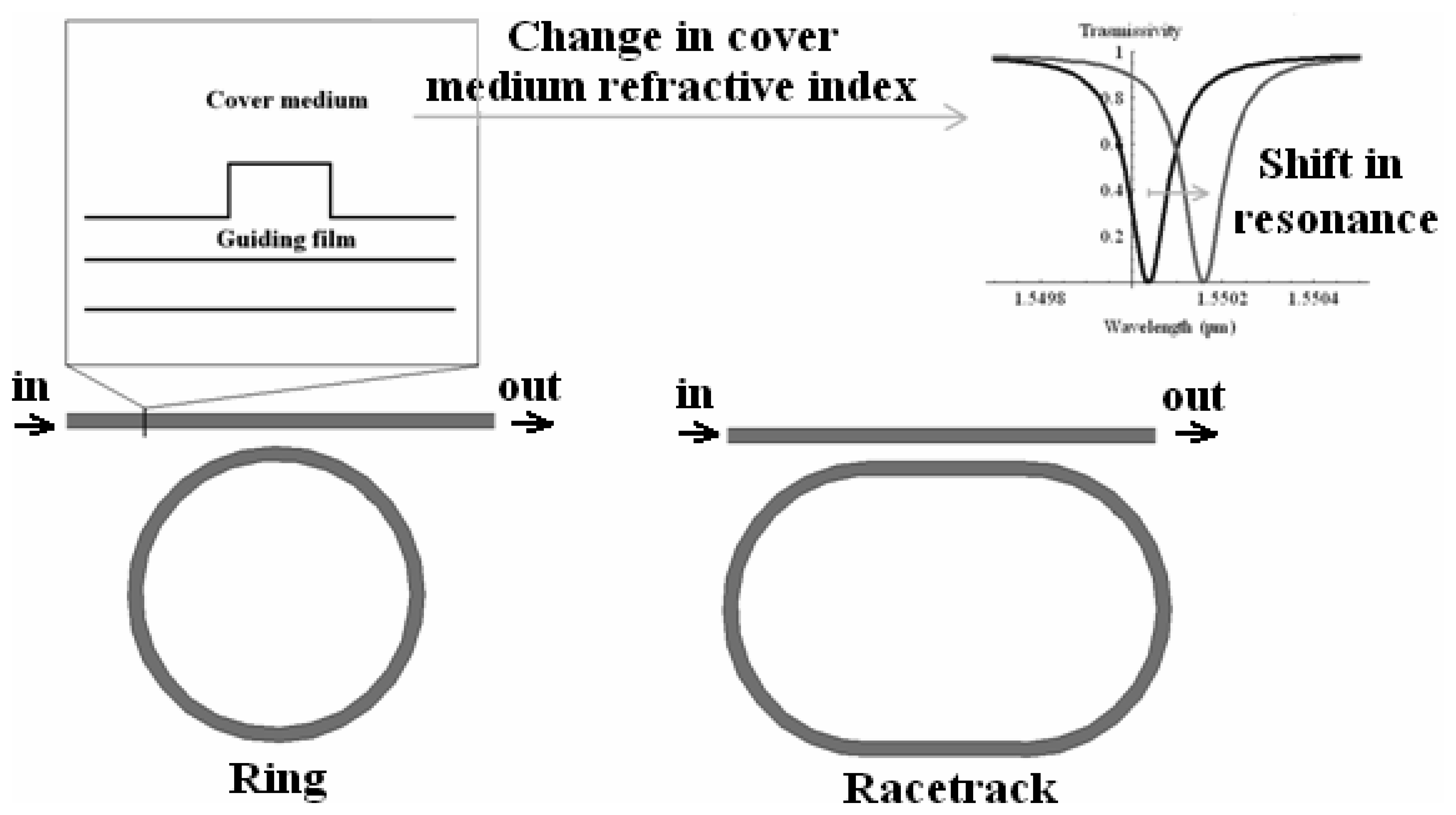
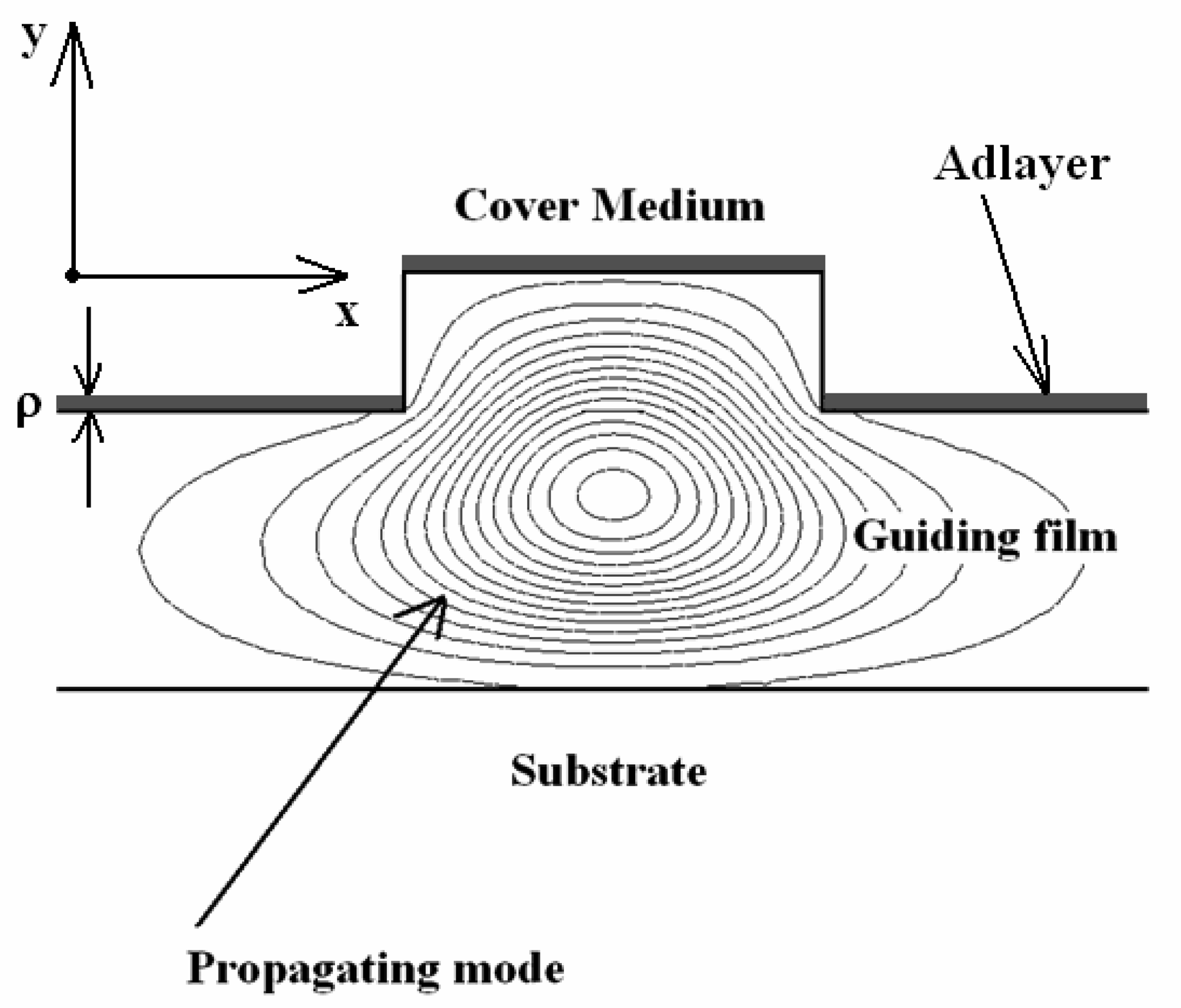
3.6 Effective index change in guiding structures
- i)
- the change of thickness (equal to ρ) of an adlayer constituted by adsorbed or bound molecules which are transported (by convection or diffusion) from the gaseous or liquid medium, that serves as waveguide cover medium, to cover medium/guiding film interface;
- ii)
- the change of refractive index nc of the homogeneous liquid that serves as waveguide cover medium.
4. Integrated optical biosensors
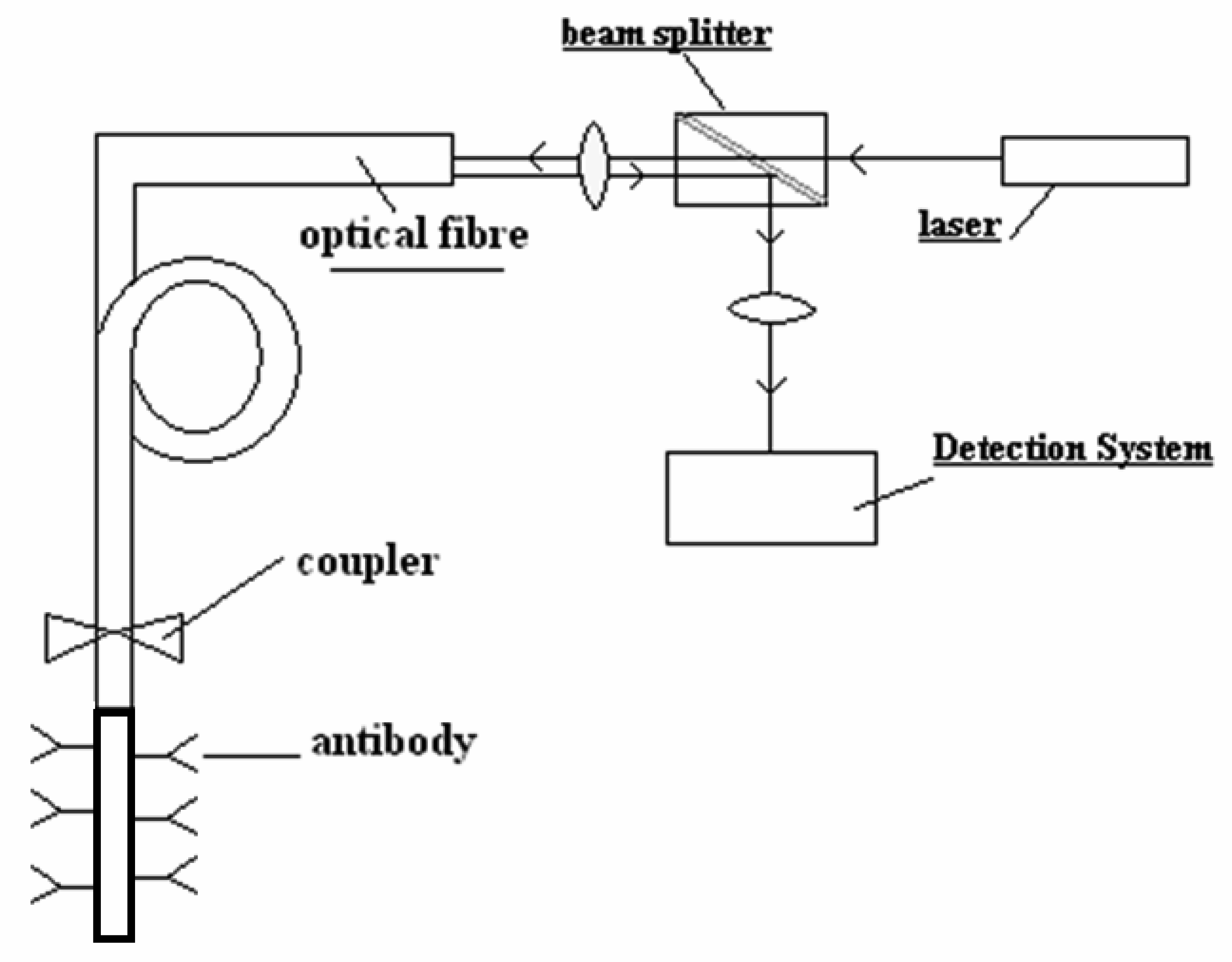
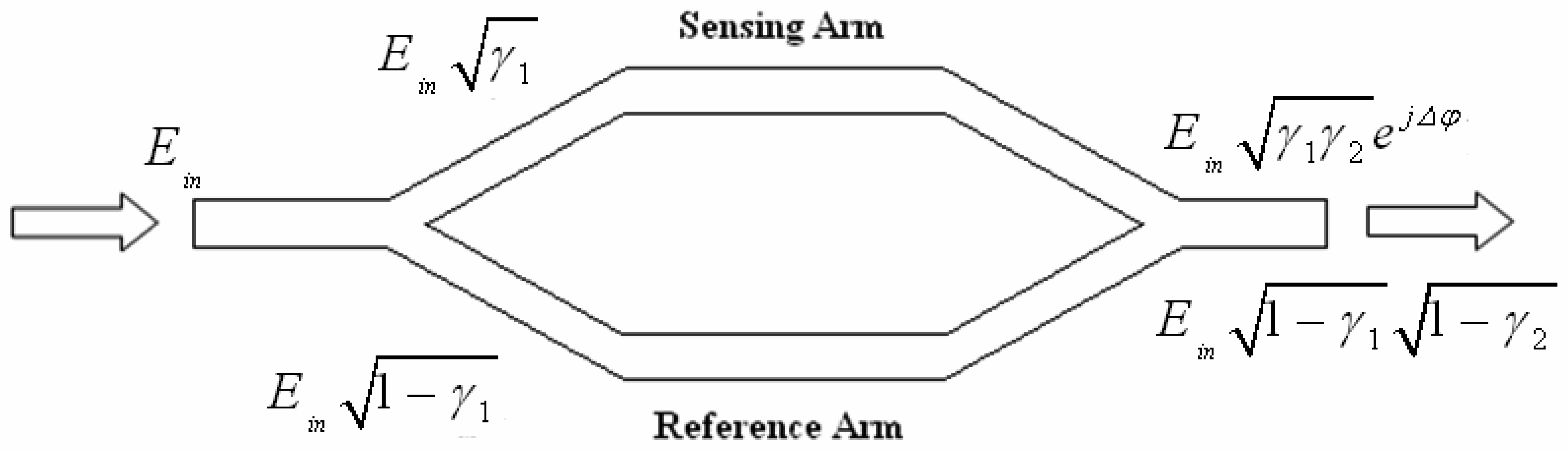
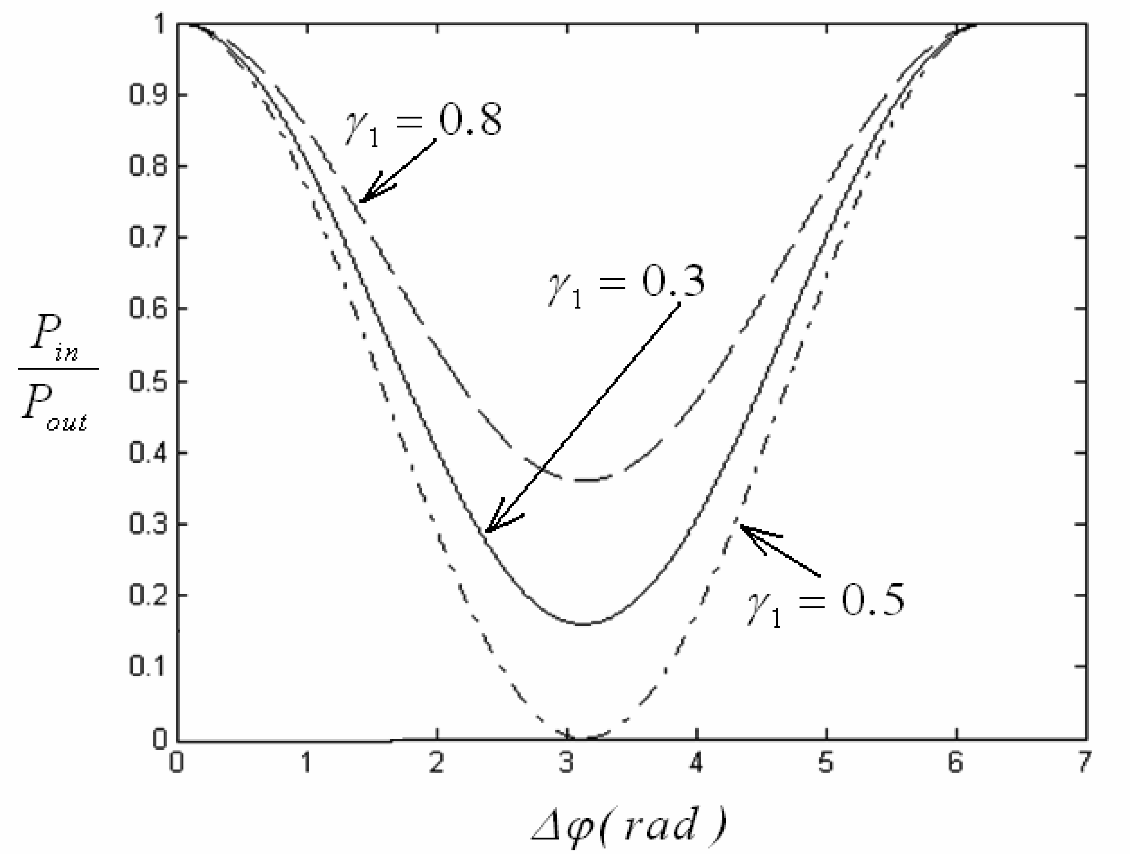
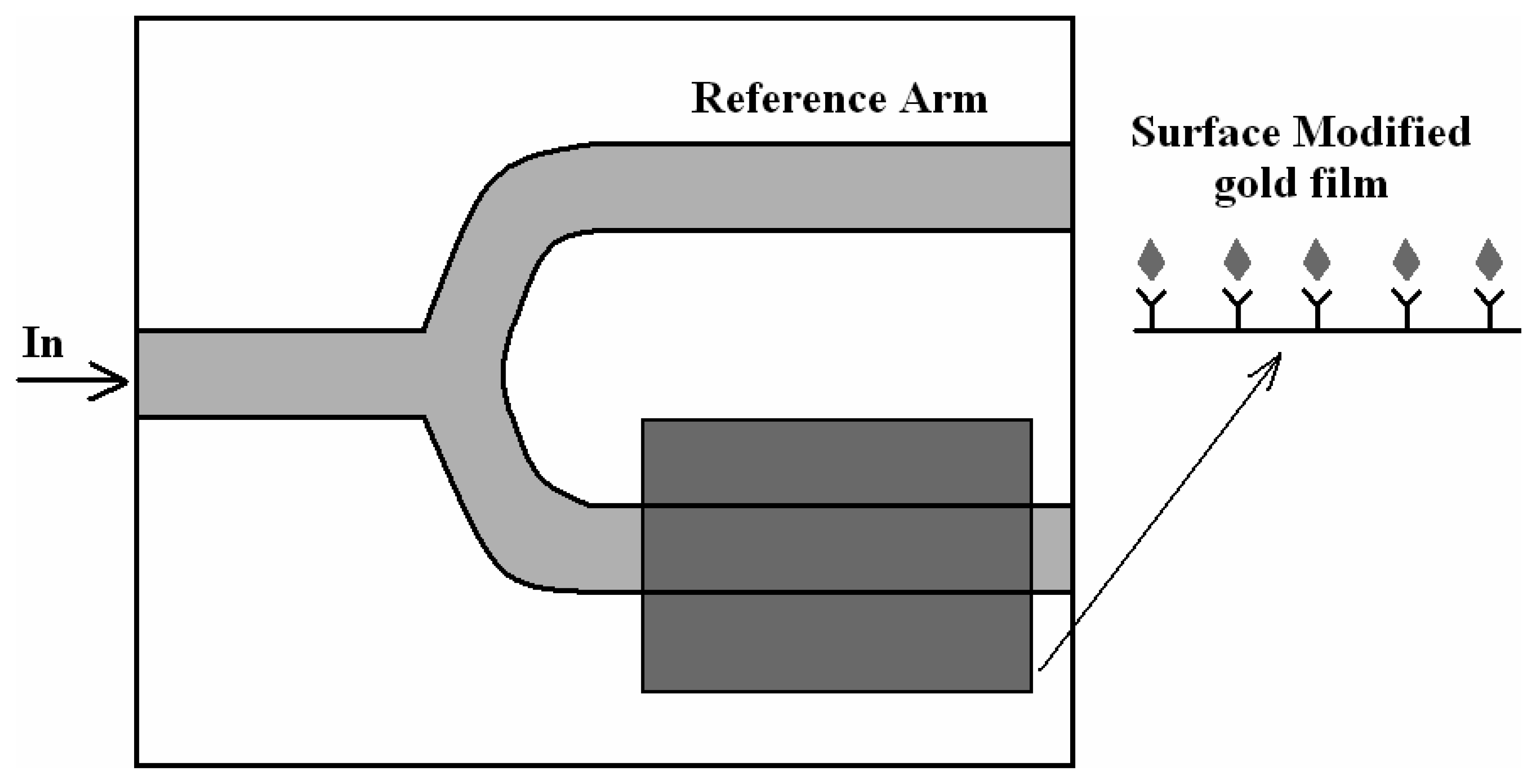
4.1 Interferometer architectures
4.2 Architectures based on anti-resonant reflecting optical waveguides
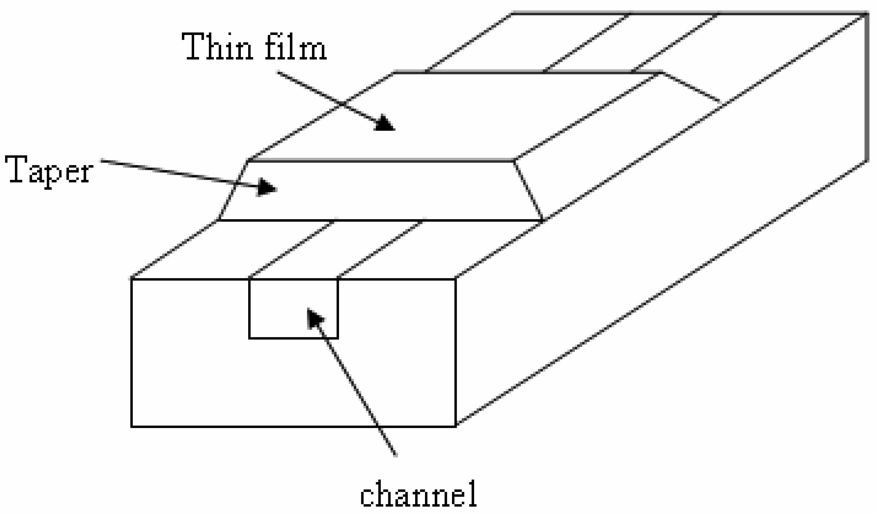
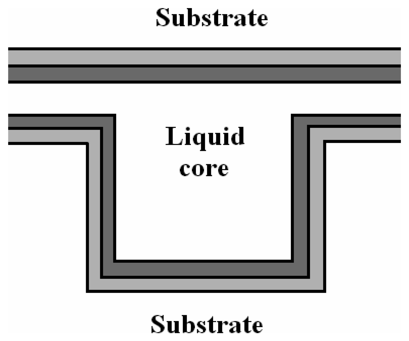
4.3 Architectures based on hollow waveguides
4.4 Architectures based on surface plasmon resonance
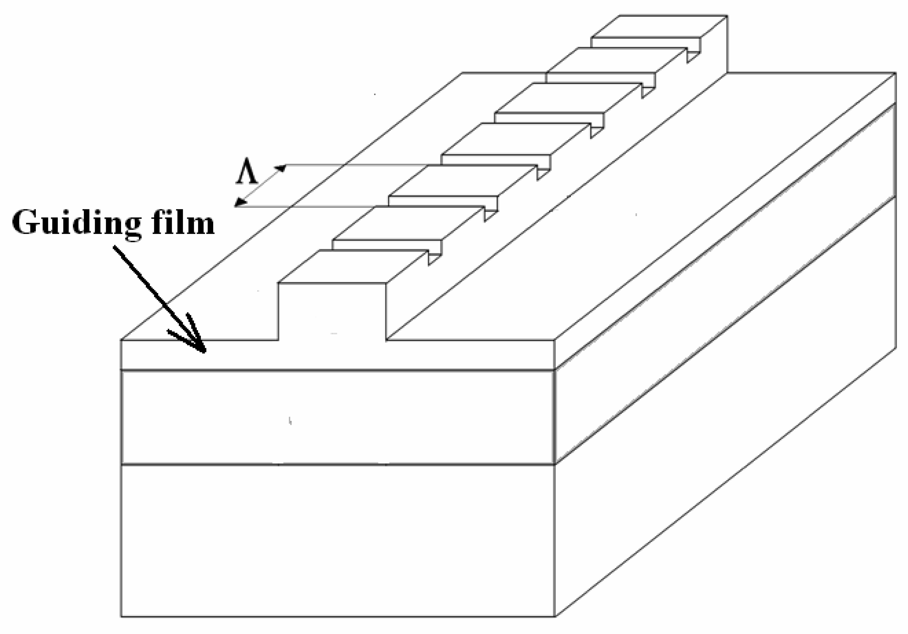
4.7 Architectures based on Bragg gratings
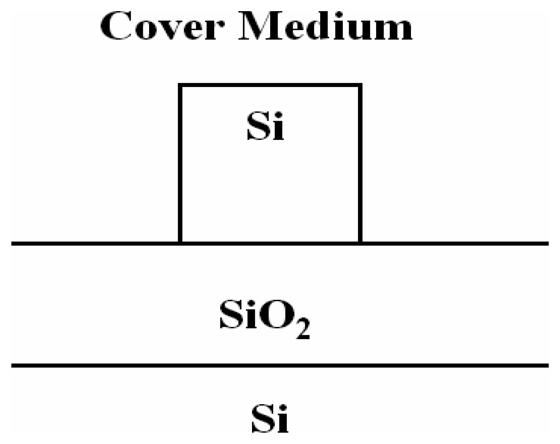
4.8 Architectures based on silicon slot waveguides
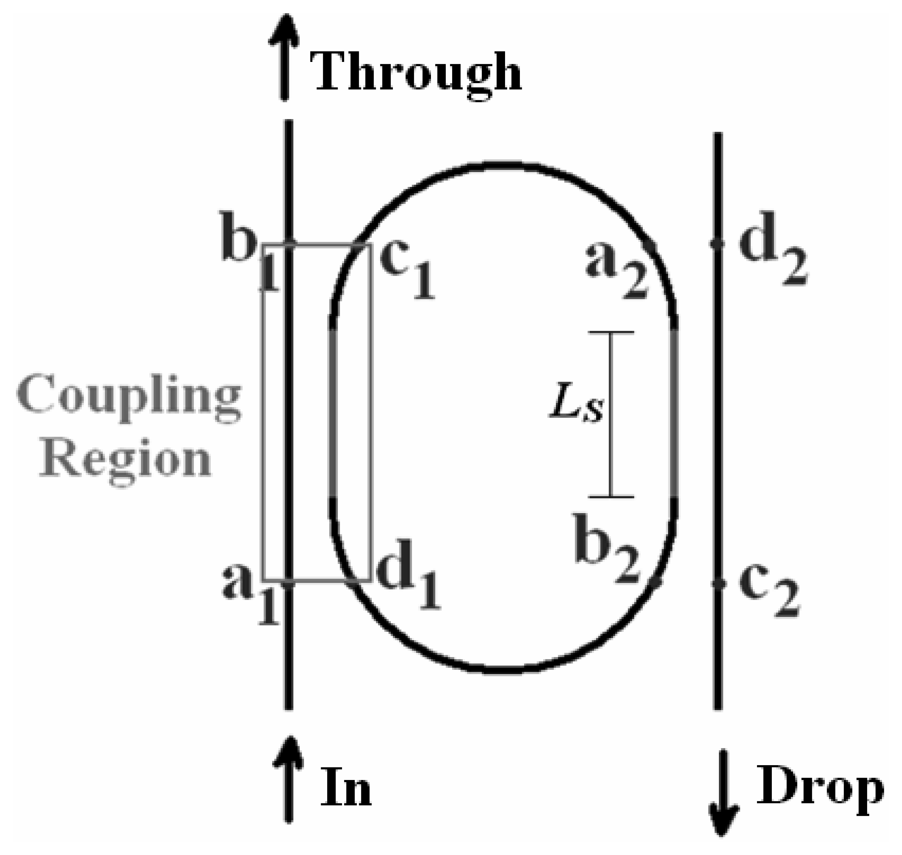
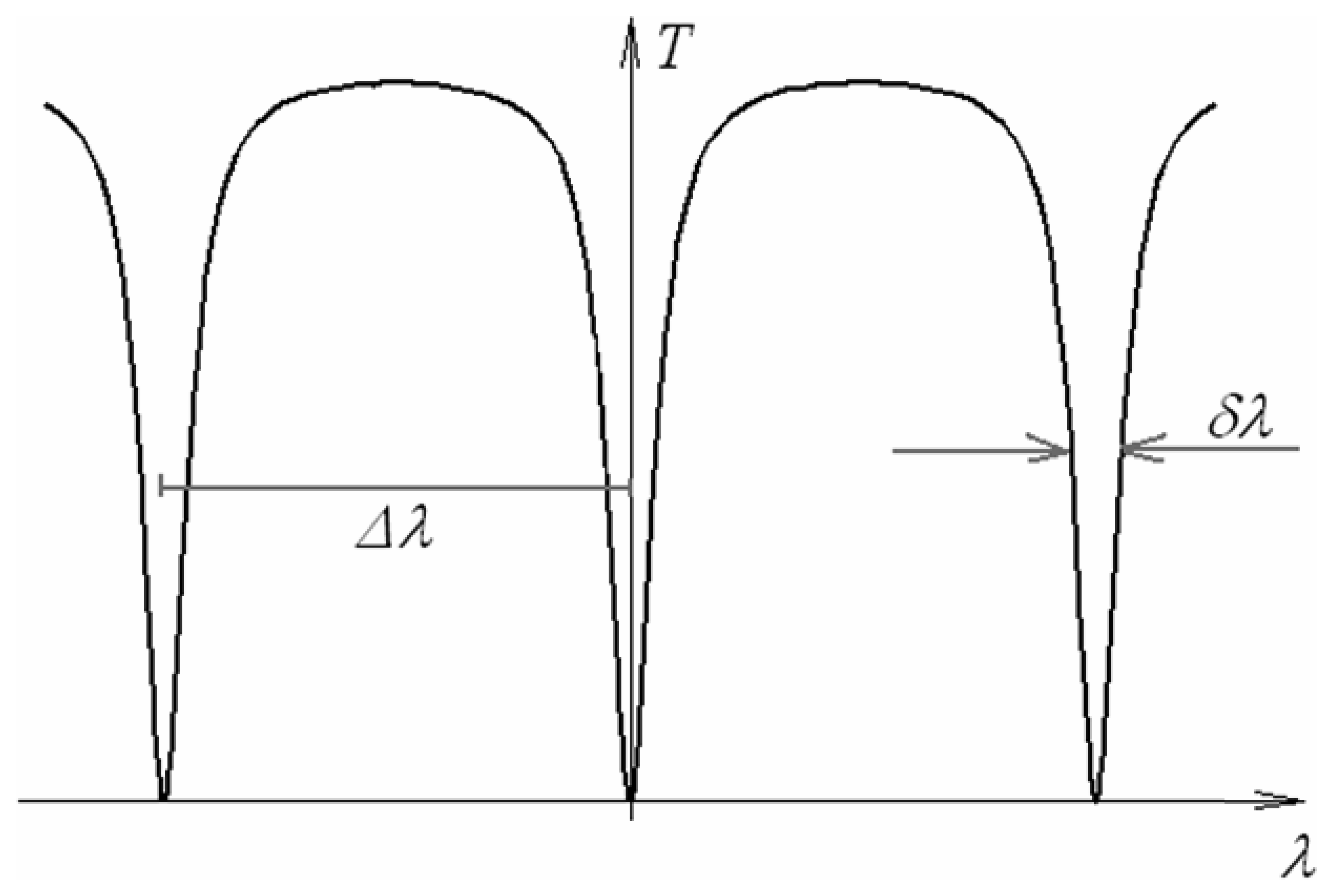
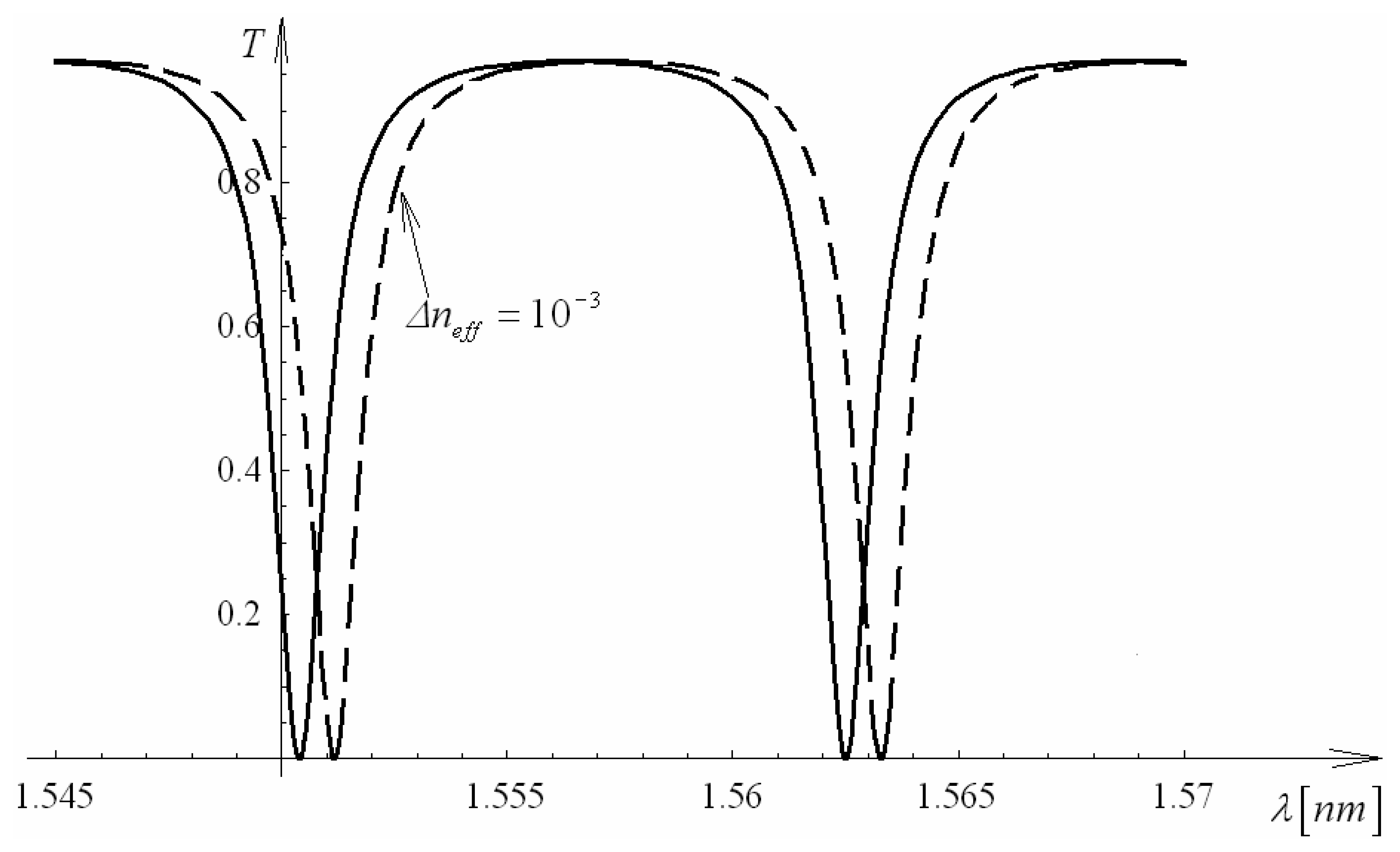
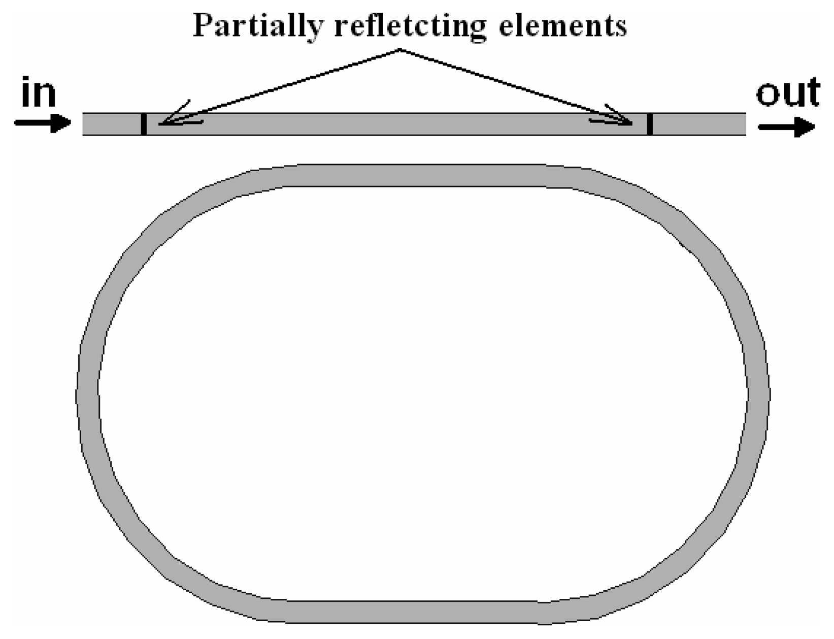
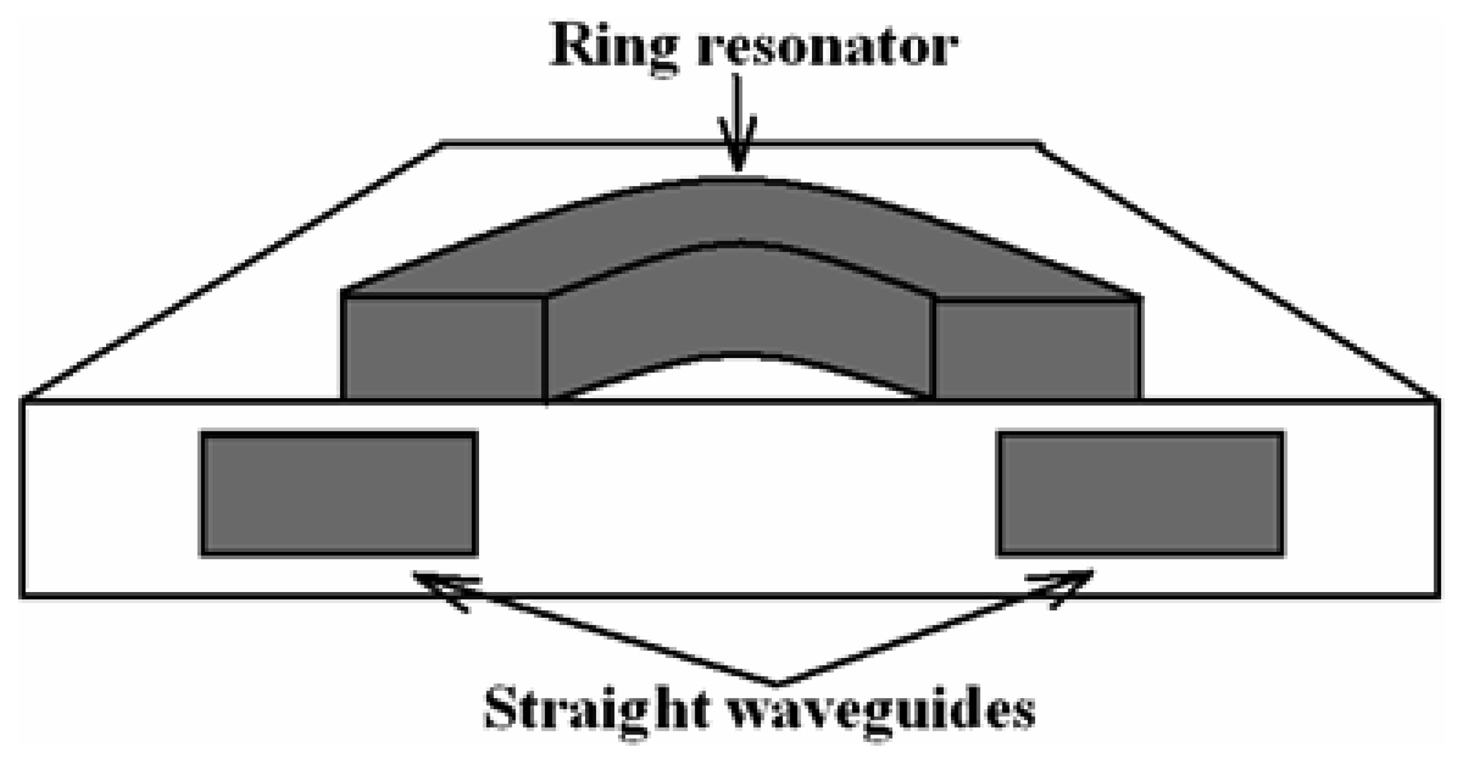
4.9 Architectures based on integrated optical micro cavities
5. Performance comparison
6. Conclusions
References
- Vo-Dinh, T.; Allain, L. Biosensors for Medical Applications. 2003; In Biomedical Photonics Handbook; Vo-Dinh, T., Ed.; Boca Raton; CRC Press. [Google Scholar]
- Vo-Dinh, T.; Cullum, B. M. Fluorescence Spectroscopy for Biomedical Diagnostics. 2003; In Biomedical Photonics Handbook; Vo-Dinh, T., Ed.; Boca Raton; CRC Press. [Google Scholar]
- Vo-Dinh, T.; Tromberg, B. J.; Griffin, G. D.; Ambrose, K. R.; Sepaniak, M. J.; Gardenhire, E. M. Antibody-based fiberoptics biosensor for the carcinogen benzo(a)pyrene. Appl. Spectrosc. 1987, 41, 735–738. [Google Scholar]
- Vo-Dinh, T.; Nolan, T.; Cheng, Y.E.; Sepaniak, M.J.; Alarie, J.P. Phase-resolved fiberoptics fluoroimmunosensor. Appl. Spectrosc. 1990, 44, 128–134. [Google Scholar]
- Smith, L. M.; Saunders, J. Z.; Kaiser, R. J.; Hughes, P.; Dodd, C. R.; Cornell, C. R.; Heiner, C.; Kent, S. B. H.; Hood, L. E. Fluorescence Detection in Automated DNA Sequence Analysis. Nature 1986, 321, 674–679. [Google Scholar]
- Homola, J.; Yee, S. S.; Gaugliz, G. Surface plasmon resonance sensors: review. Sens. Actuators B 1999, 54, 3–15. [Google Scholar]
- Flanagan, M. T.; Pantell, R.H. Surface plasmon resonance and immunosensors. Electron. Lett. 1984, 20, 968–970. [Google Scholar]
- Mahadevan-Jansen, A. Raman Spectroscopy: From Benchtop to Bedside. 2003; In Biomedical Photonics Handbook; Vo-Dinh, T., Ed.; Boca Raton; CRC Press. [Google Scholar]
- Isola, N. R.; Stokes, D. L.; Vo-Dinh, T. Surface enhanced Raman gene probe for HIV detection. Anal. Chem. 1998, 70, 1352–1356. [Google Scholar]
- Vo-Dinh, T.; Stokes, D. L.; Griffin, G. D.; Volkan, M.; Kim, U. J.; Simon, M. I. Surface-enhanced Raman scattering (SERS) method and instrumentation for genomics and biomedical analysis. J. Raman Spectrosc. 1999, 30, 785–793. [Google Scholar]
- Yotter, R. A.; Lee, L. A.; Wilson, D. M. Sensor technologies for monitoring metabolic activity in single cells – part II: nonoptical methods and applications. IEEE Sensors Journal 2004, 4, 395–411. [Google Scholar]
- Cerussi, A. E.; Tromberg, B. J. Photon Migration Spectroscopy Frequency-Domain Tecniques. 2003; In Biomedical Photonics Handbook; Vo-Dinh, T., Ed.; Boca Raton; CRC Press. [Google Scholar]
- Lillie, J. J.; Thomas, M. A.; Jokerst, N. M.; Ralph, S. E.; Dennis, K. A.; Handerson, C. L. Multimode interferometric sensors on silicon optimized for fully integrated complementary-metal-oxide-semiconductor chemical-biological sensor systems. J. Opt. Soc. Am. B 2006, 23, 642–651. [Google Scholar]
- Luo, D. H.; Levy, R. A.; Hor, Y. F.; Federici, J. F.; Pafchek, R. M. An integrated photonic sensor for in situ monitoring of hazardous organics. Sens. Actuators B 2003, 92, 121–126. [Google Scholar]
- Luff, B. J.; Wilkinson, J. S.; Piehler, J.; Hollenbach, U.; Ingenhoff, J.; Fabricius, N. Integrated optical Mach-Zehnder biosensor. J. Lightwave Technol. 1998, 16, 583–592. [Google Scholar]
- Brosinger, F.; Freimuth, H.; Lacher, M.; Ehrfeld, W.; Gedig, E.; Katerkanp, A.; Spener, F.; Cammann, K. A label-free affinity sensor with compensation of unspecific protein interaction by a highly sensitive integrated optical Mach-Zehnder interferometer on silicon. Sens. Actuators B 1997, 44, 350–355. [Google Scholar]
- Weisser, M.; Tovar, G.; Mittler-Neher, S.; Knoll, W.; Brosinger, F.; Freimuth, H.; Lacher, M.; Ehrfeld, W. Specific bio-recognition reactions observed with an integrated Mach–Zehnder interferometer. Biosensors & Bioelectronics 1999, 14, 405–411. [Google Scholar]
- Qui, Z.; Matsuda, N.; Itoh, K.; Murabayashi, M.; Lavers, C. R. A design for improving the sensitivity of a Mach-Zehnder interferometer to chemical and biological measurands. Sens. Actuators B: Chem. 2002, 81, 254–258. [Google Scholar]
- Kerrat, R.; Jaffrezic-Renault, N.; Greco, P.; Helmers, H.; Benech, P.; Rimet, R. Integrated optical enlarged-field interferometer used as a chemical sensor. Sens. Actuators B: Chem. 1996, 37, 7–11. [Google Scholar]
- Maisenholder, B.; Zappe, H. P.; Kunz, R. E.; Riel, P.; Moser, M.; Edlinger, J. A GaAs/AlGaAs-based refractometer platform for integrated optical sensing applications. Sens. Actuators B: Chem. 1997, 38, 324–329. [Google Scholar]
- Prieto, F.; Sepulveda, B.; Calle, A.; Llobera, A.; Dominguez, C.; Abad, A.; Montoya, A.; Lechuga, L. M. An integrated optical interferometric nanodevice based on silicon technology for biosensor applications. Nanotechnol. 2003, 14, 907–912. [Google Scholar]
- Drapp, B.; Piehler, J.; Brecht, A.; Gauglitz, G.; Luff, B. J.; Wilkinson, J. S.; Ingehoff, J. Integrated optical Mach-Zehnder interferometers as simazine immunoprobes. Sens. Actuators B 1997, 38, 277–282. [Google Scholar]
- Qi, Z.; Matsuda, N.; Itoh, K.; Murabayashi, M.; Lavers, C. R. A design for improving the sensitivity of a Mach-Zehnder interferometer to chemical and biological measurands. Sens. Actuators B 2002, 81, 254–258. [Google Scholar]
- Ymeti, A.; Kanger, J. S.; Greve, J.; Lambeck, P. V.; Wijn, R.; Heideman, R. G. Realization of a multichannel integrated Young interferometer chemical sensor. Appl. Opt. 42. [Google Scholar]
- Prieto, F.; Llobera, A.; Jiménez, D.; Doménguez, C.; Calle, A.; Lechuga, L. M. Design and Analysis of Silicon Antiresonant Reflecting Optical Waveguides for Evanescent Field Sensor. J. Lightwave Technol. 2000, 18, 966–972. [Google Scholar]
- Prieto, F.; Lechuga, L.M.; Calle, A.; Llobera, A.; Domínguez, C. Optimized Silicon Antiresonant Reflecting Optical Waveguides for Sensing Applications. J. Lightwave Technol. 2001, 19, 75–83. [Google Scholar]
- Benaissa, K.; Nathan, A. Silicon anti-resonant reflecting optical waveguides for sensor applications. Sens. Actuators B 1998, 65, 33–44. [Google Scholar]
- Prieto, F.; Sepulveda, B.; Calle, A.; Llobera, A.; Dominguez, C.; Lechuga, L. M. Integrated Mach-Zehnder interferometer based on ARROW structures for biosensor applications. Sens. Actuators B 2003, 92, 151–158. [Google Scholar]
- Campopiano, S.; Bernini, R.; Zeni, L.; Sarro, P. M. Microfluidic sensor based on integrated optical hollow waveguides. Opt. Lett. 2004, 29, 1894–1896. [Google Scholar]
- Harris, R. D.; Luff, B. J.; Wilkinson, J. S.; Piehler, J.; Brecht, A.; Gauglitz, G.; Abuknesha, R. A. Integrated optical surface plasmon resonance immunoprobe for simazine detection. Biosensors & Bioelectron. 1999, 14, 377–386. [Google Scholar]
- Dostalek, J.; Ctyroky, J.; Homola, J.; Brynda, E.; Skalsky, M.; Nekvindova, P.; Spirkova, J.; Skvor, J.; Schrofel, J. Surface plasmon resonance biosensor based on integrated optical waveguide. Sens. Actuators B 2001, 76, 8–12. [Google Scholar]
- Homola, J.; Koudela, I.; Yee, S. S. Surface plasmon resonance sensors based on diffraction gratings and prism couplers: sensitivity comparison. Sens. Actuators B 1999, 54, 16–24. [Google Scholar]
- Veldhuis, G.J.; Berends, J.H.; Heideman, R.G.; Lambeck, P.V. An integrated optical Bragg reflector used as a chemo-optical sensor. Pure Appl. Opt. 1998, 7, L23–L26. [Google Scholar]
- Hopman, W. C. L.; Pottier, P.; Yudistira, D.; van Lith, J.; Lambeck, P. V.; De La Rue, R. M.; Driessen, A.; Hoekstra, H. J. W. M.; de Ridder, R. M. Quasi one-dimensional photonic crystal as a compact building-block for refractometric optical sensors. IEEE J. Sel. Top. in Quantum Electron. 2005, 11, 11–16. [Google Scholar]
- Densmore, A.; Xu, D.-X.; Waldron, P.; Janz, S.; Cheben, P.; Lapointe, J.; Delâge, A.; Lamontagne, B.; Schmid, J. H.; Post, E. A Silicon-on-Insulator Photonic Wire Based Evanescent Field Sensor. IEEE Photon. Tech. Lett. 2006, 18, 2520–2522. [Google Scholar]
- Xu, Q.; Almeida, V. R.; Panepucci, R. R.; Lipson, M. Experimental demonstration of guiding and confining light in nanometer-size low-refractive-index material. Opt. Lett. 2004, 29, 1626–1628. [Google Scholar]
- Dell'Olio, F.; Passaro, V. M. N. Optical sensing by optimized silicon slot waveguides. Optics Express 2007, 15, 4977–4993. [Google Scholar]
- Xia, F.; Sekaric, L.; Vlasov, Y. A. Mode conversion losses in silicon-on-insulator photonic wire based racetrack resonators. Optics Express 2006, 14, 3872–3886. [Google Scholar]
- De Vos, K.; Bertolozzi, I.; Bienstman, P.; Baets, R.; Schacht, E. Optical Biosensor based on Silicon-on-Insulator Microring Resonators for Specific Protein Binding Detection. Proc. of Symposium IEEE/LEOS Benelux Chapter; 2006; pp. 213–216. [Google Scholar]
- Dell'Olio, F.; Passaro, V. M. N. Ammonia optical sensor based on microring resonator. Proc. of 11th International Meeting on Chemical Sensors; 2006; p. 27. [Google Scholar]
- Dell'Olio, F.; Passaro, V. M. N.; De Leonardis, F. Surface Sensitivity Optimization of a Microring Resonator for Biochemical Sensing. Int. Conf. on Tran. Opt. Net. (ICTON) Proc., Nottingham, 18-22 June, 2006; 4, pp. 128–131.
- Chao, C.-Y.; Guo, L. J. Biochemical sensors based on polymer microrings with sharp asymmetrical resonance. Appl. Phys. Lett. 2003, 83, 1527–1529. [Google Scholar]
- Chao, C.-Y.; Fung, W.; Guo, L. J. Polymer microring resonators for Biochemical Sensing Applications. IEEE J. Sel. Top. in Quantum Electron. 2006, 12, 134–142. [Google Scholar]
- Yalçin, A.; Popat, K. C.; Aldridge, J. C.; Desai, T. A.; Hryniewicz, J.; Chbouki, N.; Little, B. E.; King, O.; Van, V.; Chu, S.; Gill, D.; Anthes-Washburn, M.; Selim Unlu, M.; Goldberg, B. B. Optical sensing of biomelecules using microring resonators. IEEE J. Sel. Top. in Quantum Electron. 2006, 12, 148–155. [Google Scholar]
- Ksendzov, A.; Lin, Y. Integrated optics ring-resonator sensors for protein detection. Opt. Lett. 2005, 30, 3344–3346. [Google Scholar]
- Krioukov, E.; Klunder, D. J. W.; Driessen, A.; Greve, J.; Otto, C. Sensor based on an integrated optical cavity. Opt. Lett. 2002, 27, 512–514. [Google Scholar]


| Year | Author | Architecture | Technology | Detection limit | Total length [μm] |
|---|---|---|---|---|---|
| 1997 | B. Drapp et al. [22] | MZI | Glass | 1.5×10⁻⁶ | 15,000 |
| 1999 | R.D. Harris et al. [30] | SPR | Glass | 1×10⁻⁴ | 2,000 |
| 2002 | E. Krioukov et al. [46] | Disk resonator | CMOS-compatible | 1×10⁻⁴ | 30 |
| 2003 | F. Prieto et al. [21] | MZI | CMOS-compatible | 7×10⁻⁶ | 30,000 |
| 2003 | A. Ymeti et al. [24] | Young | CMOS-compatible | 8.5×10⁻⁸ | ≈ 50,000 |
| 2003 | F. Prieto et al. [28] | MZI (ARROW) | CMOS-compatible | 2×10⁻⁵ | 15,000 |
| 2004 | S. Campopiano et al. [29] | Hollow | CMOS-compatible | 9×10⁻⁴ | 200,000 |
| 2005 | W. Hopman et al. [34] | Bragg grating | CMOS-compatible | 4×10⁻⁵ | 76 |
| 2006 | F. Dell'Olio et al. [40] | Ring resonator | SOI | 1×10⁻⁴ | 6 |
| 2006 | A. Yalçin et al. [44] | Ring resonator | Glass | 1.8×10⁻⁵ | 120 |
© 2007 by MDPI ( http://www.mdpi.org). Reproduction is permitted for noncommercial purposes.
Share and Cite
Passaro, V.M.N.; Dell’Olio, F.; Casamassima, B.; De Leonardis, F. Guided-Wave Optical Biosensors. Sensors 2007, 7, 508-536. https://doi.org/10.3390/s7040508
Passaro VMN, Dell’Olio F, Casamassima B, De Leonardis F. Guided-Wave Optical Biosensors. Sensors. 2007; 7(4):508-536. https://doi.org/10.3390/s7040508
Chicago/Turabian StylePassaro, Vittorio M. N., Francesco Dell’Olio, Biagio Casamassima, and Francesco De Leonardis. 2007. "Guided-Wave Optical Biosensors" Sensors 7, no. 4: 508-536. https://doi.org/10.3390/s7040508
APA StylePassaro, V. M. N., Dell’Olio, F., Casamassima, B., & De Leonardis, F. (2007). Guided-Wave Optical Biosensors. Sensors, 7(4), 508-536. https://doi.org/10.3390/s7040508