Miniaturized, Planar Ion-selective Electrodes Fabricated by Means of Thick-film Technology

Koncki
*
Author to whom correspondence should be addressed.
Sensors 2006, 6(4), 390-396; https://doi.org/10.3390/s6040390
Submission received: 2 November 2005
/
Accepted: 26 January 2006
/
Published: 7 April 2006
Abstract
:Various planar technologies are employed for developing solid-state sensors having low cost, small size and high reproducibility; thin- and thick-film technologies are most suitable for such productions. Screen-printing is especially suitable due to its simplicity, low-cost, high reproducibility and efficiency in large-scale production. This technology enables the deposition of a thick layer and allows precise pattern control. Moreover, this is a highly economic technology, saving large amounts of the used inks. In the course of repetitions of the film-deposition procedure there is no waste of material due to additivity of this thick-film technology. Finally, the thick films can be easily and quickly deposited on inexpensive substrates. In this contribution, thick-film ion-selective electrodes based on ionophores as well as crystalline ion-selective materials dedicated for potentiometric measurements are demonstrated. Analytical parameters of these sensors are comparable with those reported for conventional potentiometric electrodes. All mentioned thick-film strip electrodes have been totally fabricated in only one, fully automated thick-film technology, without any additional manual, chemical or electrochemical steps. In all cases simple, inexpensive, commercially available materials, i.e. flexible, plastic substrates and easily cured polymer-based pastes were used.
Introduction
Potentiometry is an attractive tool for many practical applications as it allows the determination of a wide spectrum of ions and because it applies a portable and inexpensive equipment. This analytical technique is especially useful for various medical and environmental tests carried at remote sites (‘in field’ measurements). Low-cost and small-size disposable electrode systems are desirable for these applications. Miniaturization and large-scale production are current trends in sensor development. Thick-film technology is especially suitable due to its simplicity, low-cost, high reproducibility and efficiency in large-scale production.
Screen-printing technology (as shown in Fig. 1) is especially recommended as simple and fast method for a large-scale production of strip amperometric electrodes [1-4]. The thick-film technology is rather rarely applied for the fabrication of potentiometric devices. In this contribution, thick-film ion-selective electrodes based on ionophores as well as crystalline ion-selective materials dedicated for potentiometric measurements are demonstrated.
Thick-film technology
Screen-printing is a well known technique for making patterns on various substrates (i.e., paper, plastic, wood, glass, ceramics, etc.). The main idea of this technology is very simple. This technique consists of two processes: preparation of a stencil and printing. The stencil must be created in the negative form of the requested pattern. Then, the stencil is put on the substrate and covered with a paint. That forms the image one has to create (Fig. 1). The possibility of using a few stencils and many different paints or pastes can lead to achieve more complex patterns. With this technique, the use of almost every paste, which can be deposited on almost every substrate, is possible.
Thick-film electrodes
The fabrication of the sensors by screen-printing technique is possible, because each chemical sensor, consisting of transducer, sensitive membrane and housing can be imagined as a system of layers (Fig. 2). In such a planar potentiometric electrode one layer can work as an electric contact of the electrode. The sensitive membrane can be the next layer, and finally, the insulating layer that represents (together with the substrate) an equivalent of a conventional electrode body.
Thick-film ion-selective electrodes
Using materials that after the screen-printing process will have the predicted physical and chemical properties allows the fabrication of planar electrochemical sensors. Potentiometric sensors can be fabricated in three steps: (A) printing of the paste that will form an electric contact of the sensor after curing, (B) printing of the paste that will be a sensitive element of the fabricated sensor, (C) printing of the paste that will be an insulating layer - analogue of conventional electrode body. The patterns used in this work are shown in Figure 3. The final product and the connector for such sensors are shown in Figure 4.
Ion-selective electrodes for the detection of potassium and ammonium ions had membranes made of conventional insulating paste, doped with ionophores (valinomycin and nonactin, respectively) and plasticizers (bis-(2-ethylhexyl) sebacate - DOS) commonly used for the fabrication of electrodes for these ions [5]. Membranes of solid-state electrodes for copper (II) and silver ions were made of graphite paste, doped with metal sulphide: Cu2S [6,7] and Ag2S [8], respectively. Analytical parameters of these sensors are comparable with those reported for conventional potentiometric electrodes. Typical responses and corresponding calibration graphs of the developed planar ion-selective electrodes are shown in Figure 5.
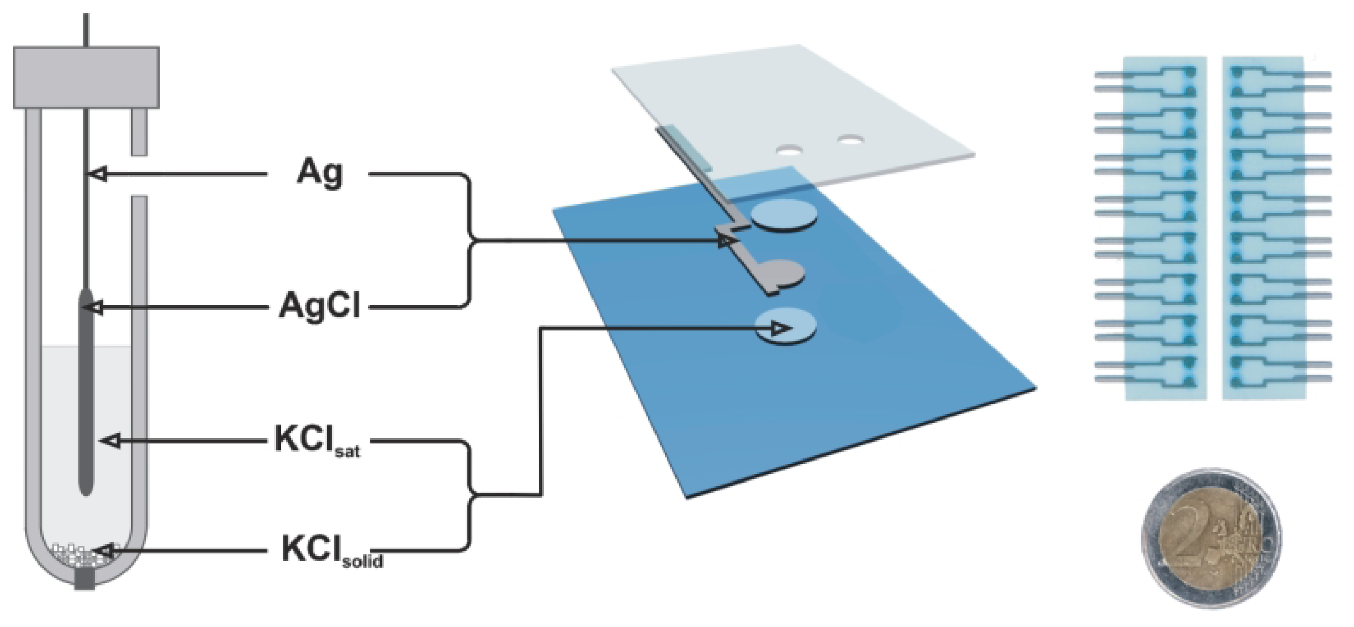
The reference electrode is the indispensable part of the complete electrochemical cell for potentiometric measurements. Such electrodes can be also obtained in planar format using thick-film technology [9]. The printing sequence of such a electrode was as follows: (A) protective paste doped with KCl, (B) Ag/AgCl paste, (C) protective paste doped with KCl, (D) non-modified protective paste. As previously, the electrodes were printed onto a flexible polyester foil. Scheme and design of these fully screen-printed reference electrodes are shown in Figure 6. These planar miniaturized electrodes could be used together with the thick-film sensors for obtaining various potentiometric cells [9].
Conclusions
Screen-printing technology can be useful for economic mass production of electrodes for potentiometric measurements. Analogues of solid-state electrodes as well as liquid ion-selective electrodes can be fabricated in this technology. It is also possible to fabricate an all-screen-printed reference electrode. The presented application of screen-printing technology is promising for the production of integrated potentiometric systems. Such integrated devices (complete electrochemical microcells) could be used as disposable devices as well as detectors in more advanced systems, i.e. FIA (flow-injection analysis).
References
- Galan-Vidal, C.A.; Munoz, J.; Dominguez, C.; Alegret, S. Chemical sensors, biosensors and thick-film technology. Trends in Analytical Chemistry 1995, 14, 225. [Google Scholar]
- Hart, J.P.; Wring, S.A. Recent developments in the design and application of screen-printed electrochemical sensors for biomedical, environmental and industrial analyses. Trends in Analytical Chemistry 1997, 16, 89. [Google Scholar]
- Honeychurch, K.C.; Hart, J.P. Screen-printed electrochemical sensors for monitoring metal pollutants. Trends in Analytical Chemistry 2003, 22, 456. [Google Scholar]
- Hart, J.P.; Crew, A.; Crouch, E.; Honeychurch, K.C.; Pembelton, R.M. Some recent designs and developments of screen-printed carbon electrochemical sensors/biosensors for biomedical, environmental, and industrial analyses. Analytical Letters 2004, 37, 789. [Google Scholar]
- Koncki, R.; Głąb, S.; Dziwulska, J.; Palchetti, I.; Mascini, M. Disposable strip potentiometric electrodes with solvent-polymeric ion-selective membranes fabricated using screen-printing technology. Analytica Chimica Acta 1999, 385, 451. [Google Scholar]
- Koncki, R.; Tymecki, Ł.; Zwierkowska, E.; Głąb, S. Screen-printed copper ion-selective electrodes. Fresenius Journal of Analytical Chemistry 2000, 367, 393. [Google Scholar]
- Tymecki, Ł.; Jakubowska, M.; Achmatowicz, S.; Koncki, R.; Głąb, S. Potentiometric thick-film graphite electrodes with improved response to copper ions. Analytical Letters 2001, 34, 71. [Google Scholar]
- Tymecki, Ł.; Zwierkowska, E.; Głąb, S.; Koncki, R. Strip thick-film silver ion-selective electrodes. Sensors and Actuators B 2003, 96, 482. [Google Scholar]
- Tymecki, Ł.; Zwierkowska, E.; Koncki, R. Screen-printed reference electrodes for potentiometric measurements. Analytica Chimica Acta 2004, 526, 3. [Google Scholar]
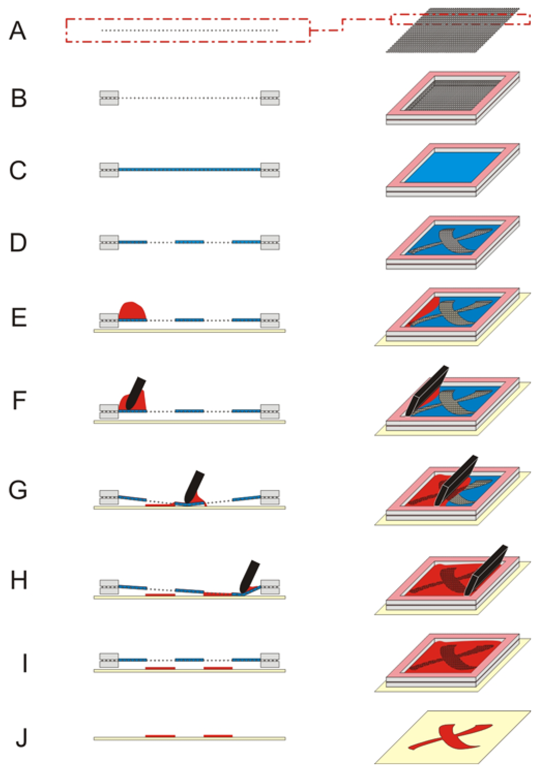
Figure 1.
Fabrication of stencil (A-D) and printing process (E-J). A net made from steel or nylon (A) is mounted in a stiff frame (B) and covered with a photo-curable paint (C). After curing, the negative form of requested pattern creates on the net (D). Ready to use, the stencil is arranged on the top of a substrate to be covered and a paste is put on the stencil (E). Squeegee movement spreads the paste on the whole stencil's surface (F-H). The paste goes through the openings in the stencil and covers the substrate in the requested way (I). Drying the printed pattern (J) finishes the whole process.

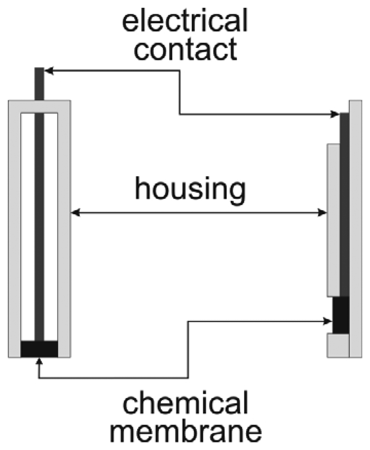
Figure 2.
A conventional ion-selective electrode structure (left) in comparison with a structure of the screen-printed planar sensor (right).
Figure 2.
A conventional ion-selective electrode structure (left) in comparison with a structure of the screen-printed planar sensor (right).

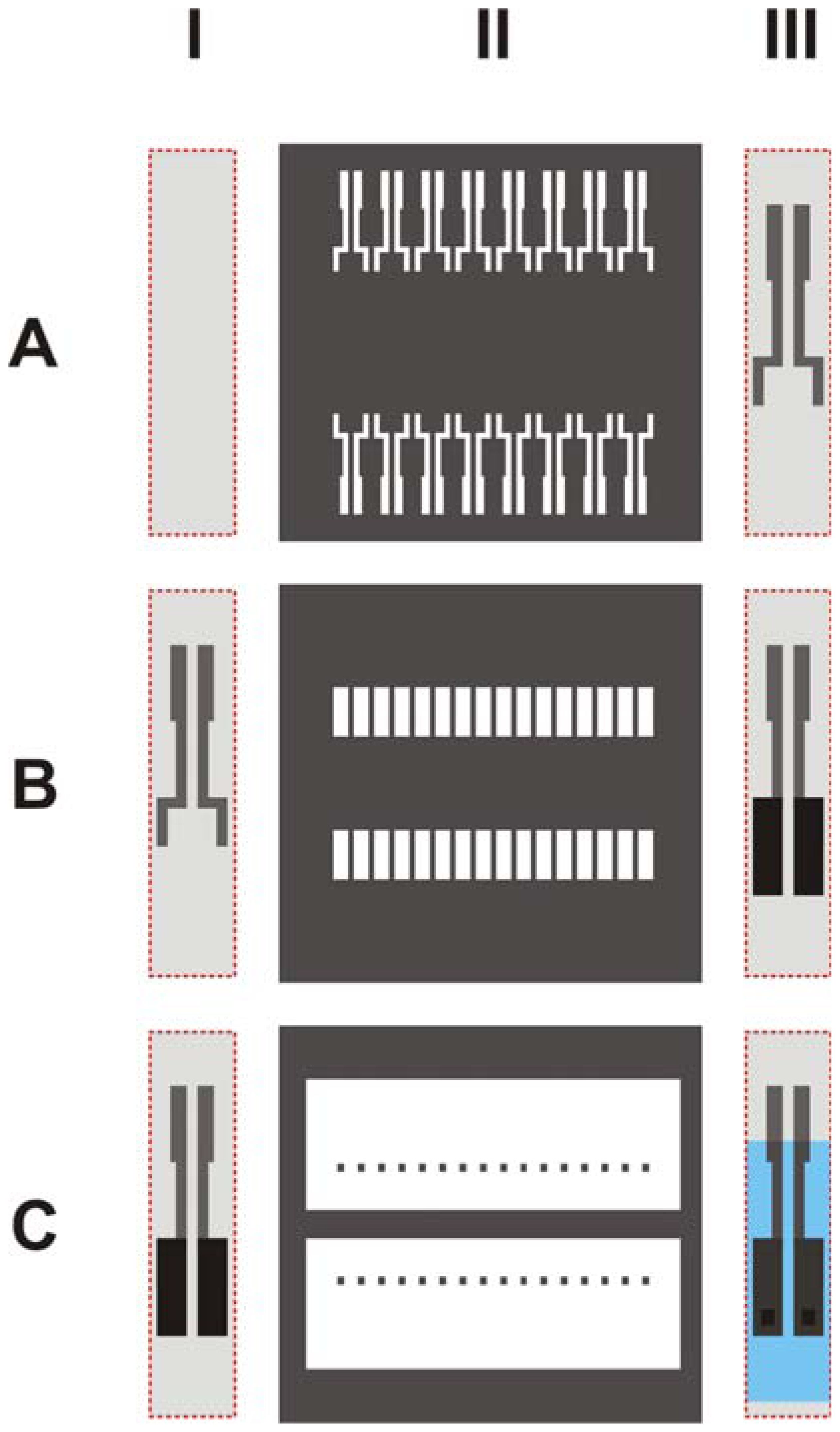
Figure 3.
Schematic view of the patterns (II) used for ion-selective electrodes by screen-printing process. (A) stencil's pattern used for fabrication of electrical contact of sensors, (B) stencil's pattern used for fabrication of chemical membrane of screen-printed electrodes, (C) stencil's pattern used for insulation layer fabrication. I and III are the schematic view of the substrate before and after the printing process.

Figure 4.
Photo of screen-printed sensors and connector compatible to them.
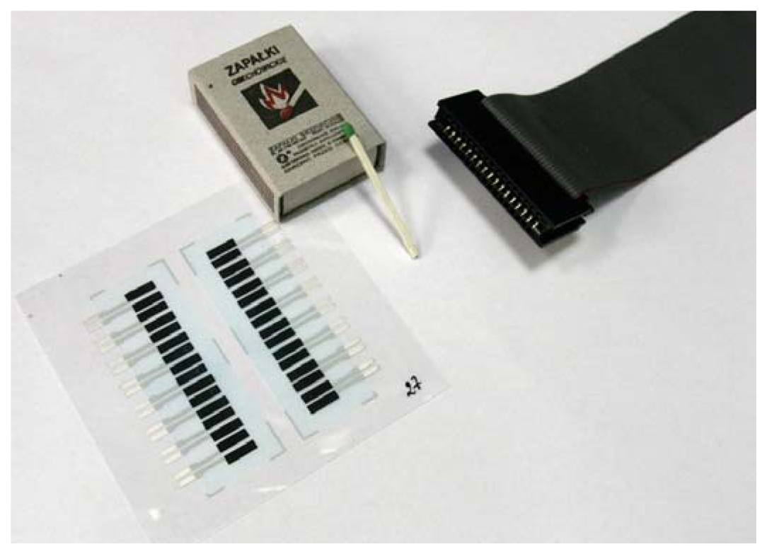
Figure 5.
Typical responses and corresponding calibration graphs of the developed thick-film ion-selective electrodes.
Figure 5.
Typical responses and corresponding calibration graphs of the developed thick-film ion-selective electrodes.
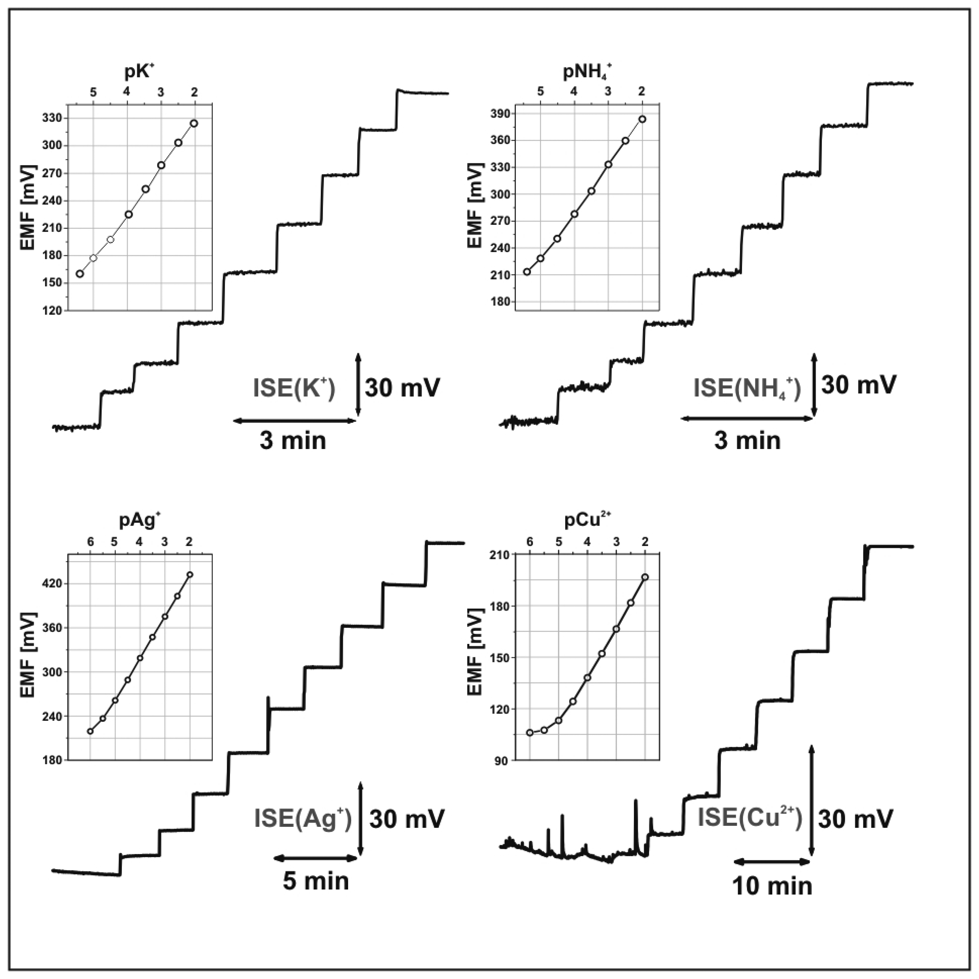
Figure 6.
Structure of a conventional reference electrode of Ag/AgCl/KCl type (left) and design of a planar reference electrode fabricated by means of screen-printing (middle, right). Photo of obtained electrodes with 2 Euro coin (for describing scale) is also shown.
Figure 6.
Structure of a conventional reference electrode of Ag/AgCl/KCl type (left) and design of a planar reference electrode fabricated by means of screen-printing (middle, right). Photo of obtained electrodes with 2 Euro coin (for describing scale) is also shown.
© 2006 by MDPI ( http://www.mdpi.org). Reproduction is permitted for non-commercial purposes.
Share and Cite
MDPI and ACS Style
Tymecki, L.; Glab, S.; Koncki, R. Miniaturized, Planar Ion-selective Electrodes Fabricated by Means of Thick-film Technology. Sensors 2006, 6, 390-396. https://doi.org/10.3390/s6040390
AMA Style
Tymecki L, Glab S, Koncki R. Miniaturized, Planar Ion-selective Electrodes Fabricated by Means of Thick-film Technology. Sensors. 2006; 6(4):390-396. https://doi.org/10.3390/s6040390
Chicago/Turabian StyleTymecki, Lukasz, Stanisław Glab, and Robert Koncki. 2006. "Miniaturized, Planar Ion-selective Electrodes Fabricated by Means of Thick-film Technology" Sensors 6, no. 4: 390-396. https://doi.org/10.3390/s6040390