Fabrication of Au Nanorods by the Oblique Angle Deposition Process for Trace Detection of Methamphetamine with Surface-Enhanced Raman Scattering


Abstract
:1. Introduction
2. Materials and Methods
2.1. Materials
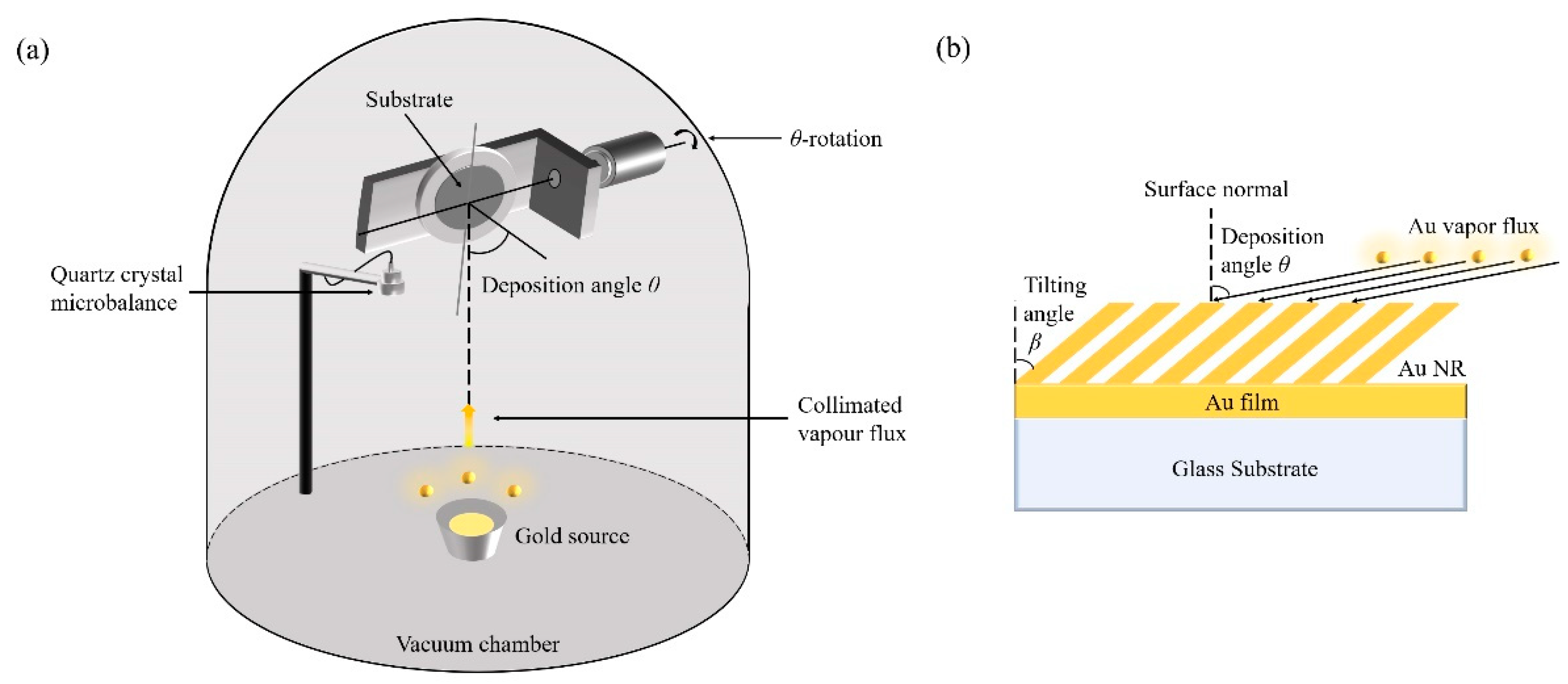
2.2. Apparatus
2.3. FDTD Modeling
2.4. Preparation of AuNRs Substrate
2.5. Raman Measurements
3. Results and Discussion
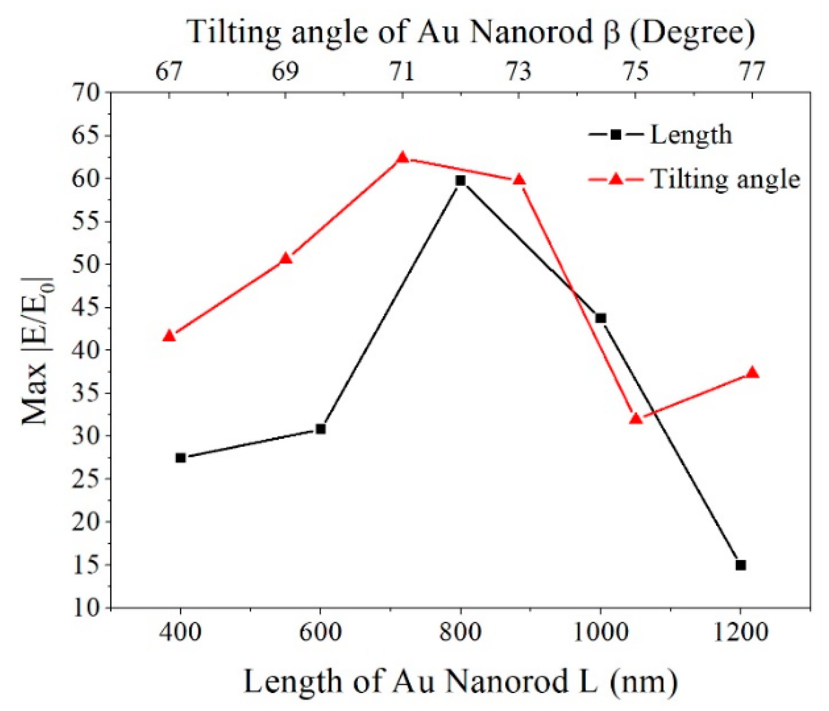
3.1. FDTD Calculation
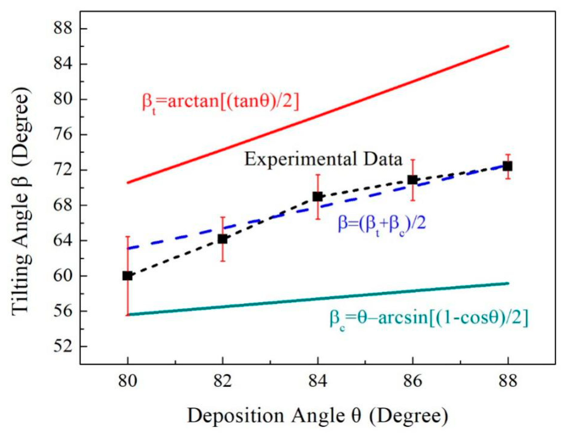
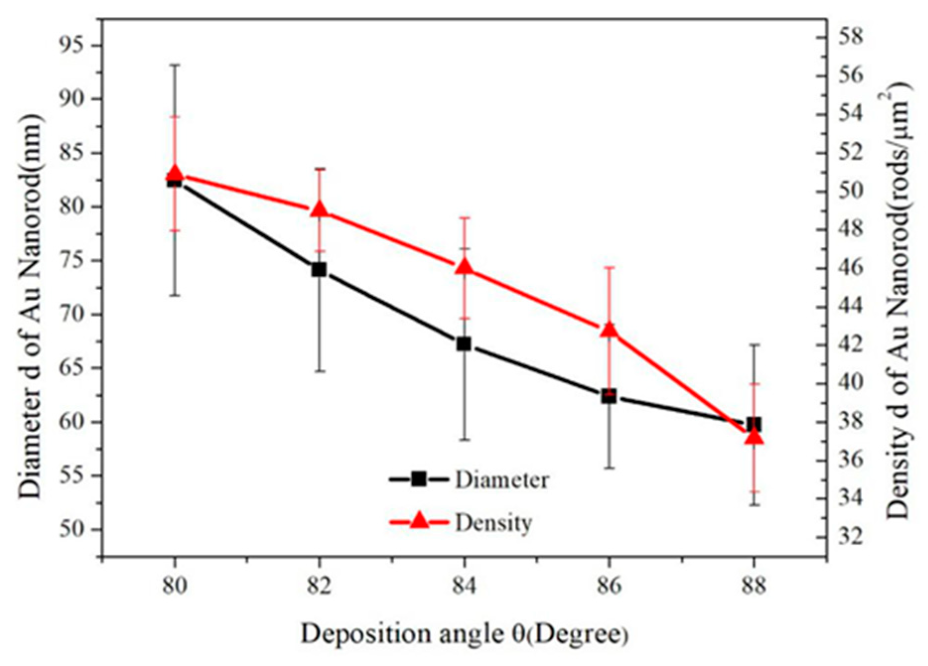
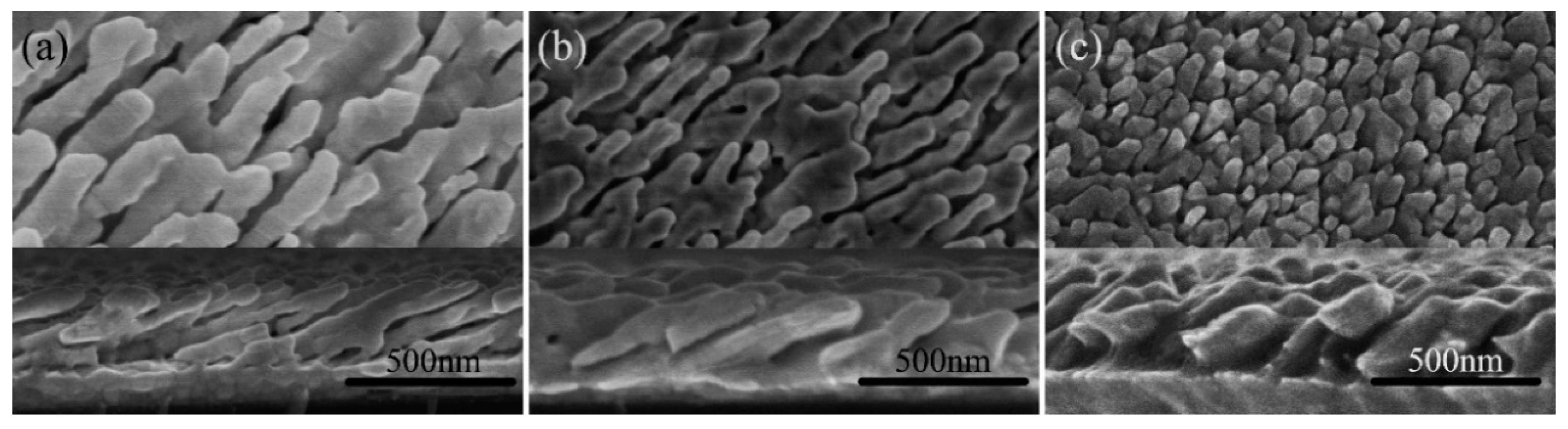
3.2. Morphological Characterizations of Au Nanorod
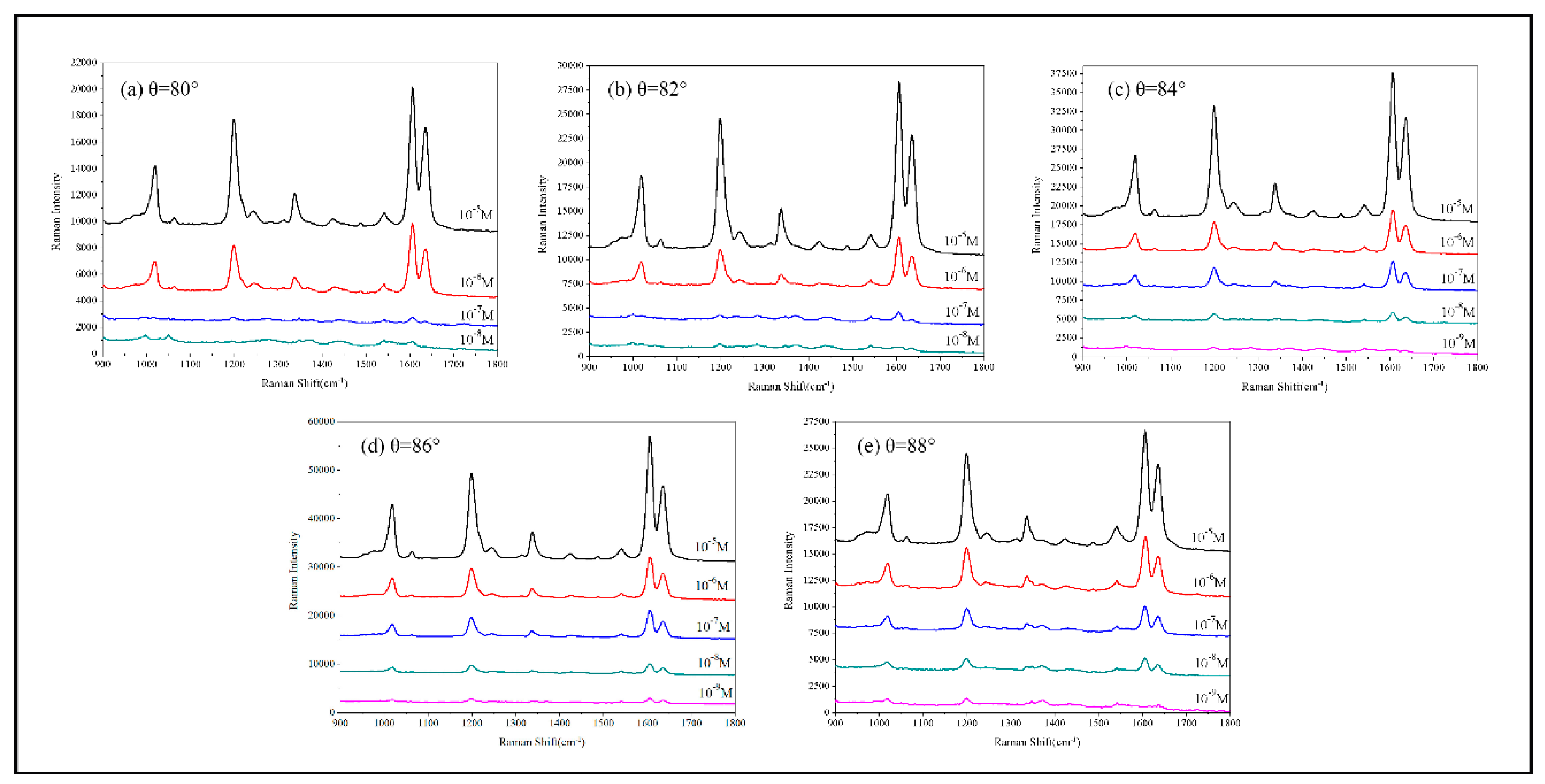
3.3. SERS Performance Characterization
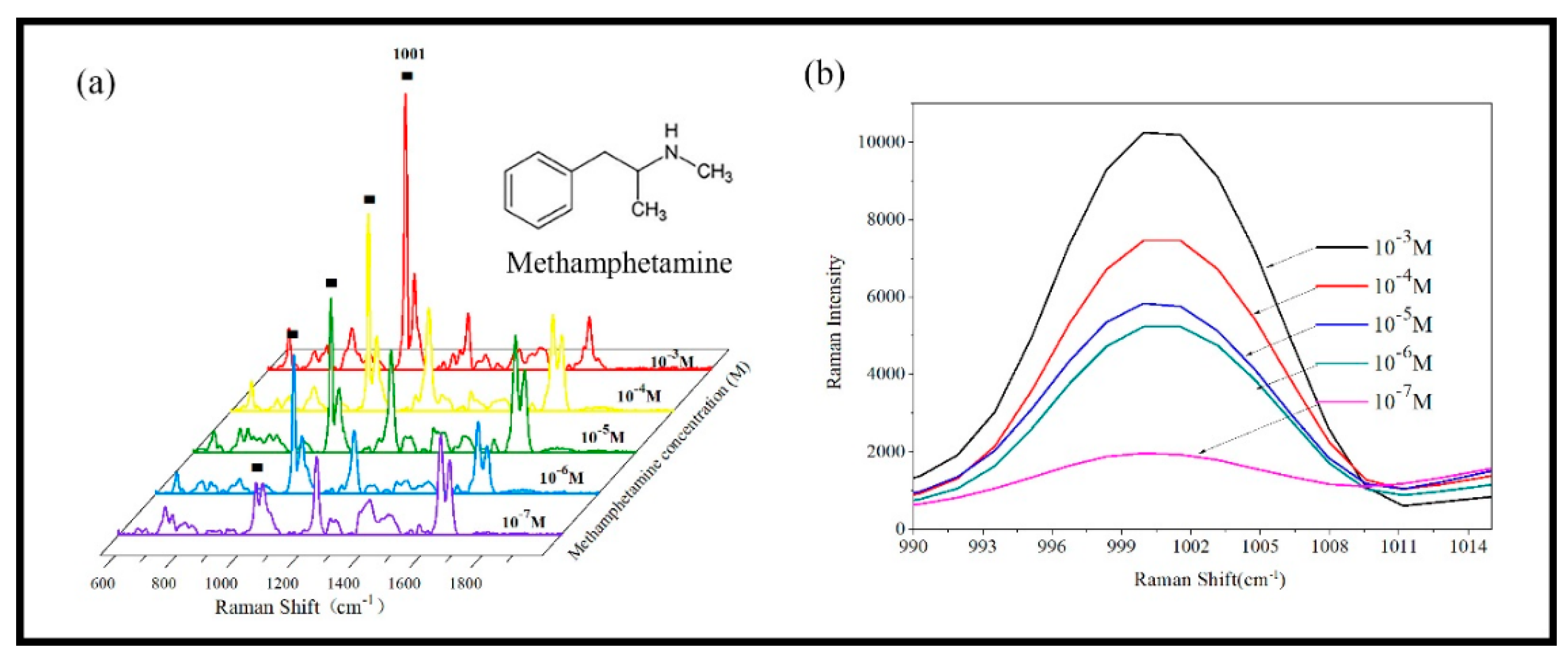
3.4. SERS Detection of Methamphetamine
4. Conclusions
Author Contributions
Funding
Conflicts of Interest
References
- Wang, X.T.; Shi, W.S.; She, G.W.; Mu, L.X.; Lee, S.T. High-performance surface-enhanced Raman scattering sensors based on Ag nanoparticles-coated Si nanowire arrays for quantitative detection of pesticides. Appl. Phys. Lett. 2010, 96, 53104. [Google Scholar] [CrossRef]
- Harper, M.M.; McKeating, K.S.; Faulds, K. Recent developments and future directions in SERS for bioanalysis. Phys. Chem. Chem. Phys. 2013, 15, 5312. [Google Scholar] [CrossRef] [PubMed]
- Feng, Y.; Mo, R.; Wang, L.; Zhou, C.; Hong, P.; Li, C. Surface Enhanced Raman Spectroscopy Detection of Sodium Thiocyanate in Milk Based on the Aggregation of Ag Nanoparticles. Sensors 2019, 19, 1363. [Google Scholar] [CrossRef] [PubMed]
- Zhou, Q.; Zhang, X.; Huang, Y.; Li, Z.; Zhang, Z. Rapid Detection of Polychlorinated Biphenyls at Trace Levels in Real Environmental Samples by Surface-Enhanced Raman Scattering. Sensors 2011, 11, 10851–10858. [Google Scholar] [CrossRef] [PubMed]
- Granger, J.H.; Schlotter, N.E.; Crawford, A.C.; Porter, M.D. Prospects for point-of-care pathogen diagnostics using surface-enhanced Raman scattering (SERS). Chem. Soc. Rev. 2016, 45, 3865–3882. [Google Scholar] [CrossRef]
- Chen, C.; Liu, W.; Tian, S.; Hong, T. Novel Surface-Enhanced Raman Spectroscopy Techniques for DNA, Protein and Drug Detection. Sensors 2019, 19, 1712. [Google Scholar] [CrossRef] [PubMed]
- Panneerselvam, R.; Liu, G.K.; Wang, Y.H.; Liu, J.Y.; Ding, S.Y.; Li, J.F.; Wu, D.Y.; Tian, Z.Q. Surface-enhanced Raman spectroscopy: Bottlenecks and future directions. Chem. Commun. 2017, 54, 10–25. [Google Scholar] [CrossRef]
- Wijesuriya, S.; Burugapalli, K.; Mackay, R.; Ajaezi, G.C.; Balachandran, W. Chemically Roughened Solid Silver: A Simple, Robust and Broadband SERS Substrate. Sensors 2016, 16, 1742. [Google Scholar] [CrossRef]
- Chaney, S.B.; Shanmukh, S.; Dluhy, R.A.; Zhao, Y.-P. Aligned silver nanorod arrays produce high sensitivity surface-enhanced Raman spectroscopy substrates. Appl. Phys. Lett. 2005, 87, 31908. [Google Scholar] [CrossRef] [Green Version]
- Wang, H.-H.; Liu, C.-Y.; Wu, S.-B.; Liu, N.-W.; Peng, C.-Y.; Chan, T.-H.; Hsu, C.-F.; Wang, J.-K.; Wang, Y.-L. Highly Raman-Enhancing Substrates Based on Silver Nanoparticle Arrays with Tunable Sub-10nm Gaps. Adv. Mater. 2006, 18, 491–495. [Google Scholar] [CrossRef]
- Lee, S.J.; Morrill, A.R.; Moskovits, M. Supporting information to Hot spots in silver nanowire bundles for surface-enhanced Raman spectroscopy. J. Am. Chem. Soc. 2006, 128, 2200–2201. [Google Scholar] [CrossRef] [PubMed]
- Huang, Z.; Meng, G.; Huang, Q.; Chen, B.; Zhu, C.; Zhang, Z. Large-area Ag nanorod array substrates for SERS: AAO template-assisted fabrication, functionalization, and application in detection PCBs. J. Raman Spectrosc. 2013, 44, 240–246. [Google Scholar] [CrossRef]
- Dinish, U.S.; Agarwal, A.; Yaw, F.C.; Olivo, M.; Champion, P.M.; Ziegler, L.D. Comparison of the Performance of SERS Substrates Fabricated by Deep UV Lithography and Nanosphere Lithography. AIP Conf. Proc. 2010, 1267, 956. [Google Scholar]
- Yang, H.; Jiang, P. Large-Scale Colloidal Self-Assembly by Doctor Blade Coating. Langmuir 2010, 26, 13173–13182. [Google Scholar] [CrossRef] [PubMed]
- Lin, T.-H.; Linn, N.C.; Tarajano, L.; Jiang, B.; Jiang, P. Electrochemical SERS at Periodic Metallic Nanopyramid Arrays. J. Phys. Chem. C 2009, 113, 1367–1372. [Google Scholar] [CrossRef]
- Rochholz, H.; Bocchio, N.; Kreiter, M. Tuning resonances on crescent-shaped noble-metal nanoparticles. New J. Phys. 2007, 9, 53. [Google Scholar] [CrossRef]
- Hanarp, P.; Käll, M.; Sutherland, D.S. Optical Properties of Short Range Ordered Arrays of Nanometer Gold Disks Prepared by Colloidal Lithography. J. Phys. Chem. B 2003, 107, 5768–5772. [Google Scholar] [CrossRef]
- Wang, C.; Wu, X.; Di, D.; Dong, P.; Xiao, R. Orientation-dependent nanostructure arrays based on anisotropic silicon wet-etching for repeatable surface-enhanced Raman scattering. Nanoscale 2016, 8, 4672–4680. [Google Scholar] [CrossRef]
- Liu, X.; Sun, C.-H.; Linn, N.C.; Jiang, B.; Jiang, P. Wafer-Scale Surface-Enhanced Raman Scattering Substrates with Highly Reproducible Enhancement. J. Phys. Chem. C 2009, 113, 14804–14811. [Google Scholar] [CrossRef]
- Willets, K.A.; Van Duyne, R.P. Localized Surface Plasmon Resonance Spectroscopy and Sensing. Annu. Rev. Phys. Chem. 2006, 58, 267–297. [Google Scholar] [CrossRef]
- Lu, Y.; Liu, G.L.; Kim, J.; Mejia, Y.X.; Lee, L.P. Nanophotonic Crescent Moon Structures with Sharp Edge for Ultrasensitive Biomolecular Detection by Local Electromagnetic Field Enhancement Effect. Nano Lett. 2017, 17, 1648–1654. [Google Scholar] [CrossRef] [PubMed]
- Linn, N.C.; Sun, C.-H.; Arya, A.; Jiang, P.; Jiang, B. Surface-enhanced Raman scattering on periodic metal nanotips with tunable sharpness. Nanotechnology 2009, 20, 225303. [Google Scholar] [CrossRef] [PubMed]
- Zhang, X.; Yonzon, C.R.; Van Duyne, R.P. Nanosphere lithography fabricated plasmonic materials and their applications. J. Mater. Res. 2006, 21, 1083–1092. [Google Scholar] [CrossRef] [Green Version]
- Kosiorek, A.; Kandulski, W.; Glaczynska, H.; Giersig, M. Fabrication of Nanoscale Rings, Dots, and Rods by Combining Shadow Nanosphere Lithography and Annealed Polystyrene Nanosphere Masks. Small 2005, 1, 439–444. [Google Scholar] [CrossRef]
- Fu, C.Y.; Agarwal, A.; Thoniyot, P.; Olivo, M. Glucose sensing using 3D array of reproducible surface enhanced Raman scattering substrates. SPIE NanoSci. Eng. 2009, 7397, 73970. [Google Scholar]
- Kosiorek, A.; Kandulski, W.; Chudzinski, P.; Kempa, K.; Giersig, M. Shadow Nanosphere Lithography: Simulation and Experiment. Nano Lett. 2004, 4, 1359–1363. [Google Scholar] [CrossRef]
- Lai, Y.-C.; Ho, H.-C.; Shih, B.-W.; Tsai, F.-Y.; Hsueh, C.-H. High performance and reusable SERS substrates using Ag/ZnO heterostructure on periodic silicon nanotube substrate. Appl. Surf. Sci. 2018, 439, 852–858. [Google Scholar] [CrossRef]
- Perry, H.; Gopinath, A.; Kaplan, D.L.; Negro, L.D.; Omenetto, F.G. Nano- and Micropatterning of Optically Transparent, Mechanically Robust, Biocompatible Silk Fibroin Films. Adv. Mater. 2008, 20, 3070–3072. [Google Scholar] [CrossRef]
- Gunnarsson, L.; Bjerneld, E.J.; Xu, H.; Petronis, S.; Kasemo, B.; Käll, M. Interparticle coupling effects in nanofabricated substrates for surface-enhanced Raman scattering. Appl. Phys. Lett. 2001, 78, 802–804. [Google Scholar] [CrossRef] [Green Version]
- Brodsky, J.L.; Andrews, D.W. Robust, Reproducible, Recyclable SERS Substrates: Monolayers of Gold NanoStars grafted on glass and coated with a thin silica layer. Nanotechnology 2011, 30, 118917–118940. [Google Scholar]
- Daniels, J.K.; Chumanov, G. Nanoparticle–Mirror Sandwich Substrates for Surface-Enhanced Raman Scattering. J. Phys. Chem. B 2005, 109, 17936–17942. [Google Scholar] [CrossRef] [PubMed]
- Lee, Y.H.; Shi, W.; Lee, H.K.; Jiang, R.; Phang, I.Y.; Cui, Y.; Isa, L.; Yang, Y.; Wang, J.; Li, S.; et al. Nanoscale surface chemistry directs the tunable assembly of silver octahedra into three two-dimensional plasmonic superlattices. Nat. Commun. 2015, 6, 6990. [Google Scholar] [CrossRef] [PubMed]
- Mulvihill, M.; Tao, A.; Benjauthrit, K.; Arnold, J.; Yang, P. Surface-Enhanced Raman Spectroscopy for Trace Arsenic Detection in Contaminated Water. Angew. Chem. Int. Ed. 2008, 47, 6456–6460. [Google Scholar] [CrossRef] [PubMed]
- Ngo, Y.H.; Li, D.; Simon, G.P.; Garnier, G. Effect of cationic polyacrylamides on the aggregation and SERS performance of gold nanoparticles-treated paper. J. Colloid Interface Sci. 2013, 392, 237–246. [Google Scholar] [CrossRef] [PubMed]
- Yap, F.L.; Thoniyot, P.; Krishnan, S.; Krishnamoorthy, S. Nanoparticle Cluster Arrays for High-Performance SERS through Directed Self-Assembly on Flat Substrates and on Optical Fibers. ACS Nano 2012, 6, 2056–2070. [Google Scholar] [CrossRef] [PubMed]
- Zhang, L. Self-assembly Ag nanoparticle monolayer film as SERS Substrate for pesticide detection. Appl. Surf. Sci. 2013, 270, 292–294. [Google Scholar] [CrossRef]
- Zhong, L.-B.; Yin, J.; Zheng, Y.-M.; Liu, Q.; Cheng, X.-X.; Luo, F.-H. Self-Assembly of Au Nanoparticles on PMMA Template as Flexible, Transparent, and Highly Active SERS Substrates. Anal. Chem. 2014, 86, 6262–6267. [Google Scholar] [CrossRef]
- Šubr, M.; Petr, M.; Peksa, V.; Kylián, O.; Hanuš, J.; Procházka, M. Ag Nanorod Arrays for SERS: Aspects of Spectral Reproducibility, Surface Contamination, and Spectral Sensitivity. J. Nanomater. 2015, 2015, 1–7. [Google Scholar] [CrossRef] [Green Version]
- Oh, Y.-J.; Kang, M.; Park, M.; Jeong, K.-H. Engineering hot spots on plasmonic nanopillar arrays for SERS: A review. BioChip J. 2016, 10, 297–309. [Google Scholar] [CrossRef]
- Kumar, S.; Lodhi, D.K.; Goel, P.; Kalyani, N.; Mishra, P.; Singh, J.P. Neeti A facile method for fabrication of buckled PDMS silver nanorod arrays as active 3D SERS cages for bacterial sensing. Chem. Commun. 2015, 51, 12411–12414. [Google Scholar] [CrossRef]
- Liu, Y.-J.; Chu, H.Y.; Zhao, Y.-P. Silver Nanorod Array Substrates Fabricated by Oblique Angle Deposition: Morphological, Optical, and SERS Characterizations. J. Phys. Chem. C 2010, 114, 8176–8183. [Google Scholar] [CrossRef]
- Zhao, Y.-P.; Chaney, S.B.; Shanmukh, S.; Dluhy, R.A. Polarized Surface Enhanced Raman and Absorbance Spectra of Aligned Silver Nanorod Arrays. J. Phys. Chem. B 2006, 110, 3153–3157. [Google Scholar] [CrossRef] [PubMed]
- Blackwell, R.; Zhao, Y.-P. Metal nanoparticle embedded porous thin films prepared by oblique angle coevaporation. J. Vac. Sci. Technol. B Microelectron. Nanometer Struct. 2008, 26, 1344. [Google Scholar] [CrossRef]
- Ma, L.; Huang, Y.; Hou, M.; Xie, Z.; Zhang, Z. Silver Nanorods Wrapped with Ultrathin Al2O3 Layers Exhibiting Excellent SERS Sensitivity and Outstanding SERS Stability. Sci. Rep. 2015, 5, 12890. [Google Scholar] [CrossRef] [PubMed] [Green Version]
- Limnonthakul, P.; Limwichean, S.; Eiamchai, P.; Horprathum, M.; Supati, A.; Nuntawong, N.; Patthanasetakul, V.; Chindaudom, P.; Supatti, A. Vertically Aligned Ag Nanorod Arrays for Trace Cypermethrin Detection. Adv. Mater. Res. 2014, 979, 259–262. [Google Scholar] [CrossRef]
- Beavers, K.R.; Marotta, N.E.; Bottomley, L.A. Thermal Stability of Silver Nanorod Arrays. Chem. Mater. 2010, 22, 2184–2189. [Google Scholar] [CrossRef]
- Chu, H.O.; Song, S.; Li, C.; Gibson, D. Surface Enhanced Raman Scattering Substrates Made by Oblique Angle Deposition: Methods and Applications. Coatings 2017, 7, 26. [Google Scholar] [CrossRef]
- Singh, J.P.; Lanier, T.E.; Zhu, H.; Dennis, W.M.; Tripp, R.A.; Zhao, Y. Highly Sensitive and Transparent Surface Enhanced Raman Scattering Substrates Made by Active Coldly Condensed Ag Nanorod Arrays. J. Phys. Chem. C 2012, 116, 20550–20557. [Google Scholar] [CrossRef]
- Oh, M.-K.; Shin, Y.-S.; Lee, C.-L.; De, R.; Kang, H.; Yu, N.E.; Kim, B.H.; Kim, J.H.; Yang, J.-K. Morphological and SERS Properties of Silver Nanorod Array Films Fabricated by Oblique Thermal Evaporation at Various Substrate Temperatures. Nanoscale Res. Lett. 2015, 10, 737. [Google Scholar] [CrossRef]
- He, Z.; Kretzschmar, I. Template-Assisted GLAD: Approach to Single and Multipatch Patchy Particles with Controlled Patch Shape. Langmuir 2013, 29, 15755–15761. [Google Scholar] [CrossRef]
- Ingram, W.M.; Han, C.; Zhang, Q.; Zhao, Y. Optimization of Ag-Coated Polystyrene Nanosphere Substrates for Quantitative Surface-Enhanced Raman Spectroscopy Analysis. J. Phys. Chem. C 2015, 119, 27639–27648. [Google Scholar] [CrossRef]
- Keating, M.; Song, S.; Wei, G.; Graham, D.; Chen, Y.; Placido, F. Ordered silver and copper nanorod arrays for enhanced Raman scattering created via guided oblique angle deposition on polymer. J. Phys. Chem. C 2014, 118, 4878–4884. [Google Scholar] [CrossRef]
- Stoddart, P.R.; Jayawardhana, S. Nanofabrication of surface-enhanced Raman scattering substrates for optical fiber sensors. Spie Moems-Mems 2013, 8613, 86130. [Google Scholar]
- Suzuki, M.; Nakajima, K.; Kimura, K.; Fukuoka, T.; Mori, Y. Au nanorod arrays tailored for surface-enhanced Raman spectroscopy. Anal. Sci. 2007, 23, 829–833. [Google Scholar] [CrossRef] [PubMed]
- Fan, J.-G.; Zhao, Y.-P. Gold-Coated Nanorod Arrays as Highly Sensitive Substrates for Surface-Enhanced Raman Spectroscopy. Langmuir 2008, 24, 14172–14175. [Google Scholar] [CrossRef] [PubMed]
- Jen, Y.-J.; Chan, S.; Huang, J.-W.; Jheng, C.-Y.; Liu, W.-C. Self-Shadowing Deposited Pure Metal Nanohelix Arrays and SERS Application. Nanoscale Res. Lett. 2015, 10, 247401. [Google Scholar] [CrossRef] [PubMed]
- Jen, Y.-J.; Huang, J.-W.; Liu, W.-C.; Chan, S.; Tseng, C.-H. Glancing angle deposited gold nanohelix arrays on smooth glass as three-dimensional SERS substrates. Opt. Mater. Express 2016, 6, 697. [Google Scholar] [CrossRef]
- Dikovska, A.O.; Avdeev, G.V.; Nedyalkov, N.N.; Koleva, M.E.; Atanasov, P.A. Preparation of metal nanorods substrates for SERS application. In Proceedings of the Seventeenth International School on Quantum Electronics: Laser Physics and Applications, Nessebar, Bulgaria, 24–28 September 2012; Volume 8770, p. 877006. [Google Scholar]
- Tang, X.; Zhao, Y.; Dluhy, R.A. The use of aligned silver nanorod arrays prepared by oblique angle deposition as surface enhanced Raman scattering substrates. J. Phys. Chem. C 2008, 112, 895–901. [Google Scholar]
- Liu, Y.-J.; Zhao, Y.-P. Simple model for surface-enhanced Raman scattering from tilted silver nanorod array substrates. Phys. Rev. B 2008, 78, 1–9. [Google Scholar] [CrossRef]
- Meyer, M.R.; Wilhelm, J.; Peters, F.T.; Maurer, H.H. Beta-keto amphetamines: Studies on the metabolism of the designer drug mephedrone and toxicological detection of mephedrone, butylone, and methylone in urine using gas chromatography–mass spectrometry. Anal. Bioanal. Chem. 2010, 397, 1225–1233. [Google Scholar] [CrossRef]
- Mahoor, N.; Tehrani, M.S.; Givianrad, M.H. Surfactant-assisted dispersive liquid–liquid microextraction followed by high-performance liquid chromatography for determination of amphetamine and methamphetamine in urine samples. Anal. Methods 2012, 4, 1357. [Google Scholar]
- Chen, X. Simultaneous determination of four designer drugs and their major metabolites by liquid chromatography–mass spectrometry. J. Chromatogr. B 2015, 992, 1–7. [Google Scholar] [CrossRef] [PubMed]
- Nadulski, T. Utility of ELISA screening for the monitoring of abstinence from illegal and legal drugs in hair and urine. Drug Test. Anal. 2014, 6, 101–109. [Google Scholar]
- Van Der Heide, S.; Russell, D.A. Optimisation of immuno-gold nanoparticle complexes for antigen detection. J. Colloid Interface Sci. 2016, 471, 127–135. [Google Scholar] [CrossRef] [PubMed]
- Hawkeye, M.M.; Taschuk, M.T.; Brett, M.J. Glancing Angle Deposition of Thin Films: Engineering the Nanoscale; John Wiley & Sons: Hoboken, NJ, USA, 2014; ISBN 9781118847565. [Google Scholar]
- Sikkens, M.; Horowitz, F.; Hodgkinson, I.J.; Macleod, H.A.; Wharton, J.J. Measurement of the principal refractive indices of thin films deposited at oblique incidence. J. Opt. Soc. Am. A 2008, 2, 1693. [Google Scholar]
- Lee, J.; Min, K.; Kim, Y.; Yu, H.K.; Ag, A. Surface-Enhanced Raman Spectroscopy (SERS) Study Using Oblique Angle Deposition of Ag Using Different Substrates. Materials 2019, 12, 1581. [Google Scholar] [CrossRef]
- Chen, J.; Dong, P.; Wang, C.; Zhang, C.; Wang, J.; Wu, X. Performance Improving Method of Aligned Silver Nanorod by Grafting Au@Ag Core–Shell Nanoparticles for Surface-Enhanced Raman Scattering. Nano 2017, 12, 1750131. [Google Scholar] [CrossRef]
- Le Ru, E.C.; Blackie, E.; Meyer, M.; Etchegoin, P.G. Surface Enhanced Raman Scattering Enhancement Factors: A Comprehensive Study. J. Phys. Chem. C 2007, 111, 13794–13803. [Google Scholar] [CrossRef]
- Han, C.; Yao, Y.; Wang, W.; Qu, L.; Bradley, L.; Sun, S.; Zhao, Y. Rapid and sensitive detection of sodium saccharin in soft drinks by silver nanorod array SERS substrates. Sens. Actuators B Chem. 2017, 251, 272–279. [Google Scholar] [CrossRef]
- Ma, Y.; Liu, H.; Mao, M.; Meng, J.; Yang, L.; Liu, J. Surface-Enhanced Raman Spectroscopy on Liquid Interfacial Nanoparticle Arrays for Multiplex Detecting Drugs in Urine. Anal. Chem. 2016, 88, 8145–8151. [Google Scholar] [CrossRef] [PubMed]
- Muehlethaler, C.; Leona, M.; Lombardi, J.R. Towards a validation of surface-enhanced Raman scattering (SERS) for use in forensic science: Repeatability and reproducibility experiments. Forensic Sci. Int. 2016, 268, 1–13. [Google Scholar] [CrossRef] [PubMed]


| Method | SERS Performance | Repeatability | Uniformity | Substrate Area | Preparation Time | Preparation Cost |
|---|---|---|---|---|---|---|
| AAO [10,11,12] | high | good | good | wafer-level | short | lower |
| NSL [13,14,15,16,17,18,19,20,21,22,23,24,25,26] | higher | good | good | wafer-level | short | lower |
| EBL [27,28,29] | high | best | best | small | long | high |
| Self-Assembly [30,31,32,33,34,35,36,37] | high | best | best | wafer-level | short | low |
| OAD [38,39,40] | higher | best | best | wafer-level | shorter | lower |
| Wavenumber (cm−1) | Assignments of SERS Bands |
|---|---|
| 1198 | C-C Stretch |
| 1605 | Aromatic ring stretching |
| 1637 | in-plane ring |
| Assignments of SERS Bands | Literature Report Wavenumber [72,73] (cm−1) | Experimental Data (cm−1) |
|---|---|---|
| the breathing vibration of the benzene ring | 620 | 618 |
| the stretching vibration mode of isopropyl C-C | 834 | 835 |
| the breathing vibration of the benzene ring | 1001 | 1001 |
| the breathing vibration of the benzene ring | 1023 | 1027 |
| the phenyl-C stretching mode | 1207 | 1204 |
| the phenyl-C stretching mode | 1212 | |
| the stretching of benzene ring | 1583 | 1580 |
| the stretching of benzene ring | 1601 | 1605 |
© 2019 by the authors. Licensee MDPI, Basel, Switzerland. This article is an open access article distributed under the terms and conditions of the Creative Commons Attribution (CC BY) license (http://creativecommons.org/licenses/by/4.0/).
Share and Cite
Li, B.; Wang, T.; Su, Q.; Wu, X.; Dong, P. Fabrication of Au Nanorods by the Oblique Angle Deposition Process for Trace Detection of Methamphetamine with Surface-Enhanced Raman Scattering. Sensors 2019, 19, 3742. https://doi.org/10.3390/s19173742
Li B, Wang T, Su Q, Wu X, Dong P. Fabrication of Au Nanorods by the Oblique Angle Deposition Process for Trace Detection of Methamphetamine with Surface-Enhanced Raman Scattering. Sensors. 2019; 19(17):3742. https://doi.org/10.3390/s19173742
Chicago/Turabian StyleLi, Baini, Tianran Wang, Qingqing Su, Xuezhong Wu, and Peitao Dong. 2019. "Fabrication of Au Nanorods by the Oblique Angle Deposition Process for Trace Detection of Methamphetamine with Surface-Enhanced Raman Scattering" Sensors 19, no. 17: 3742. https://doi.org/10.3390/s19173742