1. Introduction
CMOS image sensors with global shutter (GS) are becoming popular [
1,
2,
3]. It is possible to capture the shape of a high speed moving object with high accuracy without distortion. Conventional CMOS sensors adopt rolling shutter (RS) method. In the RS method, an exposure is sequentially performed for each row pixel and there is a slight time difference in signal readout for each row pixel. Thus, the high-speed moving object is distorted. For example, when a flash is used during shooting, the flash band phenomenon may occur with different brightness of the image on the top and the bottom. CMOS image sensor with GS exposes all the pixels at the same time and it can take a non-distorted photograph of the high speed moving object such as a rotating propeller. Therefore, it is expected to be utilized in the automotive field and industrial applications such as inspection cameras.
GS CMOS image sensor with small pixel is demanded for high resolution pictures and sensing. In practical use of GS sensor, it is important to achieve high signal-to-noise ratio. High quantum efficiency (QE) is required to increase the signal intensity. In order to increase the QE, it is necessary to provide more light to the photo diode (PD) even in small size pixel. In terms of noise, it is necessary to care the noise caused by GS structure.
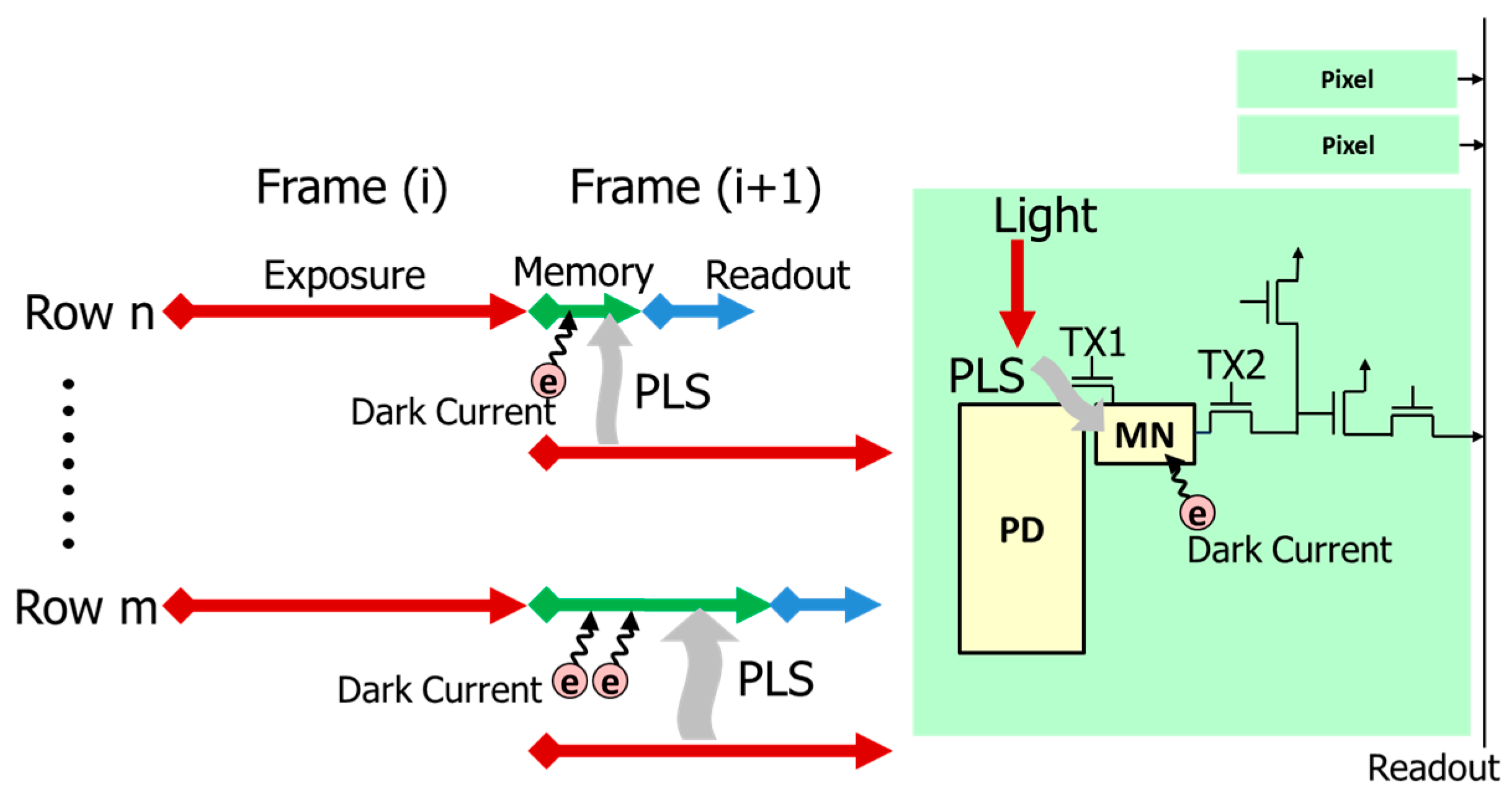
Figure 1 shows a simple configuration and reading method of GS pixel. In order to realize GS capability, a memory node (MN) must be added in each pixel [
4]. The electrons stored in the PD are collectively read out to MN and used as an image signal. The exposure is performed at once, but the readout is performed for each row as shown in
Figure 1. Therefore, the electrons are generated in the MN before the readout becomes noise, and leads to deterioration in image quality. When an image is output with much noise, the lower part of the picture becomes brighter or noisy because the noise is increased in later read rows. Accordingly, it is necessary to reduce the noise generated in the MN. Major causes of the noise are light penetration into MN and dark current.
PLS is generated by light incident into MN. An increase of PLS leads to deterioration of image quality. This is because the charges generated by incident light to MN are added to the charges stored in MN after the exposure. In this paper, we present the advanced approach of optical design in 2.8 μm GS pixel for drastic improvement of PLS and QE [
5]. We expand our original paper with a new storage-gate based MN for low dark current.
Figure 2 shows a schematic and potential diagram of storage-gate based MN. For small GS pixel, dual transfer GS pixels are suitable from the point of views of scalability, low read noise, and low dark current. Their fewer components in pixels offer a better scalability compared to 8T voltage domain pixels [
6].
In dual transfer GS pixels, the photo-generated charges are transferred to MN. This allows a correlated double sampling (CDS) on a floating diffusion in successive transfer, which can reduce pixel noise to below 1 to 2 electrons [
7,
8]. This read noise is much better than that of 5T charge transfer pixels without CDS [
1]. Additionally, such MN shows much smaller dark current compared to floating diffusion used as MN in 5T-GS pixels [
9]. Considering the MN in dual transfer GS pixels, pinned MN and storage-gate based MN were reported [
8,
9]. In the storage-gate based MN shown in
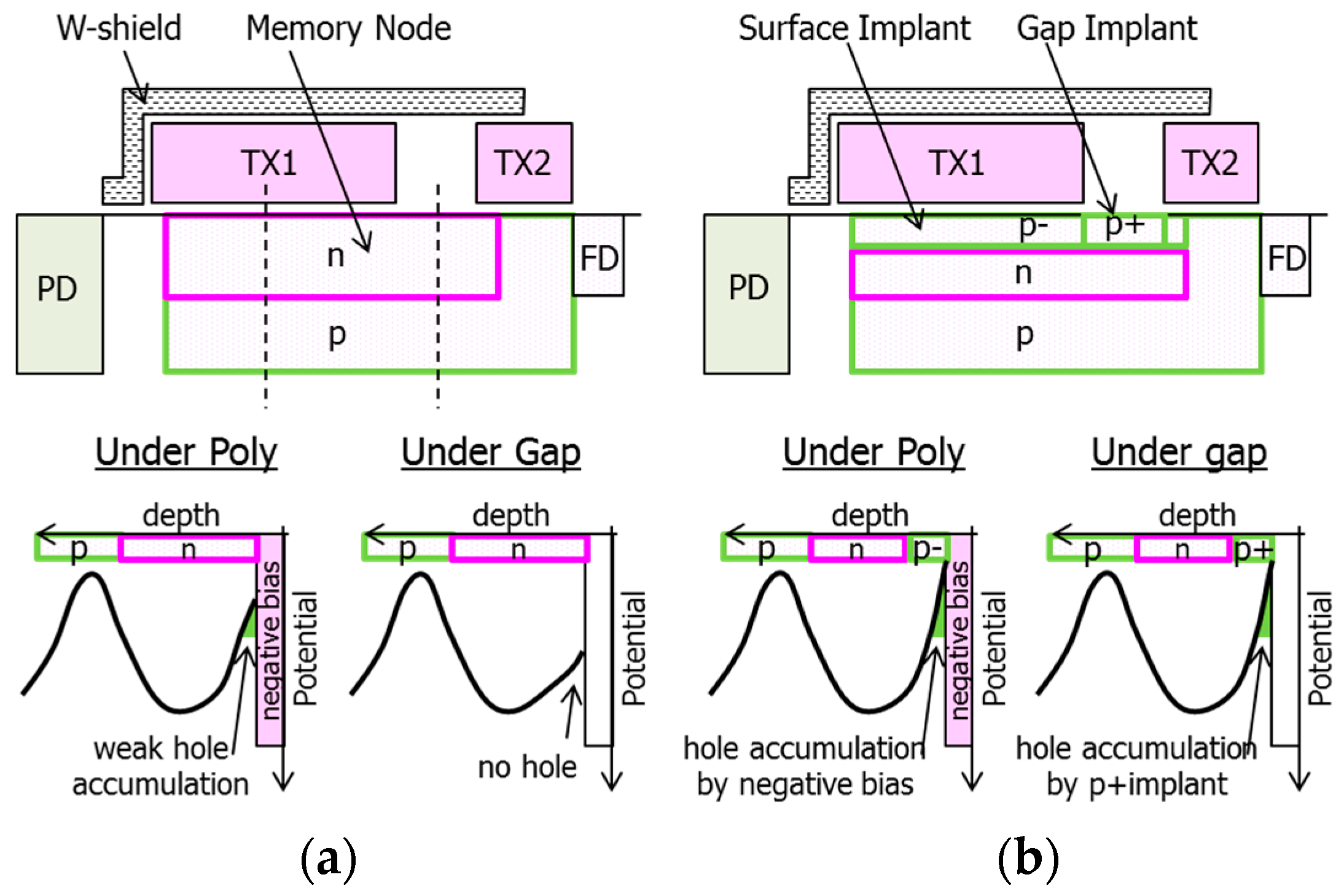
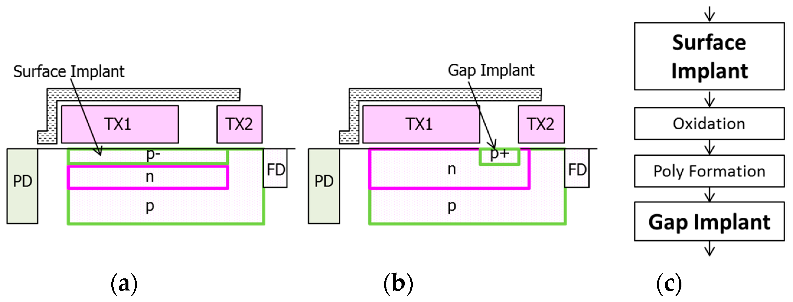
Figure 2, the storage-gate can control the depletion potential of the MN. This offers better charge transfer from the PD to the MN. Furthermore, using a single poly-Si gate on MN for both transfer and storage can enlarge its gate area, and it can enhance potential controllability. It makes the storage-gate based MN suitable for small GS pixels. Although the reported dark current of storage-gate based MN is higher than that of the pinned MN due to dark current generation at the surface of MN [
8], its potential controllability can also improve dark current in combination with negative gate biasing.
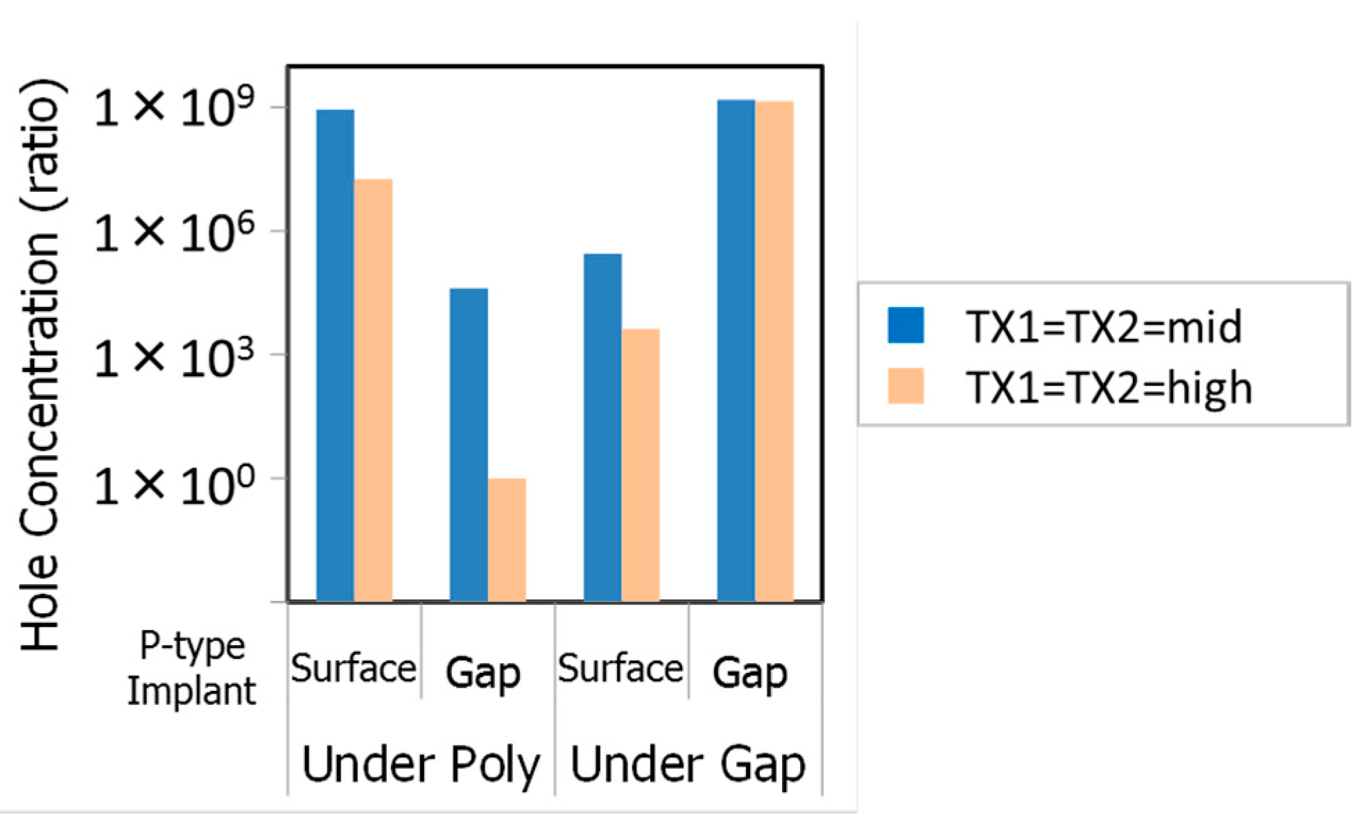
This paper reports on newly developed storage-gate based MN structures to suppress dark current with negative gate biasing and surface p-type implants. The generation position of dark current identified by the test structures is also described.
2. Device Structure
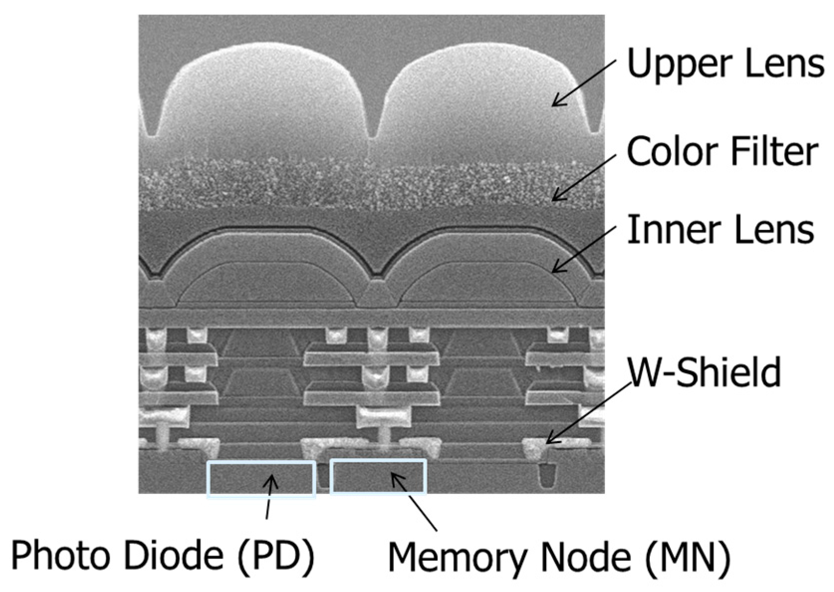
Figure 3 shows the cross-section of global shutter pixel structure we developed. The pixel was designed with 110 nm node process, including double micro lens, three-layer Cu wiring and tungsten (W) light shield structures. The incident light is collected by the upper lens and the inner lens, then passes between the Cu-wirings, and finally enters the PD. The MN is placed next to the PD. W light shield is placed just above the MN to block an incident light as shown in
Figure 3 [
10,
11].
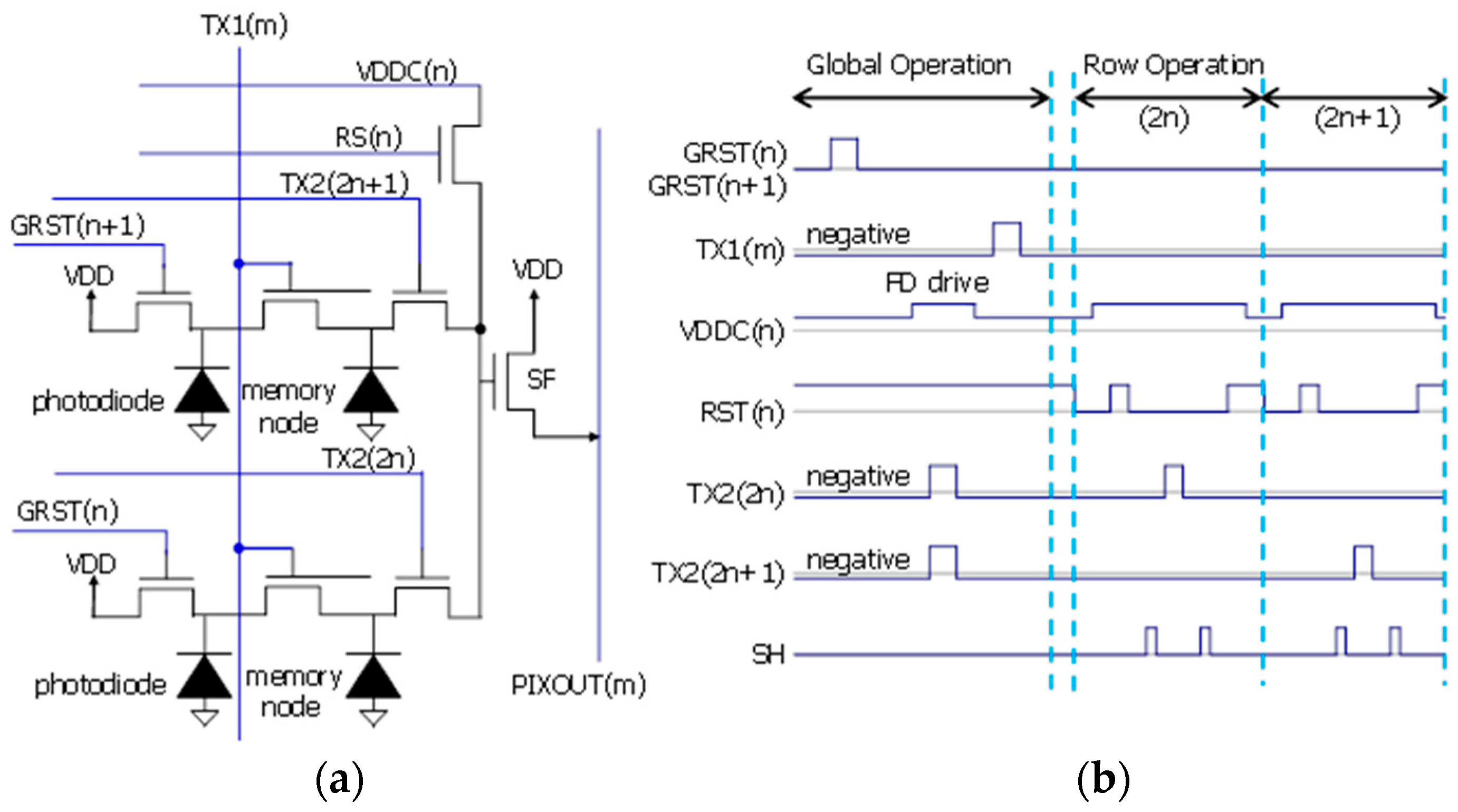
Figure 4a shows a schematic diagram of pixel circuit and
Figure 4b shows a timing diagram. In order to increase the PD area and MN area, we use a 2 × 1 sharing scheme. The pixel has no row-select and the floating diffusion drive method is used [
12]. TX1 is served as a control line for both a transfer gate from the PD to MN and a storage-gate over MN to reduce a control line for the storage-gate. During operation, except for transferring electron from PD to MN, TX1 and TX2 biases are kept negative for suppressing dark current, where accumulated holes at the surface occupy recombination centers and prevent carrier generation [
9].
3. Reduction of PLS
3.1. Structural Issue of Small GS Pixels in PLS Reduction
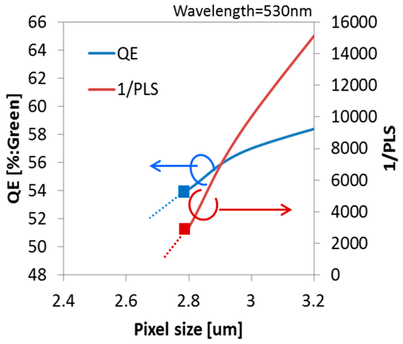
In order to reduce PLS, it is necessary to reduce the incident light to MN.
Figure 5 shows the pixel size dependence of QE and 1/PLS. These data were estimated by optical simulations. Simulation was carried out at the green pixel (wavelength = 530 nm). As the pixel size becomes smaller, QE and 1/PLS are seriously degraded. The degradation of these optical characteristics is due to the fact that the incident light is not concentrated efficiently in the optical aperture. It is not easy to change the wiring width and height in order to keep wiring resistance and capacitance even if the pixel size is scaled down. Therefore, the optical aperture size becomes smaller and it becomes difficult to pass the light between Cu-wirings in small pixels. In this paper, we present the advanced approach of optical design in 2.8 μm GS pixel for drastic improvement of PLS and QE.
It is conceivable to expand the W light shield to prevent light incident on the MN. However, the QE decreases when the W light shield is expanded. It is difficult to realize both high QE and high 1/PLS by simply adjusting the W light shield extension. It is important to improve the optical characteristics by changing the propagation of light.
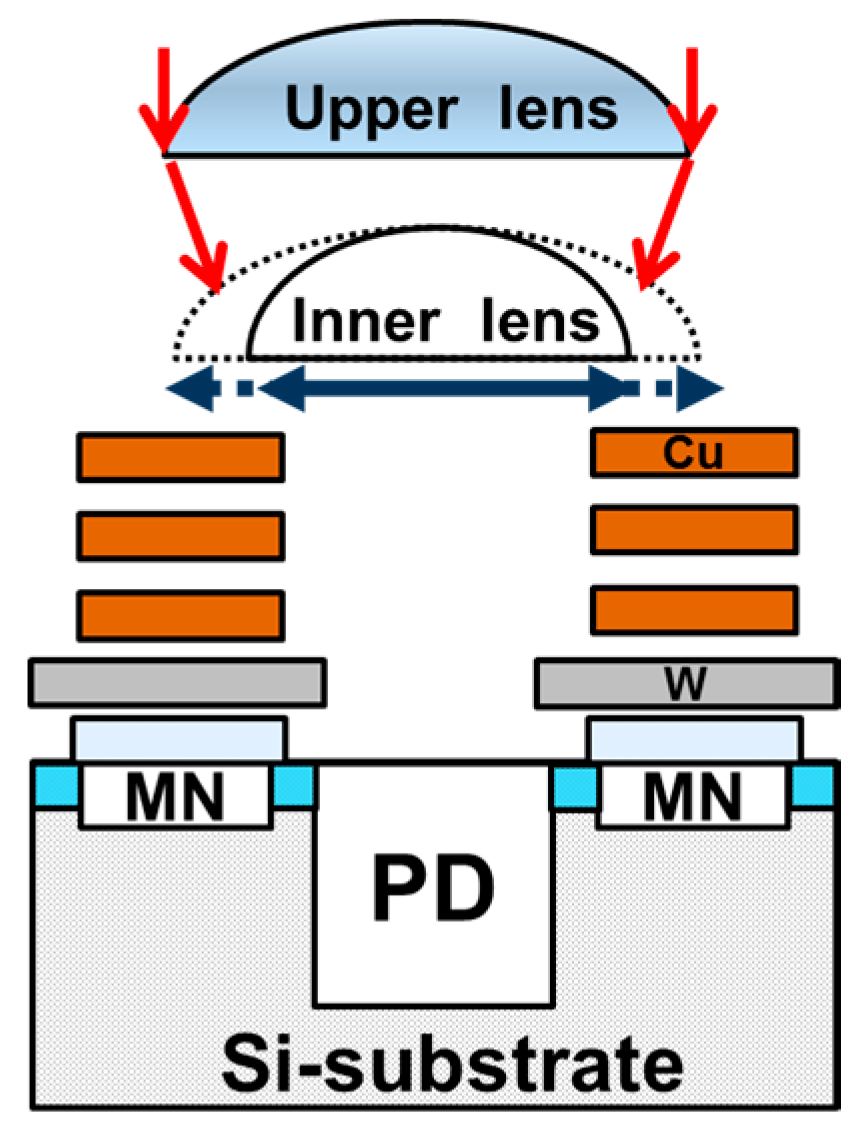
3.2. Effect of Double Micro Lens Structure
A double micro lens structure is often used as a method for efficient light collection into a narrow optical aperture [
13,
14]. An inner lens is placed above the Cu-wiring layers as shown in
Figure 3. In the case of double lens structure, it is possible to adjust the light collection at two positions of the upper lens and the inner lens. It is expected that the light collected by the upper lens can be efficiently collected into the optical aperture.
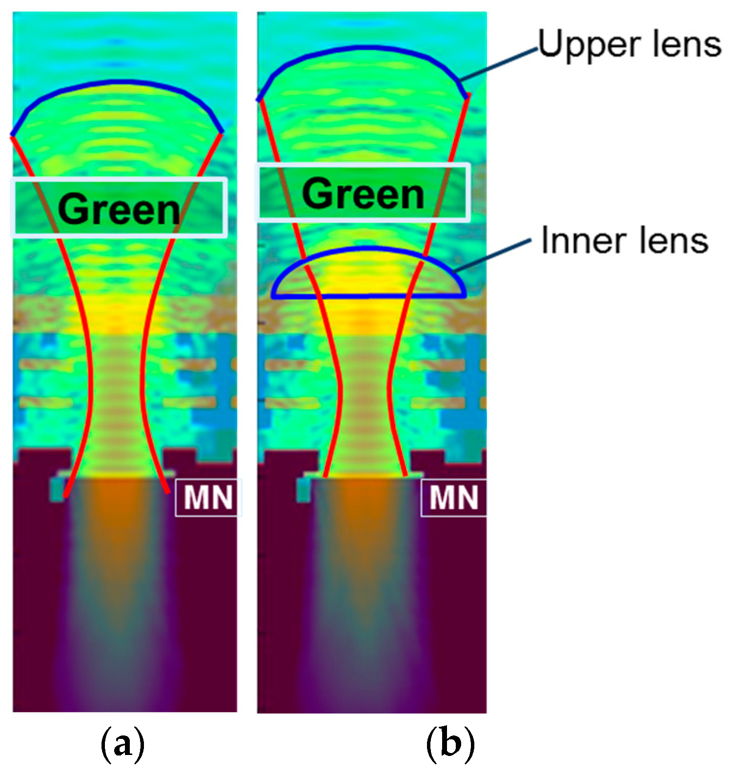
We compared PLS and QE between with and without inner lens structures by optical simulation using three-dimensional finite difference time domain (FDTD) method.
Figure 6 shows the electric field distribution, and
Table 1 shows the simulation results. By adopting inner lens, the incident light was concentrated efficiently in the optical aperture as shown in
Figure 6b. As a result, QE was improved from 54.1% to 58.9%, and 1/PLS was improved by 30%. From the above results, we decided to adopt the double lens structure. For further improvement, we studied the inner lens structure in more detail.
3.3. Analysis and Design Concept of Inner Lens (Our Proposal)
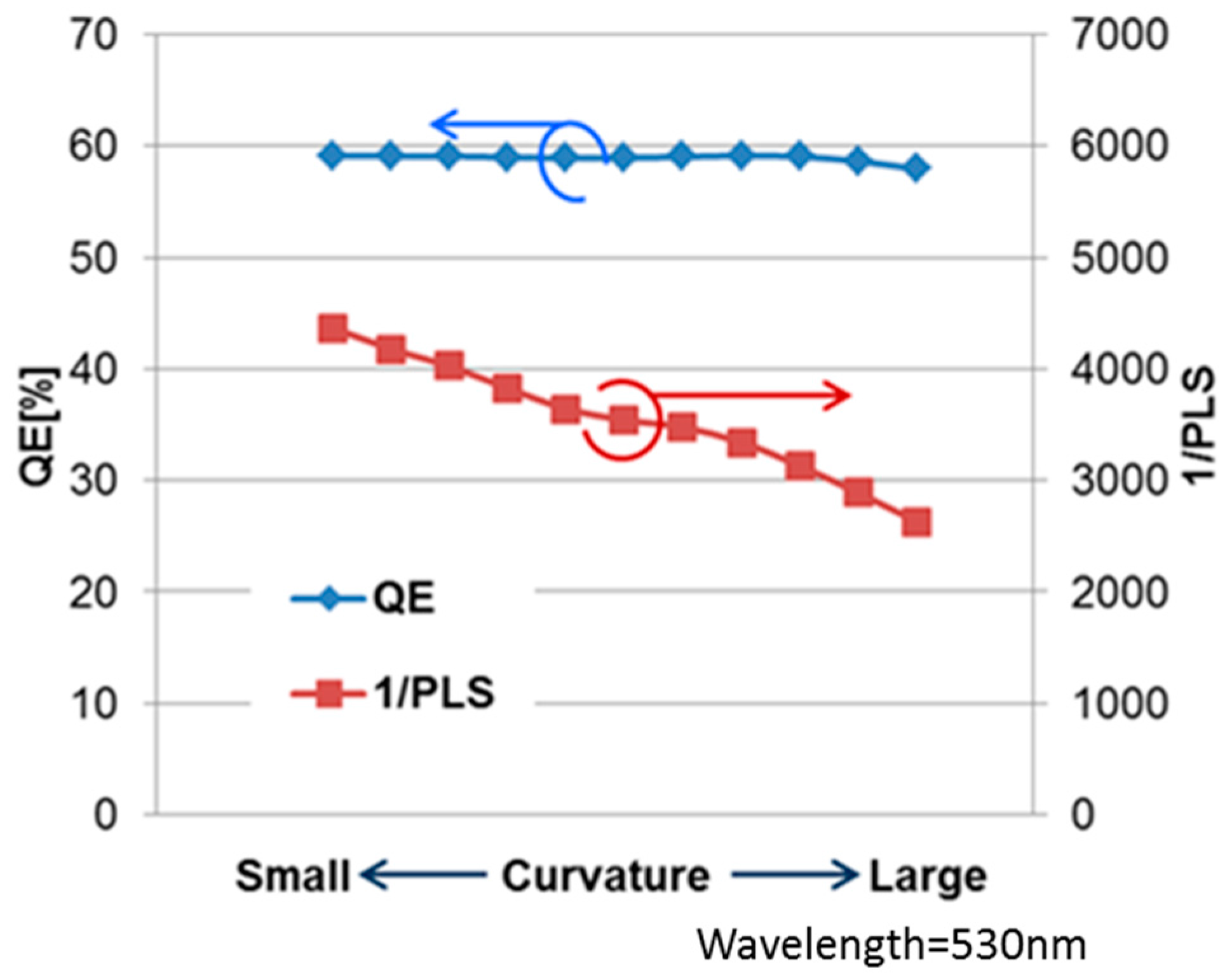
We analyzed the inner lens curvature dependence of QE and PLS by optical simulation.
Figure 7 shows the simulation results. These data were calculated by changing a diameter of inner lens (constant lens height) as shown in
Figure 8.
PLS depends on curvature, and small curvature was better for PLS. On the other hand, QE was stable in the curvature range. It indicates that once the incident light collected by the upper lens enters the inner lens, the light reaches the PD regardless of the inner lens curvature. Therefore, the design concept of the upper lens is to concentrate the light on the inner lens. On the other hand, 1/PLS depends on curvature, and small curvature was better for 1/PLS.
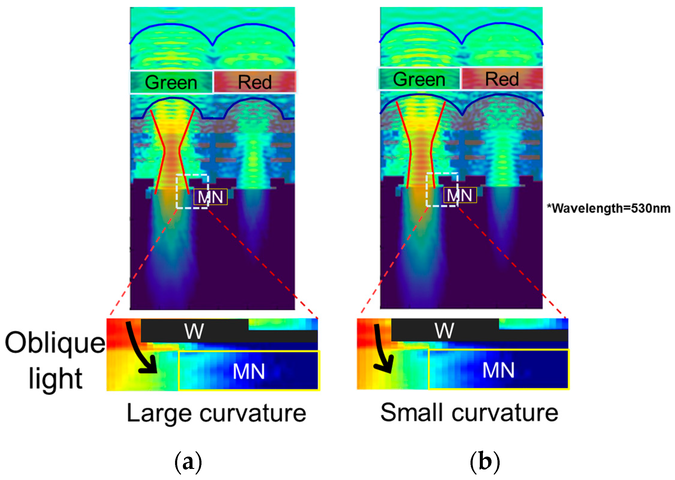
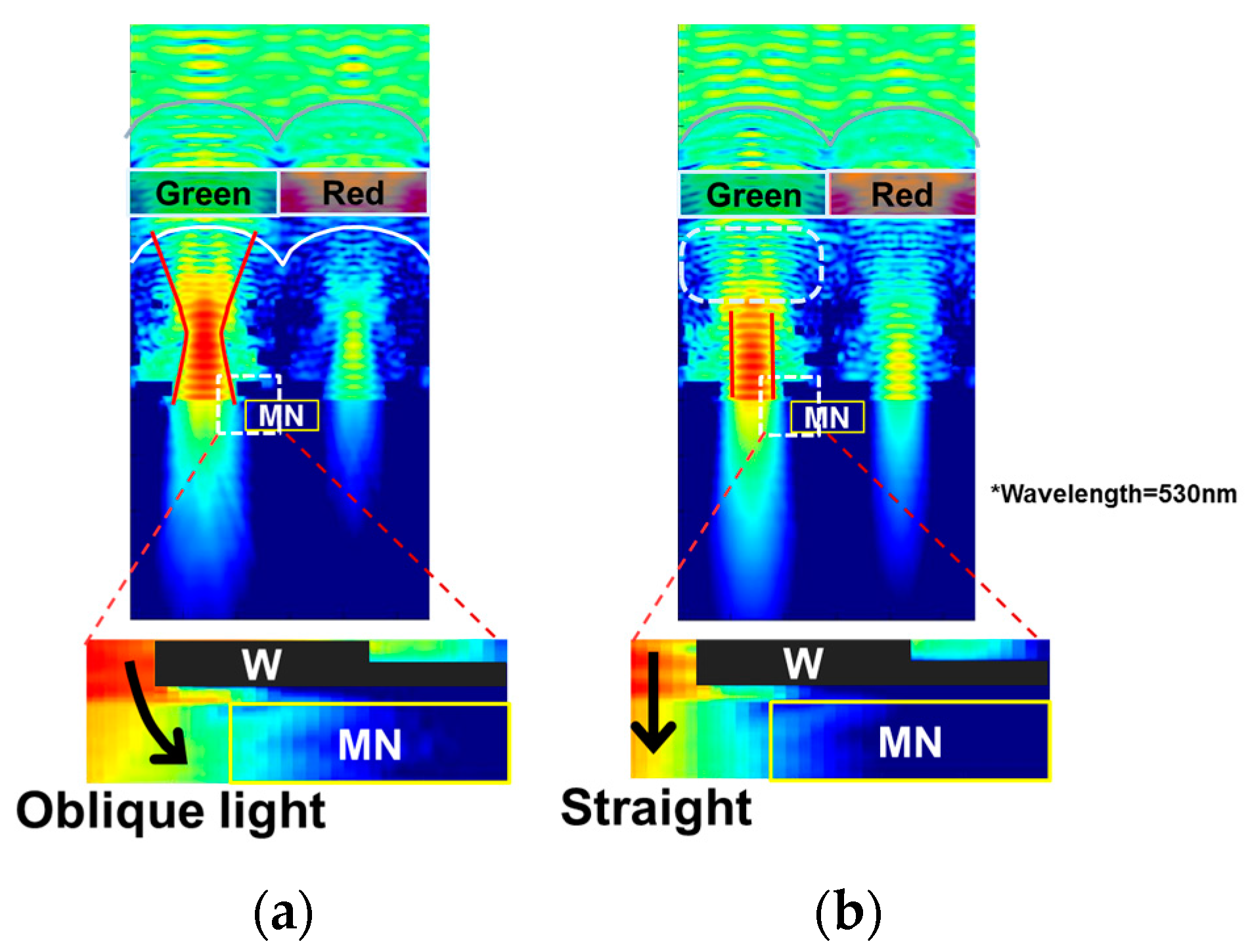
We compared the electric field between large and small curvature to analyze the key factor of PLS.
Figure 9a,b shows the cross-section of electric field distribution. When the inner lens has a large curvature, the beam widely spreads near the W light shield as shown in
Figure 9a. In the case of small curvature lens, the beam spread is narrower than that of large curvature lens. Then the beam enters almost perpendicularly to Si as shown in
Figure 9b.
We analyzed the electric field distribution near the MN in more detail. The bottom views of
Figure 9a,b are the enlarged views of the broken line portion of upper figures. In the case of large curvature inner lens, a large amount of oblique light bent by the inner lens enters the MN as shown in
Figure 9a. On the other hand, in the case of small curvature lens, the light entering the MN decreases as shown in
Figure 9b.
These analyses show it is important to make the light incident perpendicular to Si in order to reduce oblique incidence to the MN. To summarize the results, the double lens design concept is as follows. The incident light collected by the upper lens should be concentrated on the inner lens in order to improve the QE, and the inner lens should be designed so that light enters straight into the Si.
We developed the new inner lens based on this concept.
Figure 10 shows the comparison of electric fields between conventional and newly developed inner lenses. In the case of the newly developed inner lens, we can see that the light enters straight into the silicon as shown in
Figure 10b. The incident light to the MN is greatly reduced. Therefore, the simulated value of 1/PLS is greatly improved and is expected to be 7100.
3.4. Results of Newly Developed Inner Lens Based on Our Design Concept for Low PLS
We fabricated two types of 2.8 μm GS devices with conventional and newly developed inner lenses.
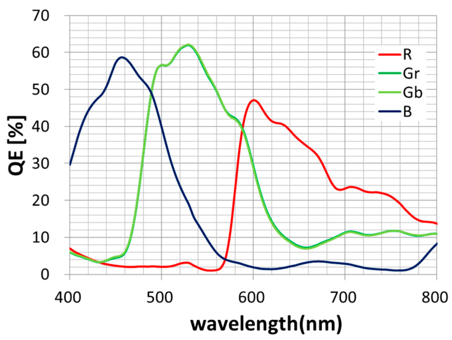
Table 2 shows the measurement results. We confirmed the superiority of the new inner lens based on our concept. The simulation results agreed with the experimental results. The QE of green pixel is the same—62%—in both types. The inner lens developed with the new concept obtained two times better 1/PLS than a conventional lens and the value is 7700. The 1/PLSs of blue and red pixels are 3600 and 2600 (wavelength = 450 nm and 600 nm), respectively.
Figure 11 shows the QE curves with the newly developed inner lens. The QE of blue and red pixels are 59% and 48%, respectively.
5. Conclusions
We developed a low PLS and low dark current 2.8 μm GS pixel. We proposed a new lens design concept for low PLS. The double lens structure was adopted. The double lens design concept we proposed is as follows:
- (1)
The incident light collected by the upper lens should be concentrated on the inner lens in order to improve the QE.
- (2)
The inner lens should be designed so that light enters straight into the Si.
We developed a new inner lens based on the proposed concept. We achieved both a high QE of 62% and a high 1/PLS of 7700 in 2.8 μm GS pixel.
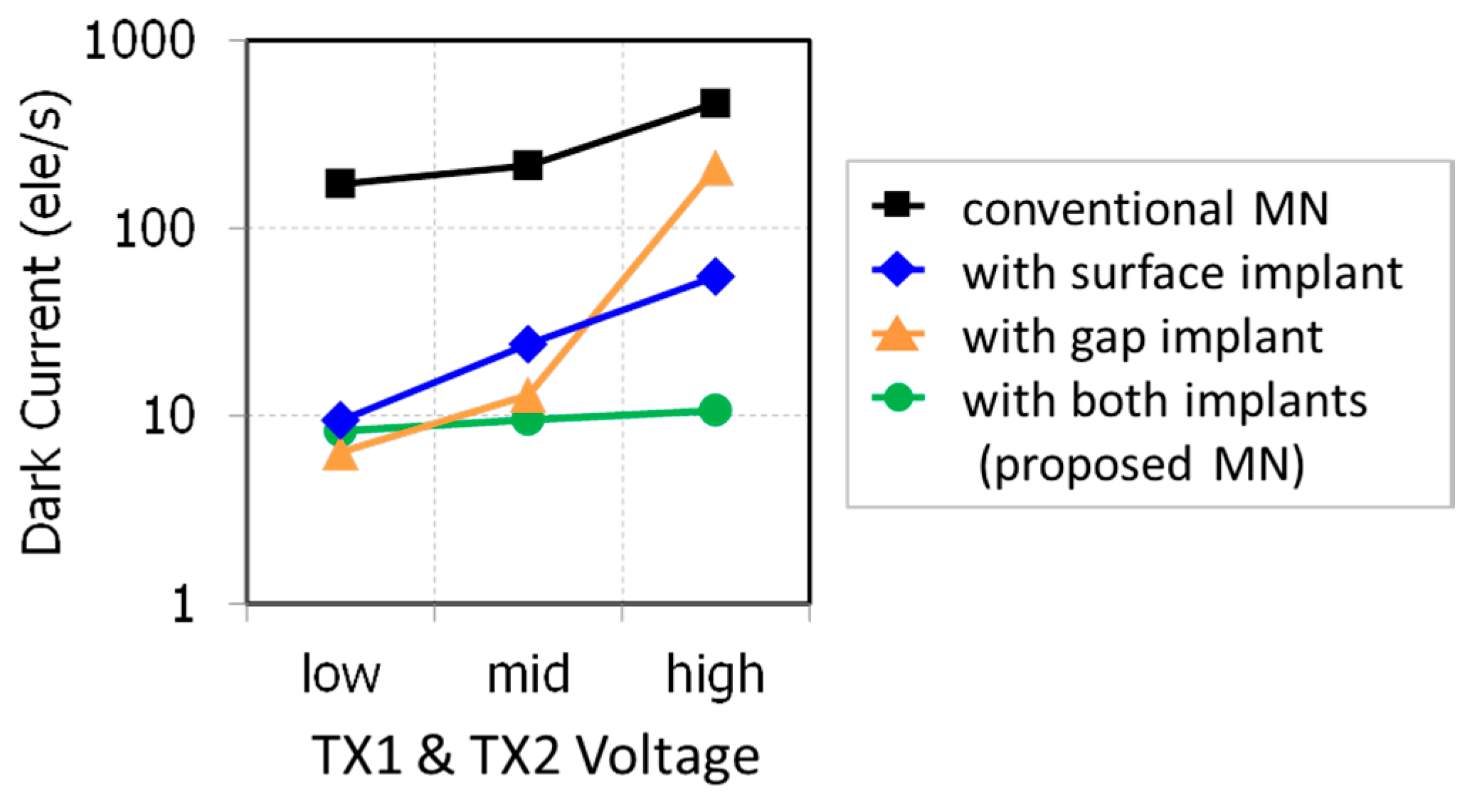
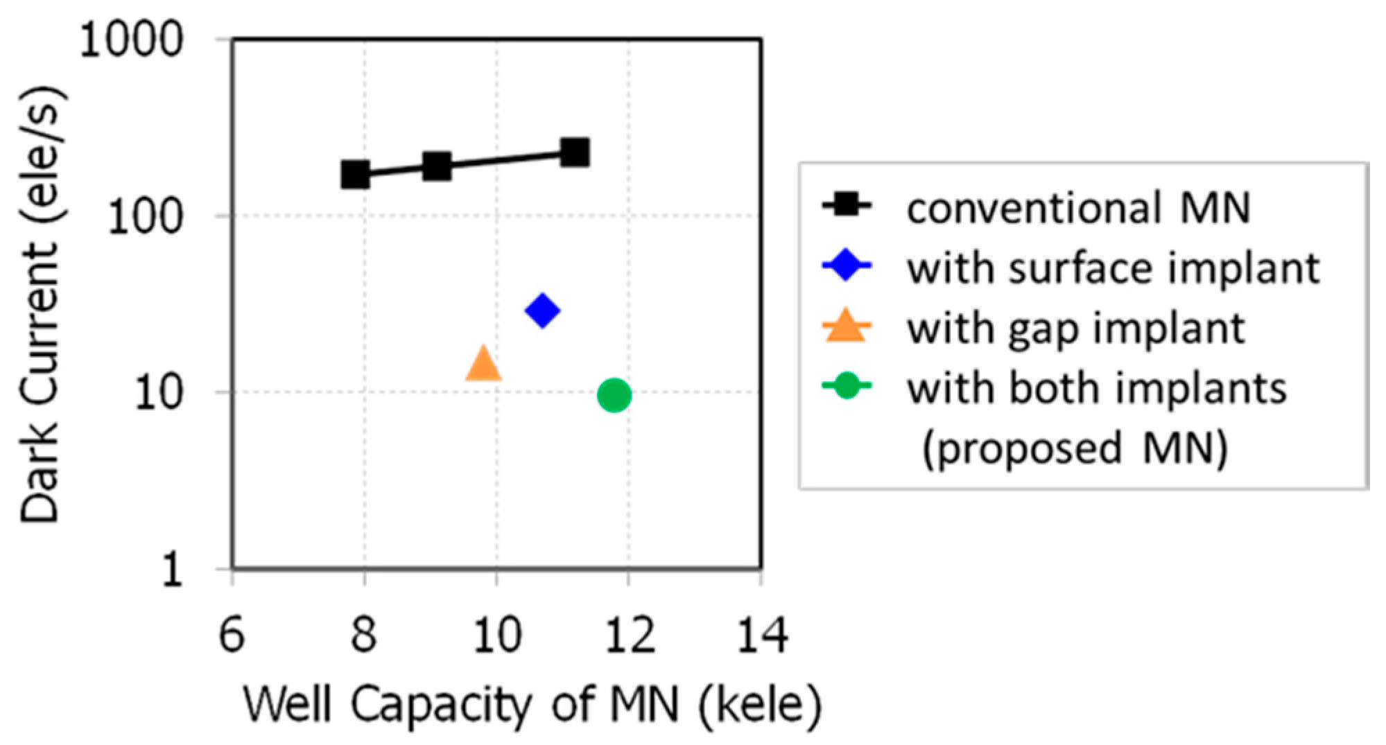
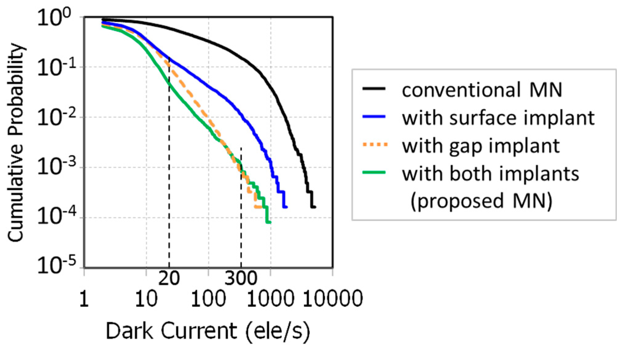
We also proposed and developed new MN structures for low dark current. We verified that high hole concentration under the gap between TX1 and TX2 poly-Si gates was required to suppress MN dark current. Our developed MN structure shows the world smallest dark current of 9.5 e−/s at 60 °C.


