Article

A Quadrature Single Side-Band Mixer with Passive Negative Resistance in Software-Defined Frequency Synthesizer

School of Optical and Electronic Information, Huazhong University of Science and Technology, 1037 Luoyu Road, Wuhan 430074, China
*
Authors to whom correspondence should be addressed.
Sensors 2018, 18(10), 3455; https://doi.org/10.3390/s18103455
Submission received: 6 September 2018 / Revised: 9 October 2018 / Accepted: 9 October 2018 / Published: 14 October 2018
(This article belongs to the Section Sensor Networks)

Abstract

:
Software-defined radio (SDR) is a good solution for complying with the existing and incoming protocols for emerging wireless sensor networks (WSN) and internet of things (IoT) applications. The frequency synthesizer in a SDR tranceiver usually consists of a phase locked loop (PLL) and a post synthesizer. The PLL is the narrow band signal source and the post synthesizer generates wideband outputs by mixing and dividing. Compared with a frequency synthesizer utilizing the wideband PLL, this synthesizer features relatively constant loop parameters and mitigates the requirement for the oscillator. In this paper, a quadrature single side-band (QSSB) mixer with the proposed passive negative resistance (PNR) for frequency mixing in a post synthesizer is presented. The PNR is achieved by biasing the Metal-Oxide-Semiconductor Field-Effect Transistors (MOSFET) of the cross-coupled pair at the deep-triode region periodically and incorporates an inductor and a cap-array as the mixer load. Compared with the traditional single side-band mixers utilizing Inductor-Capacitor (LC) resonant loads or quality factor enhanced (Q-enhanced) LC resonant loads, which suffer from a selectivity versus working range trade-off, the mixer employing the proposed loading structure provides not only a wide operating range, but also a superior image side-band rejection ratio (ISRR). Moreover, the oscillating risk in conventional mixers adopting Q-enhanced LC resonant loads is eliminated. A wideband frequency synthesizer employing the proposed mixer was implemented in a TSMC 0.18 µm CMOS process and the mixer performed ISRR of 40–57 dB and 30–57 dB across 2.5–3 GHz and 2.3–3.2 GHz, respectively. The power consumption of the QSSB mixer, including buffer, is 18 mA from a 1.8 V supply and the active area is 0.445 mm2. The measurement results provide validation that the proposed QSSB mixer is suitable for wideband software-defined frequency synthesizers and other frequency generating systems.

1. Introduction

The wireless sensor network is an enabling technology of the internet of things and has emerged in recent decades. A complete wireless sensor network (WSN) system consists of many randomly deployed sensor nodes, a base station (or sink), a control center and a database, as illustrated in Figure 1. Various types of sensor nodes gather information about physical objects or environmental conditions, including the surrounding temperature, humidity, moisture, water flow and so on. The base station controls these sensor nodes and acts as a gateway to transmit the gathered data back to the control center. Although the use of sensor nodes in a WSN is currently limited to the fixed industrial-scientific-medical (ISM) band, they are perfectly able to conform with the developing trend of the internet of things (IoT) where any sensor node can communicate with the base station employing any wireless protocol. For instance, in a target monitoring field, it would be meaningful if sensor node 1 and sensor node 4 could utilize ZigBee and Bluetooth protocols separately to make contact with the base station, as presented in Figure 1. As WSN and IoT markets are growing rapidly, this multiple-communication-techniques scenario will be ubiquitous in the future.
Until now, many wireless protocols have been used in WSNs and IoT systems including standard mobile telephony (GSM, GPRS), broadband techniques (802.11 a/b/g) and wireless personal area networks (ZigBee, IEEE 802.15.4, Bluetooth,). In addition, many other wireless protocols are springing up, such as the fifth generation (5G), which operates at 3.3–3.6/4.8–5 GHz in China. Some typical protocols with their corresponding main characteristics, covering operating frequencies ranging from 13.56 MHz to 2.4 GHz, are summarized in Table 1. As the bridge connecting the sensor nodes and the control center, the performance of the base station is the bottleneck of the system. To comply with as many protocols as possible, a base station grounded on software-defined radio is a good solution [1], but one which puts stringent requirements on having a frequency synthesizer (FS) with a wider frequency range, and lower phase noise and spurs.
Generally, the FS in software-defined radio (SDR) is composed of a narrow band phase locked loop (PLL) and post synthesis circuit [2,3,4,5,6,7,8,9,10,11,12]. Compared with a wideband PLL employing multiple voltage controlled oscillator (VCO) cores, the PLL in this FS structure characterizes relatively constant loop parameters and releases the requirement for the oscillator. The post synthesis circuit is fed by the PLL outputs and generates wideband outputs by mixing and dividing. For Most transceivers utilize in-phase and quadrature local oscillator (LO) signals to suppress image signals and support advanced quadrature amplitude modulation. A quadrature single side-band (QSSB) mixer is usually adopted in a post synthesis circuit to produce quadrature outputs.
The widely employed QSSB mixers are based on the double-balanced Gilbert structure which features sufficient LO leakage suppression at the output. Moreover, to obtain purity of LO signals, the image side-band signals should also be attenuated. The LC resonant loads are widely utilized in the QSSB mixer to pick out the desired signals [3,6,13,14]. However, the working range and the selectivity conflict with each other. The Q-enhanced LC resonant loads are utilized in the QSSB mixer [5,7,15,16] for better selectivity characteristics, whereas the risk of oscillating is increased. Furthermore, if the mixer starts oscillating, the working range will be limited, because of the injection locked phenomenon, and the phase noise will deteriorate.
In order to release the contradiction between selectivity and working range and reduce the oscillating risk, a QSSB mixer adopting a novel cross-coupled pair is proposed. The cross-coupled pair performs positive resistance characteristics in small output voltage conditions and provides negative resistance in large output conditions. Contrary to the conventional negative-Gm cross-coupled pair in VCO, which performs negative resistance all the time, the proposed structure provides negative resistance under a specified condition, thus reducing the oscillating risk. We name this negative resistance passive negative resistance (PNR). As long as the cross-coupled pair performs the PNR characteristic, the mixer selectivity is swiftly enhanced, because of the positive feedback, and finally reaches a balance due to the negative feedback. Implemented in TSMC 0.18 µm CMOS process, the proposed mixer performs image side-band rejection ratios (ISRR) of 40–57 dB and 30–57 dB across 2.5–3 GHz and 2.3–3.2 GHz respectively, while consuming 18 mA. The measurement results demonstrate the mixer with PNR can provide both wide working range and good selectivity simultaneously. Moreover, the mixer is absolutely stable and the oscillating risk in the conventional mixer employing Q-enhanced resonant loads is eliminated. This QSSB mixer is suitable for wideband software- defined frequency synthesizer and other frequency generating systems.
This paper is organized as follows: The working principle of QSSB mixer is introduced in Section 2 and the proposed QSSB mixer with PNR is provided in Section 3. The measurement results and discussions are presented in Section 4. Finally, conclusions are presented in Section 5.

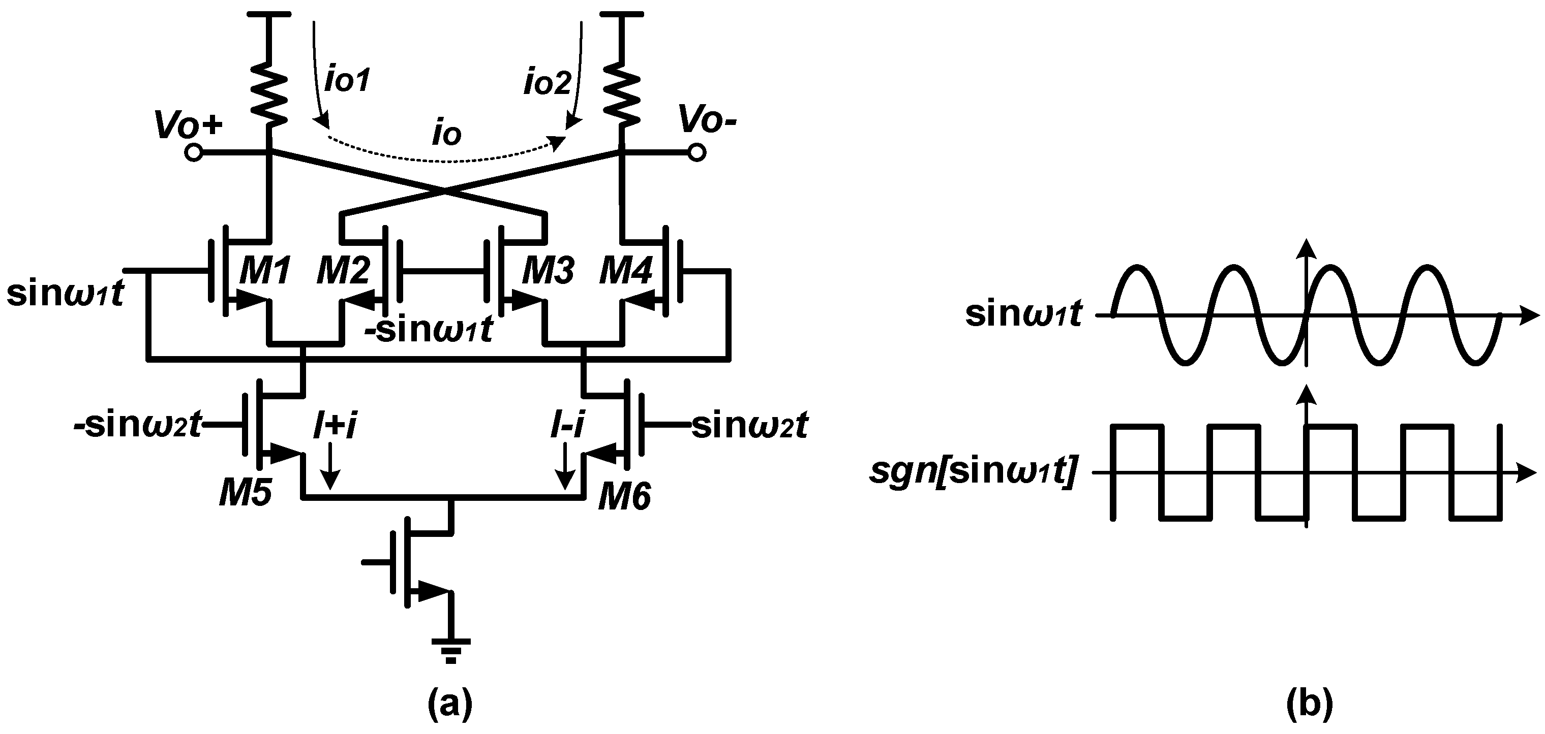
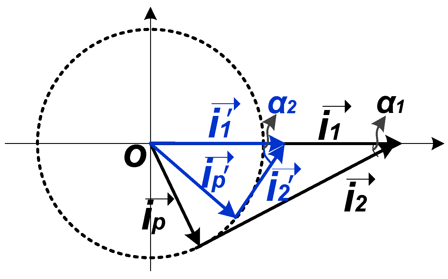
2. Quadrature Single Side-Band Mixer

Mixers can be divided into active mixers and passive mixers. The former feature good isolation and better gain, while the latter are characterized by superior linearity. Because of the unacceptable switch loss and gain attenuation of passive mixers at high frequencies, the mixers utilized in FS are usually based on active mixers. A typical double-balanced active mixer is presented in Figure 2a. The transistors M1M4 work as switches, and M5M6 work as a transconductance pair. If the amplitude of the LO signal is large enough, M1M4 can be regarded as ideal switches. When the LO signal sinω1t is in positive cycle, M1/M4 turn on and M2/M3 turn off, yielding a small-signal differential output current of 2i. Conversely, the output current is −2i when the LO signal is in negative cycle. In other words, the output current direction switches periodically according to the polarity of the LO signal sinω1t. Therefore, the differential output current can be written as
i o = 2 i × s g n [ sin ω 1 t ]  
The characteristics of function s g n [ sin ω 1 t ] are illustrated in Figure 2b. As s g n [ sin ω 1 t ] is an odd function, the Fourier series contains only sinusoid components and is given by
s g n [ sin ω 1 ] = n = 1 b n sin ( n ω 1 t )  
where b n = 2 T ( 0 T 2 sin n ω 1 t d t T 2 T sin n ω 1 t d t ) = 2 ( 1 cos n π ) n π . For the small-signal current 2 i can be written as 2 g m   sin ω 2 t , the output current i o can be represented as
i o = 2 g m n = 1 b n sin ω 2 t × sin n ω 1 t  
It can be observed that the output current contains double side-band components such as ω2ω1, ω2 + ω1 and so on. A single side-band (SSB) mixer is composed of two double-balanced mixers that share the same loads, as presented in Figure 3a. The output current of the left mixer is given in Equation (3) and that of the right mixer is 2 g m n = 1 a n cos ω 2 t cos n ω 1 t ,so the total output current is
i o u t = 2 g m n = 1 k n ( cos ω 2 t × cos n ω 1 t sin ω 2 t × sin n ω 1 t ) = 2 g m n = 1 k n cos ( ω 2 t + n ω 1 t )  
where we assume that the circuit is symmetrical and the Fourier coefficient a n is equal with b n and represented as k n . Therefore, the output current contains only the upper side-band components ω 2 + n ω 1 and the lower side-band signals are suppressed.
A QSSB mixer is made up of two identical SSB mixers with different input signal sequences. If we name the mixer in Figure 3a the I-branch SSB mixer, the Q-branch SSB mixer can be presented in Figure 3b with an output current of
i o u t = 2 g m n = 1 k n ( cos ω 2 t × sin n ω 1 t + sin ω 2 t × cos n ω 1 t ) = 2 g m n = 1 k n sin ( ω 2 t + n ω 1 t )  
By multiplying the output current in Equations (4) and (5) with relative loads, the quadrature signals can be obtained. In reality, the mismatches of the input signals, the circuit asymmetry and the nonlinearity can result in image side-band signals. It is necessary for the loads to have the ability to pick out the desired signals and suppress the image side-band signals.
The LC resonant loads and the Q-enhanced LC resonant loads are widely used in SSB mixers and are presented in Figure 4a,b separately. The cross-coupled negative-Gm pair used in conventional LC VCO is employed for a higher quality factor (Q) and better selectivity. The main drawback of the two kinds of LC loads is the conflict between selectivity and working range, as depicted in Figure 4c. A LC resonant load with higher Q performs better selectivity, while the working range is narrower than those with lower Q. Meanwhile, a mixer utilizing the Q-enhanced LC resonant load has the risk of oscillating, which could reduce the working range and degrade phase noise performance because of the injection locked phenomenon.

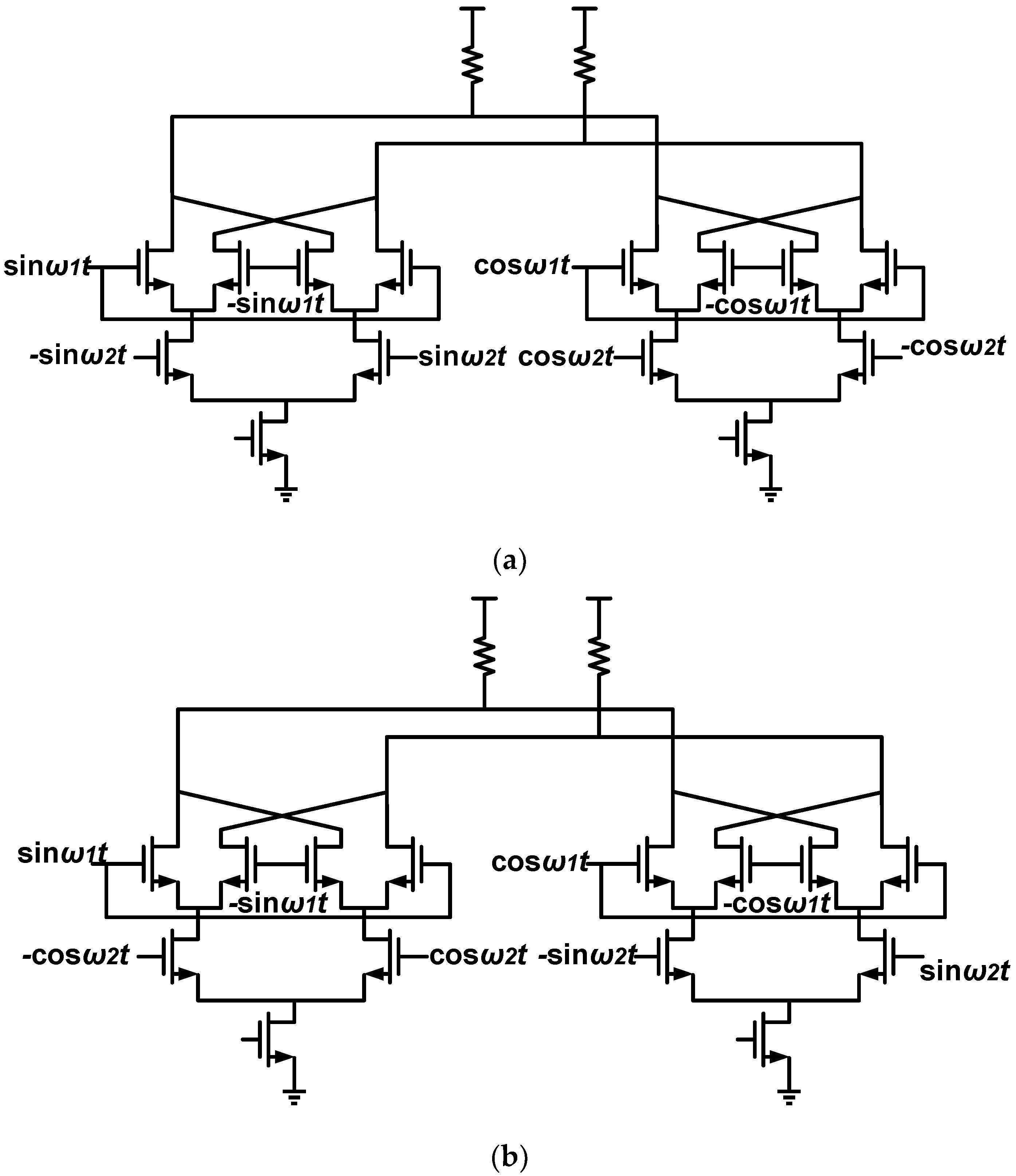
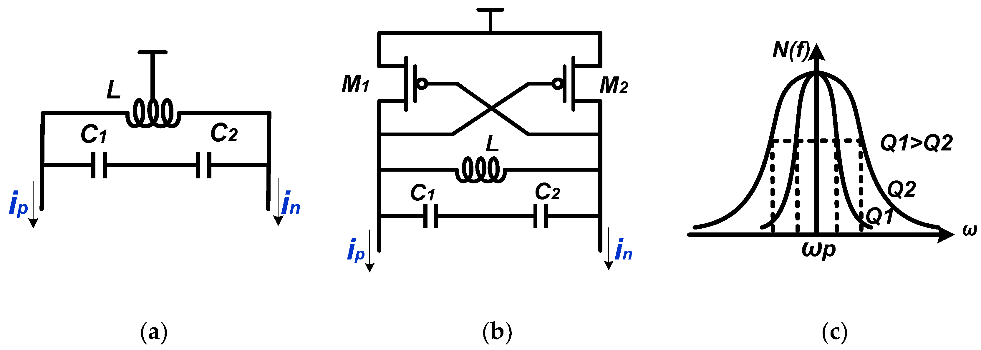
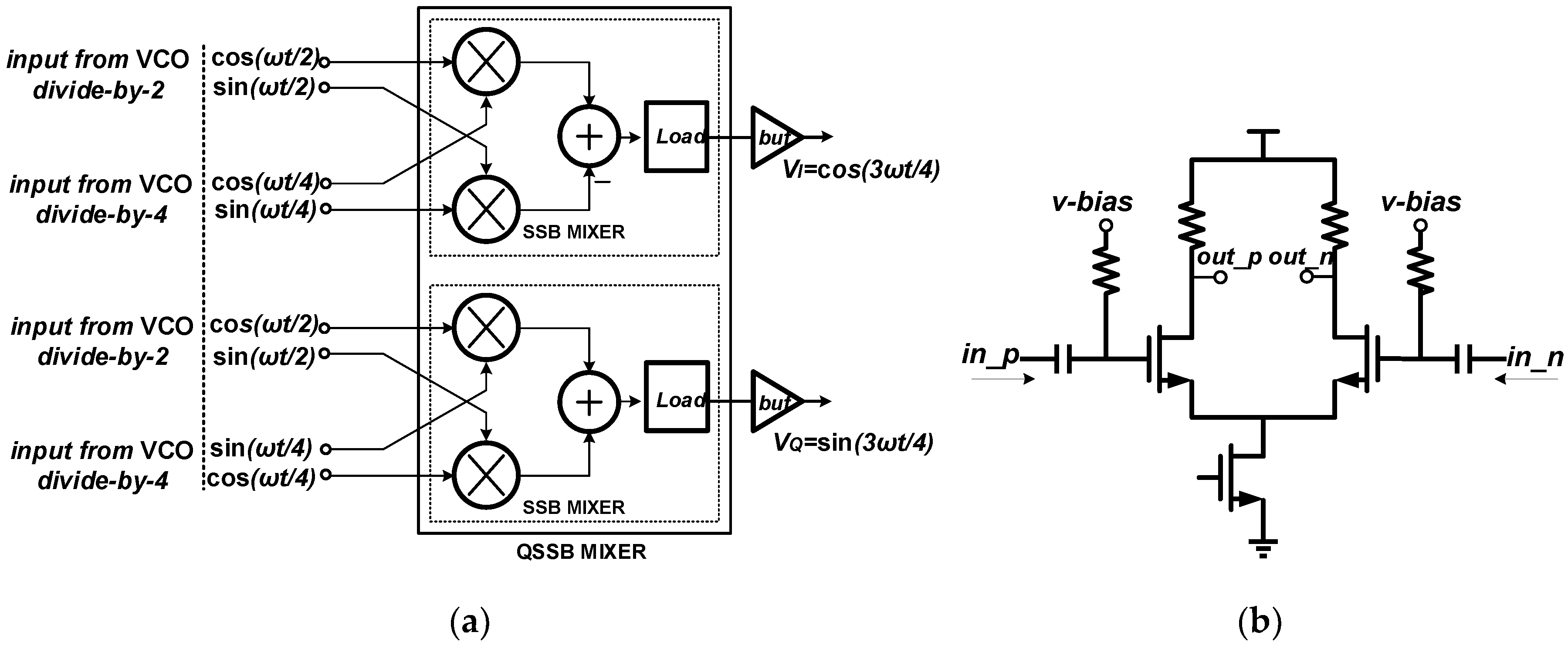
3. Proposed PNR and QSSB Mixer

3.1. The Proposed PNR

In order to release the contradiction between the selectivity and the working range of the conventional LC resonant load, we proposed a novel LC resonant load. The proposed load structure is illustrated in Figure 5a. Given that the circuit is symmetrical, we only analyze the half circuit for simplicity. If the amplitude of the output signal v o u t p is small and the circuit is biased properly, the M3 works at the triode region or the saturate region. As the amplitude increases, or as v s g increases, the M3 could be forced to work at the deep-triode region periodically. In this deep-triode region, with v o u t p decreasing, the v s g and   v a increase accordingly, yielding a decreased source-to-drain voltage v s d . As illustrated in the gray region in Figure 5b, the decreased v s d is accompanied by the decreased i s d . In other words, with v s g increasing, the source-to-drain current i 1 decreases, resulting in a negative resistance. The transient simulation results of v s g , i 1 , and v s g / i 1 are presented in Figure 6, and the negative resistance is depicted in the gray region. This negative resistance is performed only when the output amplitude is large enough and would not be presented if the output amplitude is small. Compared to a mixer utilizing a conventional negative-Gm pair, a mixer adopting the proposed PNR-based load can reduce the risk of oscillation.
As long as the PNR is performed, the quality factor of the proposed load structure increases, resulting in a larger output impedance. For a mixer that is biased with a current source, the current i p in Figure 5a is usually fixed, and the amplitudes of v o u t p and v o u t n would increase as impedance increases, which in turn compels M3/M4 to work in the deep-triode region for a long time and produces larger than average PNR. This is a positive feedback that makes the output amplitude become larger and larger. Because M3 works in the deep-triode region for a long time and the average value of i 1 keeps decreasing, the amplitude of i 2 has to be decreased to maintain the vector relationship between i p , i 1 and i 2 , as illustrated in Figure 7. When PNR is not performed and i 1 is relatively large, the current i 2 is also large. Once PNR is performed, accompanied by a decreased average current i 1 , the current vector across the LC tank switches from i 2 to i 2 with a smaller amplitude. This is a negative feedback that maintains the balance of the output amplitude. In conclusion, the positive feedback produces large negative resistance and ensures high Q for superior selectivity, while the negative feedback guarantees the balance of the circuit.

3.2. The Proposed QSSB Mixer

The proposed QSSB mixer in a wideband FS is presented in Figure 8. The FS is composed of a PLL and post synthesis circuit. The PLL is made up of a phase frequency detector (PFD), a charge pump (CP), an off-chip loop filter, an integrated VCO and a programmable multi-modulus divider (PMMD) and provides the differential outputs ranging from 3.2 to 4.8 GHz. The post synthesis circuit consists of the divide-by-2 dividers, the QSSB mixer, and the quadrature divider (QIDIV) and is fed by the differential VCO outputs. The first divide-by-2 divider is based on the conventional current-mode logic (CML) structure and gives the 1.6–2.4 GHz quadrature outputs, while the second one is a regenerative divider and realizes the function of the quadrature-in quadrature-out (QIQO). The outputs of the two dividers are delivered to the QSSB mixer to produce the 2.4–3.6 GHz quadrature outputs. By combining the two quadrature signal sources, the 1.6–3.6 GHz quadrature outputs are obtained. By sending the quadrature outputs into the QIDIV, that consists of 6 stages of divide-by-2 dividers, the output frequencies ranging from 30 M to 3.6 GHz are covered. Compared with a PLL utilizing multiple VCO cores and a set of dividers to produce the wideband outputs, the PLL in the proposed FS adopts only one VCO core with differential outputs covering 3.2–4.8 GHz, which reduces the loop parameters variation and is beneficial for optimization. Moreover, the PMMD in the PLL could work at a lower frequency and consume less power.
The QSSB mixer is composed of two identical SSB mixers and two output buffers. A 3-bit cap array is utilized to extend the operating range. Meanwhile, the source degeneration technique in LO ports is employed to further improve the linearity, splitting the RF ports into 8 devices. The QSSB mixer structure is presented in Figure 9a, with two input frequencies at ω / 2 and ω / 4 and an ideal output frequency at 3 ω / 4 , where ω represents the VCO oscillating frequency. To avoid loading effects and provide better drive capability, output buffers are employed and the structure is presented in Figure 9b.
The transient output waves, the operating range and the ISRR of a QSSB mixer employing the conventional LC resonant load, the Q-enhanced LC resonant load, and the proposed load are simulated separately for comparison. The Q-enhanced LC resonant load is similar to the proposed one in Figure 5 except M3/M4, and the conventional LC resonant load excludes M1M4. When biased with the fixed current source, the power consumptions of the mixers adopting different loads are the same. The simulation is based on the post synthesizer, fed by the ideal differential VCO outputs.
The transient simulation results of the mixer with fixed cap array control signals and different types of loads are presented in Figure 10a–c. The input frequency is set to be 4.4 GHz and the ideal output frequency is 3.3 GHz. The peak-to-peak voltage of the mixer outputs reach 1.8 V when the mixer adopts the Q-enhanced LC resonant loads, as presented in Figure 10a. After passing through the following buffer, the output amplitude does not appear to change. In fact, the mixer is injection locked under this condition. When employing the conventional LC resonant load, the mixer produces unclean signals because of the limited selectivity, and the transient outputs are presented in Figure 10b. The pure output signals are provided at the mixer output with an amplitude of about 0.5 V when utilizing the proposed load, as depicted in Figure 10c.
The ISRR versus the operating range at the mixer’s outputs and the buffer’s outputs are presented in Figure 11a,b respectively. For the two inputs ω / 2 and ω / 4 ,and the desired output locates at 3 ω / 4 , the image side-band is ω / 4 , the same as one of the inputs. Thus, the input signals could degrade the ISRR directly by feedthrough or other side-effects. When employing the Q-enhanced LC resonant load, the mixer provides the best ISRR performance at the mixer’s outputs with the maximum value of about 50 dB at 3.375 GHz. However, the output frequency range is 3.15 G–3.6 GHz because of the injection locked phenomenon. The mixers adopting the LC resonant load and the proposed load perform over a wider operating range, and the ISRR performance of the former is superior for the absent utilization of nonlinearity components in the LC load. In reality, at the outputs of the mixer employing the LC resonant load, apart from the image side-band signal, some other side-band signals also exist because of the low Q LC tank, leading to the unclear transient outputs as presented in Figure 10b. The ISRR simulation results at the mixer’s outputs are presented in Figure 11a. At the buffer’s outputs, the ISRR of the mixer utilizing the LC or Q-enhanced LC resonant load deteriorates and that of the mixer adopting the proposed load improves from 3.2 G–3.6 GHz; the simulation results are depicted in Figure 11b. Compared with the mixer employing the conventional loads, the proposed one, adopting the PNR-based load, performs over a wider operating range and has a higher ISRR simultaneously.
There are two reasons why the ISRR changes at the buffer output. The first one is the different conversion gains at different side-bands. The signal power at the image side-band is smaller than that at the desired side-band, and the latter would saturate the output buffer, resulting in a small gain. For example, the mixer’s output amplitude reaches 0.9 V as presented in Figure 10a. After being amplified by the buffer, the amplitude is still about 0.9 V, indicating that the desired signal is amplified to a limited extent, whereas the signals at the image side-band would be amplified, thus degrading the ISRR at the buffer’s output. The second one is the nonlinearity effects. The buffer would work in the nonlinear region if the input signal is large, producing many harmonic tones. These tones could locate at the same frequency with different phase and amplitude and could be superimposed or cancel each other out. For instance, if the tone at the image side-band is enhanced while that at the desired side-band is suppressed, the ISRR deteriorates. This is what happens to the mixer that enriches harmonic tones at the mixer core outputs. As for the mixer adopting the proposed load, the desired side-band would be amplified properly because of fewer harmonic productions at the mixer outputs.
The overall ISRR simulation results at the mixer’s outputs and the buffer’s outputs by tuning the mixer cap-array are presented separately in Figure 12a,b. The output frequency range covers 2.25–4.5 GHz. At the mixer core outputs, the ISRR is 33–39.5 dB, and is 30–42 dB at the buffer outputs. In 2.4–3.6 GHz, the ISRR are 35.8–37.3 dB and 35.2–41.8 dB at the mixer core outputs and the buffer outputs, respectively.

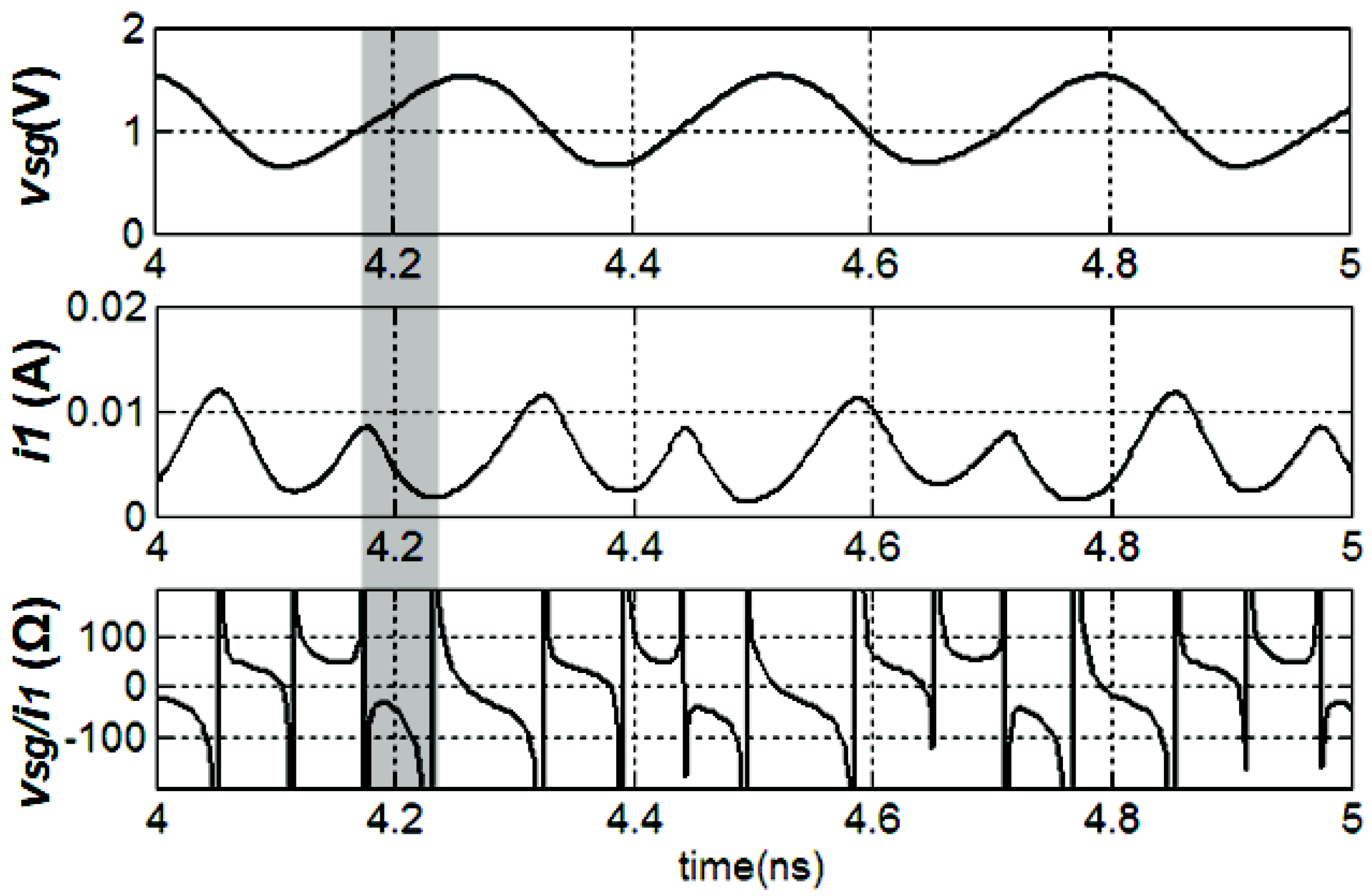
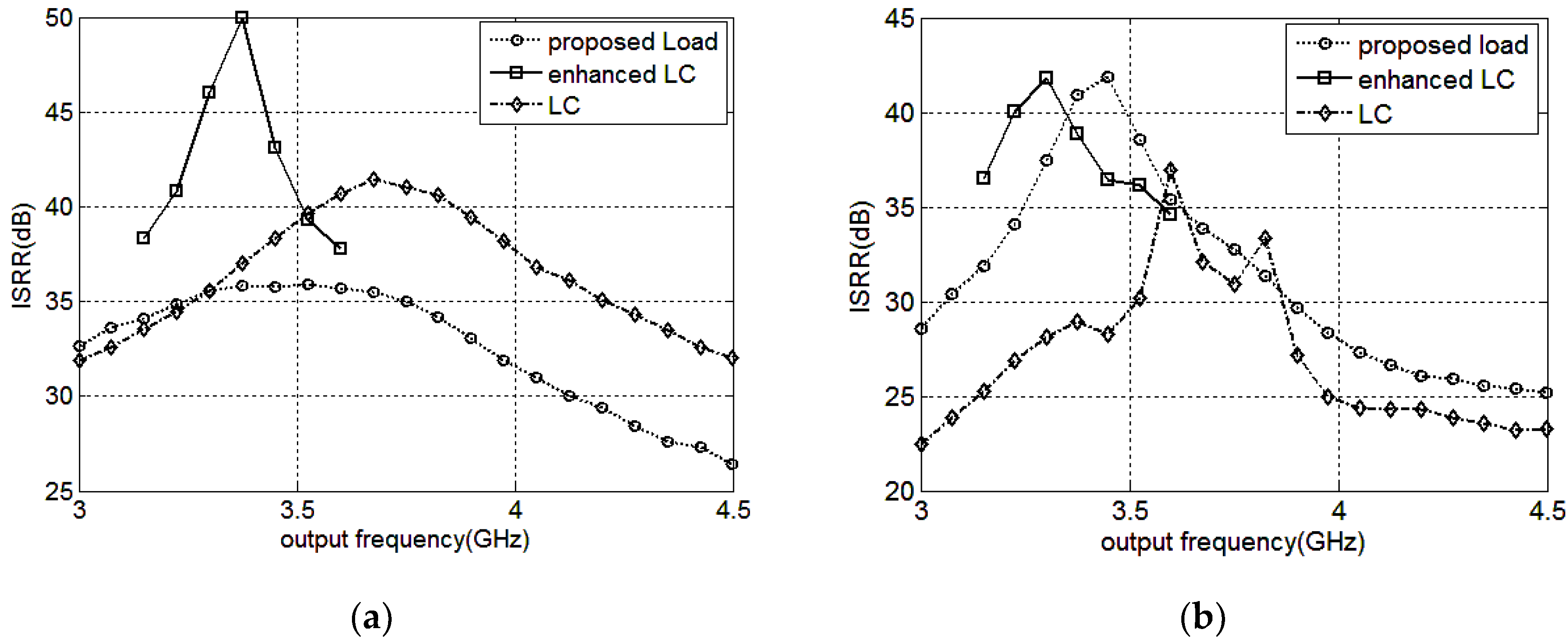
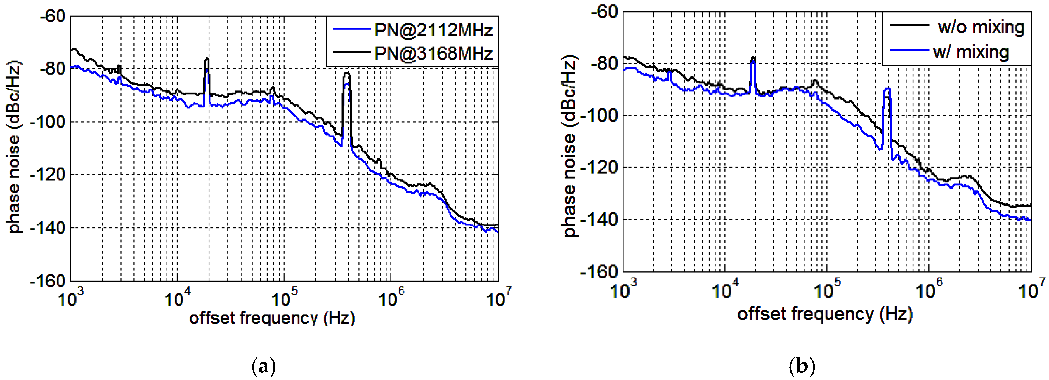
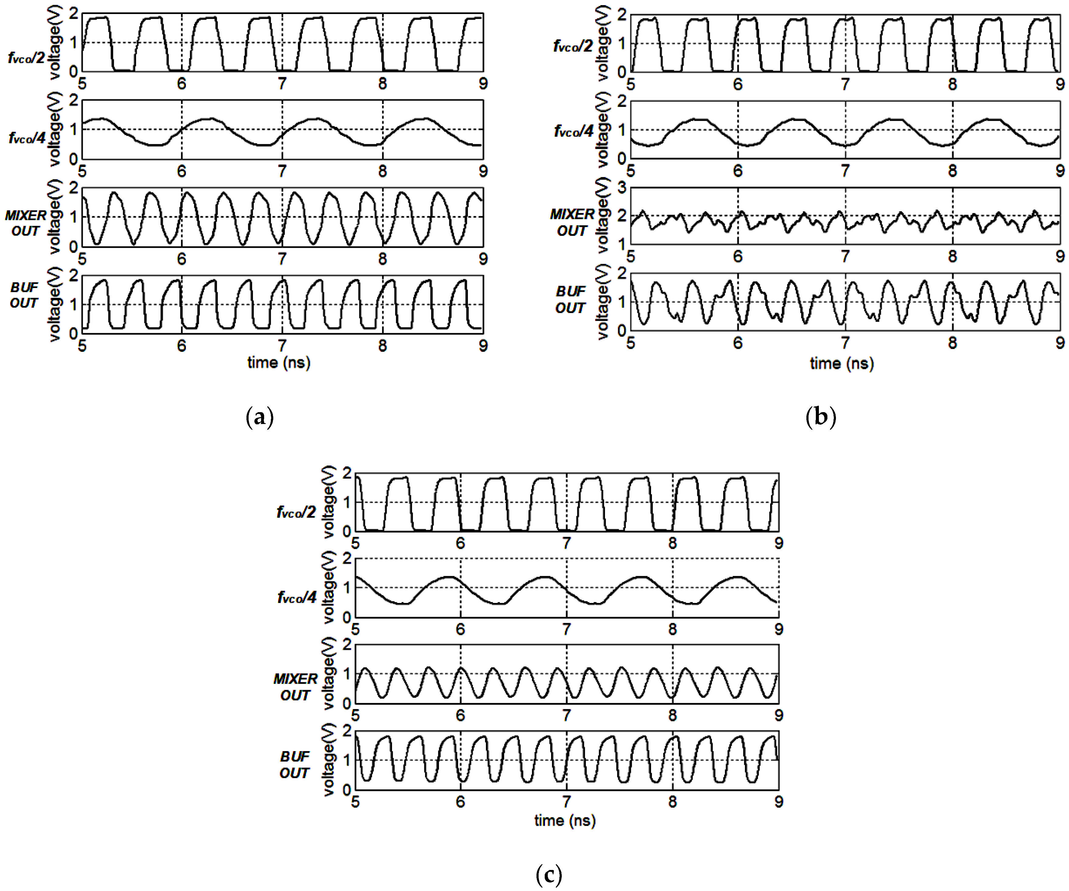
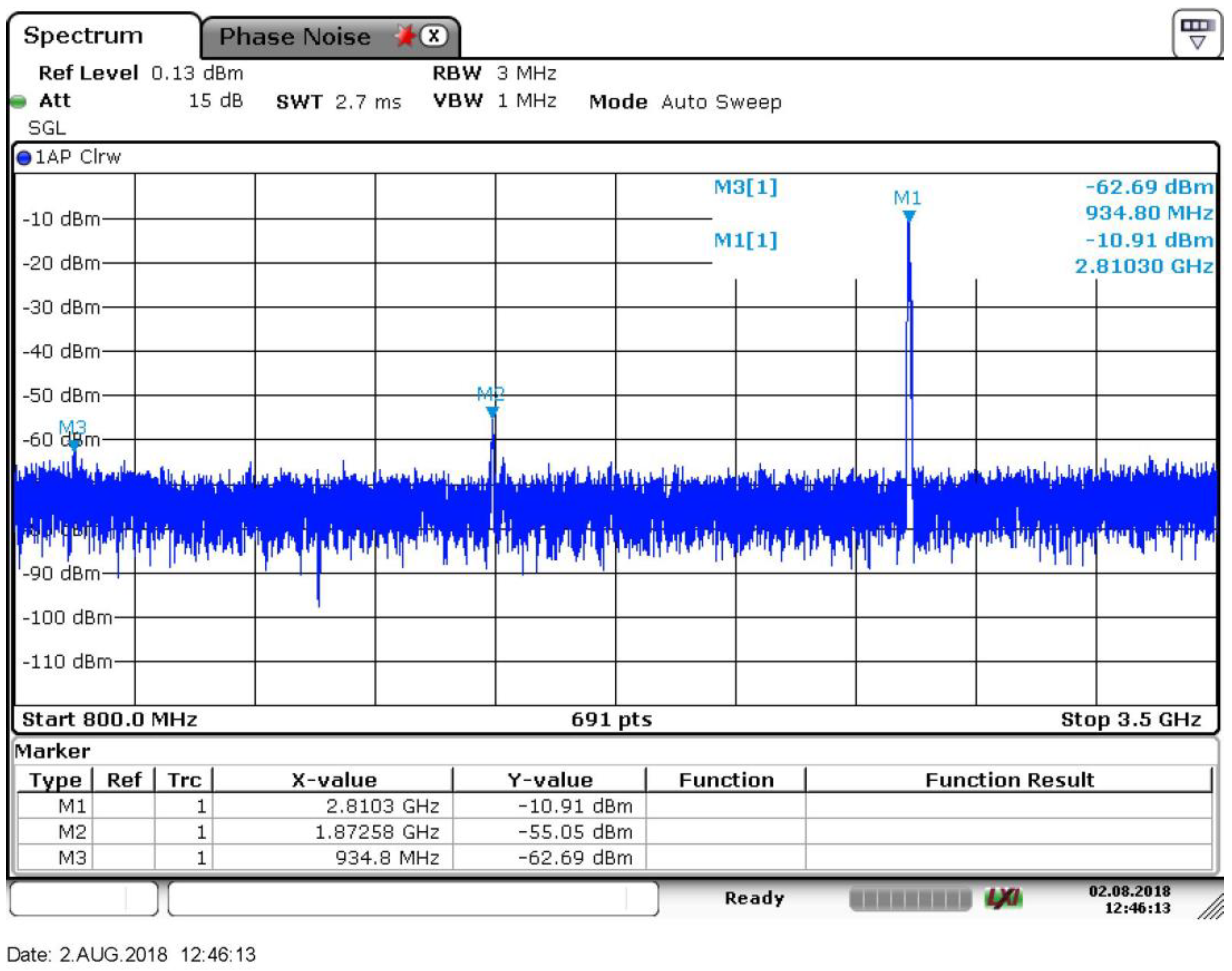
4. Measurement Results and Discussion

The proposed QSSB mixer and the frequency synthesizer are implemented in a TSMC 180 nm CMOS RF process, and the micrograph of the post synthesis circuit is presented in Figure 13 with an area of 1.25 mm2. This process provides one poly layer and six metal layers, with a 4.6   μ m ultra-thick top metal (M6) and 8.15 μ m distance between M6 and the substrate. The permittivity, thickness and resistivity of the substrate are 11.9, 250   μ m and 10 Ω cm, separately. Because of the adopted LC tank in the mixer core, most of the area is made up of the inductors and the total active area of the QSSB mixer is about 0.445 mm². The layout of the QSSB mixer is designed as symmetrically as possible for better side-band rejection. The output spectrum and phase noise are measured by Rohde Schwarz FSV7 signal analyzer. The ISRR is measured through the output spectrum by calculating the power level discrepancy between the desired signal and the image side-band signal. In this condition, the FS is unnecessarily locked, and the output frequency is switched by controlling the VCO cap array. By changing the QSSB mixer cap array, the eight frequency-ISRR curves are obtained. The phase noise is measured using the signal analyzer directly in the locked state.
The output spectrum is presented in Figure 14. The two input signals are at 1872 MHz and 936 MHz with the power level of −55 dBm and −62.7 dBm, respectively. The desired tone is at 2808 MHz and the signal power is about −10.9 dBm, producing an ISRR of 51.8 dB. The total ISRR measurement results against the output frequency and the ISRR simulation results, with 500 fF parasitic capacitance, are presented in Figure 15a. It can be observed that the measured operating frequencies are smaller than those of the simulation results presented in Figure 12b, mainly due to the parasitic capacitors decreasing the LC resonating frequencies. When including the 500 fF parasitic capacitors, the resonating frequency simulation results are in accordance with the measurement results. The simulated and measurement resonant frequencies versus the mixer cap-array control signals are presented in Figure 15b. When the parasitic capacitance is set at 500 fF, the simulation results are consistent with the measurement results as shown in Figure 15a. The peak ISRR measurement result is about 57 dB and is larger than that of the simulation result. Furthermore, the measurement operating bandwidth of each curve is much smaller than the simulation result. Considering the conflict between Q and bandwidth, the measurement results imply that the measured quality factor of the implemented load is much higher than the simulation result. The ISRR performances are 40–57 dB and 30–57 dB across 2.5–3 GHz and 2.3–3.2 GHz, respectively. From 3–3.6 GHz, the ISRR drops off drastically, partially because the inverter buffer attenuates the high frequency signals. The inverter buffer delivers −5~0 dBm output power at 30 M–3 GHz while providing −5~−15 dBm at 3–3.6 GHz, implying the buffer attenuates 5–10 dB at 3–3.6 GHz. If the outputs locate at 3–3.6 GHz, the image side-band signals locate at 1–1.2 GHz. In this condition, the desired outputs are attenuated while the image side-band signals are not suppressed to the same extent, leading to the drop-off in the ISRR characteristic. In addition, the gain mismatch and phase imbalance of the VCO outputs can also degrade the ISRR performance. By optimizing the inverter buffer and compensating the gain and phase mismatch of the VCO outputs, the ISRR performance could be improved.
The phase noise measurement results at 2112 MHz and 3168 MHz are presented in Figure 16a, and the spot phase noise at 10 KHz and 1 MHz offsets are −92, −88 and −123, −120 dBc/Hz, respectively. The phase noise distinctions between 2112 MHz and 3168 MHz from 1 KHz to 10 MHz offsets are 3–4 dB. The output frequency 3168 MHz is produced by mixing 2112 MHz and its divide-by-2 output 1056 MHz. Therefore, the two signals originate from the same core synthesizer signal and the phase noise deviation is mainly caused by the QSSB mixer. Ideally, as frequency multiplied by a factor of 1.5, the phase noise would increase about 20 log 1.5 3.5 dB, which is in accordance with the measurement results, indicating the noise contributed by the mixer is negligible. The spurs at 20 KHz and 400 KHz are caused by the interfering signals at the input. By employing a pure reference signal, these spurs can be eliminated. The desired VCO tuning range is 3.2–4.8 GHz. In fact, the measurement tuning range of the VCO is 2.5–5 GHz for an efficient frequency margin. Therefore, the target output frequency can be produced by mixing indirectly or by PLL directly. The phase noise measurement results at 2376 MHz, with or without the mixing process, are illustrated in Figure 16b. When directly output, the VCO oscillates at 4752 MHz and the target frequency is obtained by divide-by-2 operation. Otherwise, the VCO works at 3168 MHz and the desired frequency is generated by mixing. As can be seen, the phase noise of the outputs given indirectly is superior to that given directly. In fact, the phase noise of the core synthesizer signal at 3168 MHz is superior to that at 4752 MHz for the lower operating frequency. Although the mixer induces some noise, the output signal originating from 3168 MHz is purer than that from 4752 MHz. The QSSB mixer provides another option for low phase noise frequency synthesizer design.
The overall phase noise performances from 1.6 GHz to 2.4 GHz and 2.4 GHz to 3.6 GHz are summarized in Figure 17. The 2.4–3.6 GHz output frequencies are the mixing products of 1.6–2.4 GHz. The spot phase noise at 10 KHz and 1 MHz offsets are less than −87 dBc/Hz and −118 dBc/Hz respectively. Around 2.4 GHz, it can be observed that the phase noise of the outputs without mixing are inferior to those with mixing. This is in accordance with the former discussion. With output frequency decreasing, the phase noise decreases accordingly and the noise of the outputs without mixing are superior to those with mixing for the lower carry frequencies. The performance comparison between this work and the references is presented in Table 2. The frequency synthesizers adopting SSB mixers are mostly for Ultra Wide Band (UWB) application and care about the ISRR at discrete frequencies, such as in References [8,9,17,18,19,20,21,22,23,24], so performance can be optimized by tuning the capacitor array. The ISRR of the SSB mixer in Reference [6] is about 42 dB in the continuous range of 5–6 GHz by utilizing harmonic rejection technique. If employing this technique, the signals v(t), v(t + T/4) and v(t − T/4) are required to cancel the third- and the fifth-order harmonics and obtain a better ISRR. However, the output frequencies are 5 / 4 times larger than the input frequencies, which is not adequate for some applications. For the proposed PNR which can improve the selectivity of the LC resonant loads, the mixer employing the PNR-based load performs better ISRR than the mixer adopting the LC loads. The oscillating risk of the conventional mixer utilizing the Q-enhanced LC resonant loads is also eliminated. Compared to these earlier works, the proposed QSSB mixer can provide superior ISRR in a wideband continuous output frequency range. However, the proposed load presents a PNR characteristic when the output amplitude is large enough, implying that the mixer consumes a lot of power. By optimizing the bias point of the PNR, power consumption would be improved. This QSSB mixer is suitable for a wideband frequency synthesizer and frequency generating system such as that in the SDR based WSN base station.

5. Conclusions

The working bandwidth and selectivity conflict with each other in traditional mixers employing LC- or Q-enhanced LC-resonant loads. In order to release this contradiction, a QSSB mixer with the proposed PNR-based load for a wide operating range and high ISRR is presented in this paper. By biasing the MOSFETs at the deep linear region periodically, the PNR is obtained to enhance the parallel LC resonator quality factor. A QSSB mixer with the PNR-based load was implemented in a TSMC 180 nm CMOS process and performed ISRR of 40–57 dB and 30–57 dB across 2.5–3 GHz and 2.3–3.2 GHz, respectively. Moreover, the noise induced by the mixer was negligible. The measurement results demonstrate that the proposed QSSB mixer not only works in a wide frequency range but also performs high ISRR. This QSSB mixer is suitable for a wideband frequency synthesizer and frequency generating system such as that in the SDR based WSN base-station.

Author Contributions

A.H. conceived the idea; D.L. and A.H. implemented the chip and wrote the paper; K.Z. revised the manuscript.

Funding

This work was supported by the National Natural Science Foundation of China (No. 61874163), the National Science and Technology Major Project (No.2017ZX01032-101), the Introduced Innovative R&D Team of Dongguan (No.201760712600139), and the Fundamental Research Funds for the Central Universities (HUST:2018KFYYXJJ056).

Conflicts of Interest

The authors declare no conflict of interest.

References

  1. Giannini, V.; Nuzzo, P.; Soens, C.; Vengattaramane, K.; Ryckaert, J.; Goffioul, M.; Debaillie, B.; Borremans, J.; Van Driessche, J.; Craninckx, J.; et al. A 2-mm2 0.1–5 GHz Software-Defined Radio Receiver in 45-nm Digital CMOS. IEEE J. Solid-State Circuits 2009, 44, 3486–3498. [Google Scholar] [CrossRef]
  2. Deng, W.; Hara, S.; Musa, A.; Okada, K.; Matsuzawa, A. A Compact and Low-Power Fractionally Injection-Locked Quadrature Frequency Synthesizer Using a Self-Synchronized Gating Injection Technique for Software-De fined Radios. IEEE J. Solid-State Circuits 2014, 49, 1984–1994. [Google Scholar] [CrossRef]
  3. Yu, S.; Baeyens, Y.; Weiner, J.; Koc, U.; Rambaud, M.; Liao, F.; Chen, Y.; Kinget, P.R. A Single-Chip 125-MHz to 32-GHz Signal Source in 0.18-um SiGeBi CMOS. IEEE J. Solid-State Circuits 2011, 46, 598–614. [Google Scholar] [CrossRef]
  4. Osmany, S.A.; Herzel, F.; Scheytt, J.C. An Integrated 0.6–4.6 GHz, 5–7 GHz, 10–14 GHz and 20–28 GHz Frequency Synthesizer for Software-Defined Radio Applications. IEEE J. Solid-State Circuits 2010, 45, 1657–1688. [Google Scholar] [CrossRef]
  5. Rong, S.; Yin, J.; Luong, H.C. A 0.05- to 10-GHz, 19- to 22-GHz, and 38- to 44-GHz Frequency Synthesizer for Software-Defined Radios in 0.13-μm CMOS Process. IEEE Trans. Circuits Syst. II 2016, 63, 109–113. [Google Scholar] [CrossRef]
  6. Zhou, J.; Li, W.; Huang, D.; Lian, C.; Li, N.; Ren, J.; Chen, J. A 0.4–6-GHz Frequency Synthesizer Using Dual-Mode VCO for Software-Defined Radio. IEEE Trans. Microw. Theory Technol. 2013, 61, 848–859. [Google Scholar] [CrossRef]
  7. Lu, T.; Chen, W. A 3–10 GHz, 14 Bands CMOS Frequency Synthesizer with Spurs Reduction for MB-OFDM UWB System. IEEE Trans. Very Large Scale Integr. (VLSI) Syst. 2012, 20, 948–958. [Google Scholar] [CrossRef]
  8. Lee, J. A 3-to-8-GHz Fast-Hopping Frequency Synthesizer in 0.18-um CMOS Technology. IEEE J. Solid-State Circuits 2006, 41, 566–573. [Google Scholar] [CrossRef]
  9. Liang, C.; Liu, S.; Chen, Y.; Yang, T.; Ma, G. A 14-band Frequency Synthesizer for MB-OFDM UWB Application. In Proceedings of the IEEE International Solid-State Circuits Conference (ISSCC), San Francisco, CA, USA, 6–9 February 2006; pp. 428–437. [Google Scholar]
  10. Kim, N.-S.; Rabaey, J.M. A 3.1–10.6-GHz 57-Bands CMOS Frequency Synthesizer for UWB-Based Cognitive Radios. IEEE Trans. Microw. Theory Tech. 2018, 66, 4134–4146. [Google Scholar] [CrossRef]
  11. Shanthi, T.; Krishnamurthi, V. FPGA Based Frequency Synthesizer for 14-Band MB-OFDM UWB Transceivers. In Proceedings of the International Conference on Emerging Trends in Engineering, Technology and Science (ICETETS), Pudukkottai, India, 24–26 February 2016; pp. 1–4. [Google Scholar]
  12. Ismaili, Z.; Ajib, W.; Gagnon, F.; Nabki, F. A 0.13 μm CMOS Fully Integrated 0.1∼12 GHz Frequency Synthesizer for Avionic SDR Applications. In Proceedings of the IEEE International Symposium on Circuits and Systems (ISCAS), Baltimore, MD, USA, 28–31 May 2017; pp. 1–4. [Google Scholar]
  13. Ko, J.; Gharpurey, R. A Pulsed UWB Transceiver in 65 nm CMOS with Four-Element Beam forming f or 1 Gbps Meter-Range WPAN Applications. IEEE J. Solid-State Circuits 2016, 51, 1177–1187. [Google Scholar] [CrossRef]
  14. Peng, Y.; Zhang, L.; Fu, J.; Wang, Y. Analysis and Design of a Broadband SiGe HBT Image-Reject Mixer Integrating Quadrature Signal Generator. IEEE Trans. Microw. Theory Tech. 2016, 64, 688–698. [Google Scholar] [CrossRef]
  15. Lee, S.; Lai, C.; Chiou, H. A Filter-based, SSB Mixer for UWB Application. In Proceedings of the IEEE International Workshop on Radio-Frequency Integration Technology (RFIT), Singapore, 30 November–2 December 2005; pp. 109–112. [Google Scholar]
  16. Li, W.; Cheng, K.M. A CMOS Transformer-Based Current Reused SSBM and QVCO for UWB Application. IEEE Trans. Microw. Theory Tech. 2013, 61, 2395–2401. [Google Scholar] [CrossRef]
  17. Li, W.; Cheng, K.K.M. A Single-PLL UWB Frequency Synthesizer Using Current Reusing SSB Mixer. In Proceedings of the IEEE International Conference of Electron Devices and Solid-State Circuits (EDSSC), Hong Kong, China, 16 August 2010; pp. 1–4. [Google Scholar]
  18. Wang, C.; Li, W.; Wang, C.K.; Shih, H.; Yang, T. A 3–10 GHz Full-Band Single VCO Agile Switching Frequency Generator for MB-OFDM UWB. In Proceedings of the IEEE Asian Solid-State Circuits Conference (ASSCC), Jeju, Korea, 12–14 November 2007; pp. 75–78. [Google Scholar]
  19. Kim, J.; Jung, S.; Jung, J.; Sung, S.-K.; Lee, K.Y.; Nam, C.; Park, B.-H.; Choi, S. A Design of the Frequency Synthesizer for UWB Application in 0.13 μm RF CMOS process. In Proceedings of the IEEE International Workshop on Radio-Frequency Integration Technology (RFIT), Singapore, 9–11 December 2007; pp. 318–321. [Google Scholar]
  20. Zheng, H.; Luong, H.C. A 1.5 V 3.1 GHz–8 GHz CMOS Synthesizer for 9-Band MB-OFDM UWB Transceivers. IEEE J. Solid-State Circuits 2007, 42, 1250–1260. [Google Scholar] [CrossRef]
  21. Kuo, Y.F.; Weng, R.M. Regenerative frequency divider for 14 sub-band UWB applications. Electron. Lett. 2008, 44, 111–112. [Google Scholar] [CrossRef]
  22. Yang, Y.; Weng, S.L. 9.8 mW CMOS frequency synthesizer for mode-I UWB transceivers. Electron. Lett. 2010, 46, 179–180. [Google Scholar] [CrossRef]
  23. Lo, Y.; Kiang, J. A Single-Sideband Mixer with Band Selection through an Output Switching Quad. In Proceedings of the European Microwave Conference (EuMC), Paris, France, 28–30 September 2010; pp. 1130–1133. [Google Scholar]
  24. Wang, M.; Saavedra, C.E. Fully Monolithic Single-Sideband Upconverter Mixer with Sideband Selection. In Proceedings of the IEEE MTT-S International Microwave Symposium, Baltimore, MD, USA, 5–10 June 2011; pp. 1–4. [Google Scholar]
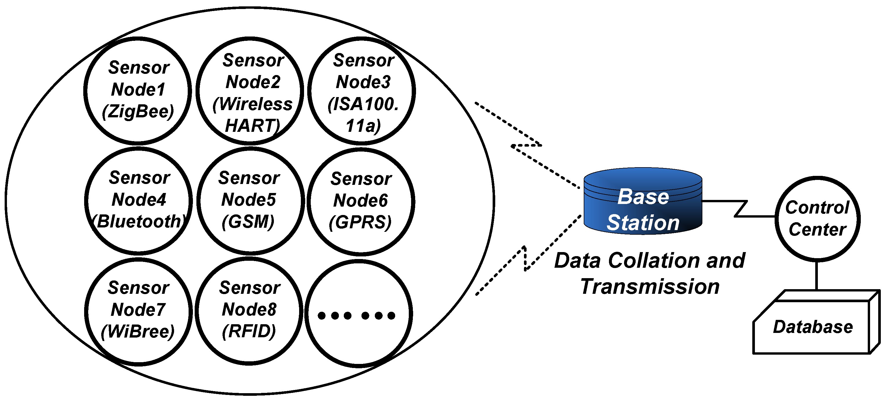
Figure 1. A typical wireless sensor network (WSN) topology.
Sensors 18 03455 g001
Figure 2. (a) Typical double-balanced active mixer; (b) characteristics of the switching signal.
Sensors 18 03455 g002
Figure 3. (a) The I-branch single side-band mixer; (b) the Q-branch single side-band mixer.
Sensors 18 03455 g003
Figure 4. (a) The LC resonant load; (b) The Q-enhanced LC resonant load; (c) The tuning curve of the LC resonator.
Sensors 18 03455 g004
Figure 5. (a) The proposed LC resonant loads with passive negative resistance (PNR); (b) The I-V curve of M3/M4.
Sensors 18 03455 g005
Figure 6. The transient simulation results of v s g , i 1 and output resistance.
Sensors 18 03455 g006
Figure 7. The vector interpretation of current changing.
Sensors 18 03455 g007
Figure 8. The proposed frequency synthesizer (FS) and single side-band (SSB) mixer.
Sensors 18 03455 g008
Figure 9. (a) The overall quadrature single side-band (QSSB) mixer structure; (b) the output buffer.
Sensors 18 03455 g009
Figure 10. The transient simulation results of the QSSB mixer employing: (a) the Q-enhanced LC resonant load; (b) the conventional LC resonant load; (c) the proposed load.
Sensors 18 03455 g010
Figure 11. The image side-band rejection ratio (ISRR) versus the operating range at the mixer outputs (a); and buffer outputs (b).
Sensors 18 03455 g011
Figure 12. The overall ISRR versus the output frequency at the mixer outputs(a); and the buffer outputs (b).
Sensors 18 03455 g012
Figure 13. Micrograph of the proposed post synthesis circuit.
Sensors 18 03455 g013
Figure 14. Measured output spectrum at 2810 MHz.
Sensors 18 03455 g014
Figure 15. (a) ISRR measurement and simulation results versus the output frequency; (b) resonant frequencies versus the mixer cap array control signals.
Sensors 18 03455 g015
Figure 16. Phase noise measurement results: (a) at the input 2112 MHz and output 3168 MHz; (b) the same frequency produced by PLL directly or by mixer indirectly at 2376 MHz.
Sensors 18 03455 g016
Figure 17. Summarized phase noise performance from 1.6 to 3.6 GHz.
Sensors 18 03455 g017
Table 1. Some typical protocols with their corresponding main characteristics.
Operating
Distance (m)
Transmit Power
(dBm)
Data Rate
(bps)
Frequency Band
(GHz)
ZigBee10–1000–320–250 k0.780/0.868
/0.915/2.4
Wireless
HART
10–100--<250 k2.4
ISA100.11a10–100<26250 k2.4
Bluetooth1–1000–201–3 M2.4
GSM<35 k30–3313 k0.85/0.95
/1.8–1.9
WiBree1–10−61 M2.4
RFID<50<0.4 M0.01356/
0.86–0.96/2.4
Table 2. Performance comparison with the referenced works.
Load TypeOperating Range/GHzISRR/dBProcess
[6]LC5–6420.13   μ m CMOS
[7]Q-enhanced LC3.4/3.9/4.4/5/5.5/6.1/6.6/7.1/7.6/.2/.7/9.2/9.7/10.33365 nm CMOS
[8] LC3.4/3.9/4.4/5/5.5/6.1/6.6/7.1/7.6370.13   μ m CMOS
[15]Q-enhanced LC3.4/4.4300.18   μ m CMOS
[16]Q-enhanced LC3.4/4.4430.18   μ m CMOS
[17]LC3.4/3.9/4.4310.18   μ m CMOS
[18] LC3.4/3.9/4.4/5/5.5/6.1/6.6/7.1/7.6/.2/.7/9.2/9.7/10.3350.13   μ m CMOS
[19]LC3.4/3.9/4.418–320.13   μ m CMOS
[20]LC3.4/3.9/4.4/5/5.5/6.1/6.6/7.1/7.622–370.18   μ m CMOS
[21]LC3.4/3.9/4.4/5/5.5/6.1/6.6/7.1/7.6/.2/.7/9.2/9.7/10.3290.18   μ m CMOS
[24]LC5300.13 CMOS
This workPNR with LC2.5–340–570.18 μ m CMOS
2.3–3.230–57

