Impact of CMOS Pixel and Electronic Circuitry in the Performance of a Hartmann-Shack Wavefront Sensor

Abstract
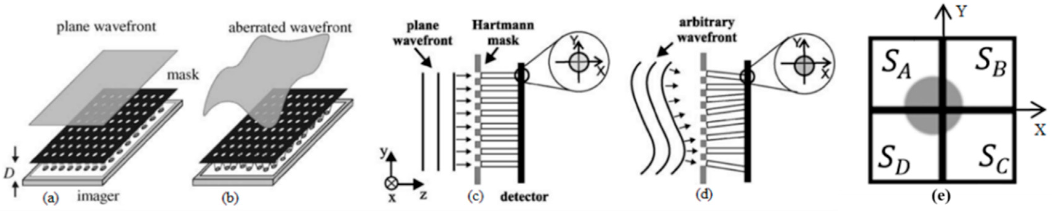
:1. Introduction
2. Simulation Method and Structure
3. Simulation Results
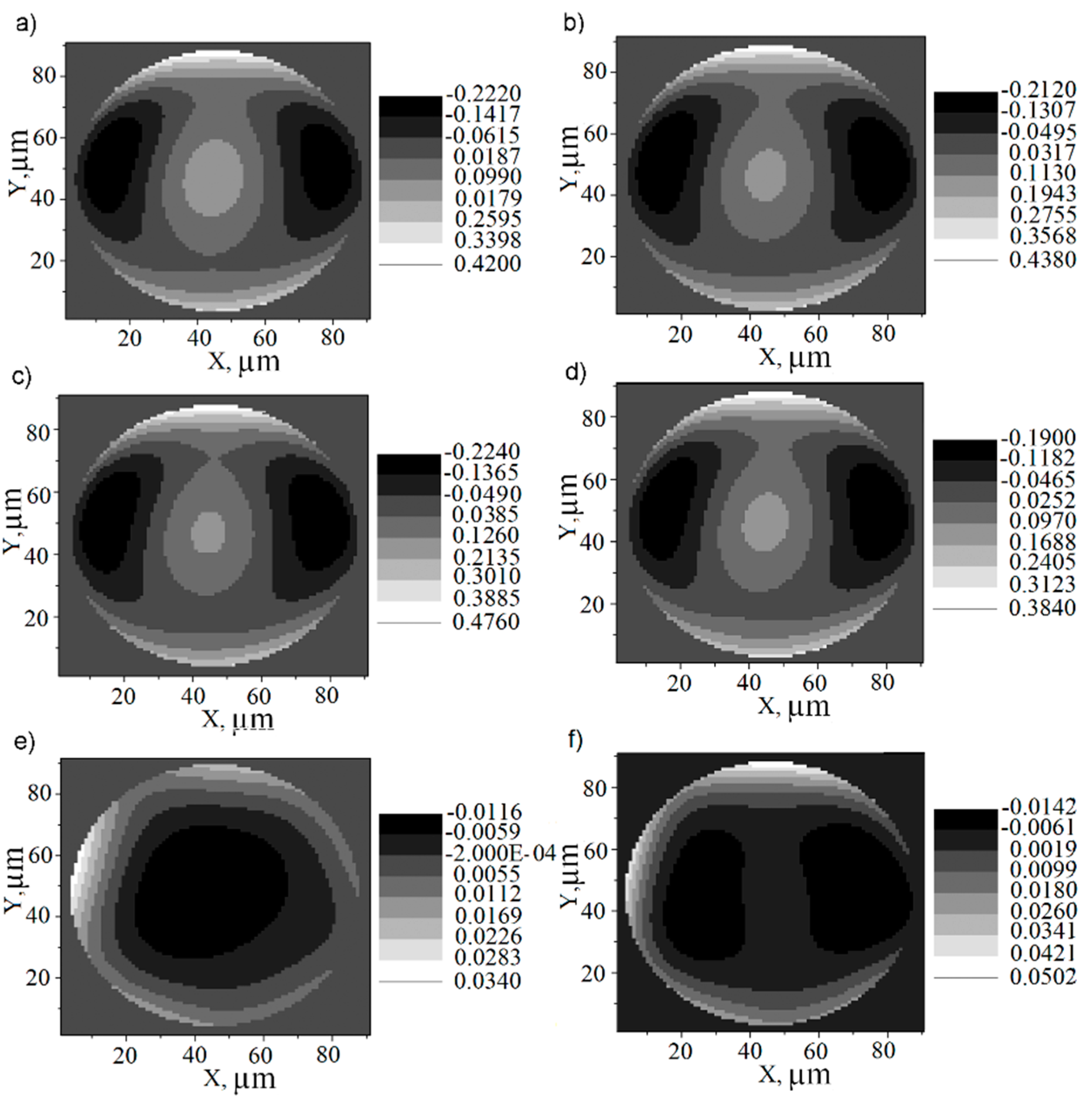
3.1. Considerations
3.2. Results
4. Conclusions
Author Contributions
Funding
Acknowledgments
Conflicts of Interest
Appendix A

| Symbol | Parameter | Simulation Value | Unit | Step |
|---|---|---|---|---|
| Λ | Operational wavelength | 0.633 | µm | 1 |
| Number of Zernike polynomial terms | 20 | - | 1 | |
| Quantity of microlenses in the microlens array | 25, 36, 49, 64, 81, 100 | - | 3 | |
| Dmicrolens | Diameter of each microlens | 1000 | µm | 3 |
| Lateral dimension of the microlens array | 6000 | µm | 3 | |
| F | Focal distance | 200,000 | µm | 3 |
| RQC | Dimension of a cell from the QC | 200 | µm | 4 |
| Spacing between QCs | 10 | µm | 4 | |
| rc | Central radius of the QCD | 0.325 RQC | µm | 4 |
| ηr | Relative quantum efficiency of the QCD | 0.667 | - | 4 |
| Reff | Spot effective radius | 0.30 RQC | µm | 4 |
| Linearization | 0.46 RQC | µm | 4 | |
| αm | Absorption coefficient of the material (Si) | 3345 | cm−1 | 4 |
| R | Reflectance | 0.1 | 4 | |
| Ln | Diffusion length of electrons | 87.68 × 10⁻⁶ | cm | 5 |
| Lp | Diffusion length of holes | 29.30 × 10⁻³ | cm | 5 |
| Dn | Diffusivity of electrons | 2.23 | cm2/s | 5 |
| Dp | Diffusivity of holes | 10.76 | cm2/s | 5 |
| SN | Surface recombination speed for carriers in the cathode | 70 | cm/s | 5 |
| SP | Surface recombination speed for carriers in the anode | 4000 | cm/s | 5 |
| Cj | Capacitance of the photodiode junction | 2 | pF | 5 |
References
- Tyson, R.K. Principles of Adaptive Optics, 4th ed.; CRC Press: Boca Raton, FL, USA, 2015. [Google Scholar]
- Park, S.P.; Chung, J.K.; Greenstein, V.; Tsang, S.H.; Chang, S. A study of factors affecting the human cone photoreceptor density measured by adaptive optics scanning laser ophthalmoscope. Exp. Eye Res. 2013, 108, 1–9. [Google Scholar] [CrossRef] [PubMed] [Green Version]
- Zawadzki, R.J.; Capps, A.G.; Kim, D.Y.; Panorgias, A.; Stevenson, S.B.; Hamann, B.; Werner, J.S. Progress on developing adaptive optics—Optical coherence tomography for in vivo retinal imaging: Monitoring and correction of eye motion artifacts. IEEE J. Sel. Top. Quantum Electron. 2014, 20, 322–333. [Google Scholar] [CrossRef] [PubMed]
- Laslandes, M.; Salas, M.; Hitzenberger, C.K.; Pircher, M. Increasing the field of view of adaptive optics scanning laser ophthalmoscopy. Biomed. Opt. Express 2017, 8, 4811–4826. [Google Scholar] [CrossRef] [PubMed]
- Basden, A.G.; Bharmal, N.A.; Jenkins, D.; Morris, T.J.; Osborn, J.; Peng, J.; Staykov, L. The Durham Adaptive Optics Simulation Platform (DASP): Current Status. SoftwareX 2018, 7, 63–67. [Google Scholar] [CrossRef]
- Reeves, A. Soapy: An adaptive optics simulation written purely in Python for rapid concept development. Adapt. Opt. Syst. 2016, 9909, 9909F. [Google Scholar]
- Carbillet, M.; Vérinaud, C.; Femenía, B.; Riccardi, A.; Fini, L. Modelling astronomical adaptive optics—I. The software package CAOS. Mon. Not. R. Astron. Soc. 2005, 256, 1263–1275. [Google Scholar] [CrossRef]
- Wang, L.; Ellerbroek, B. Fast End-to-End Multi-Conjugate AO Simulations Using Graphical Processing Units and the MAOS Simulation Code. In Proceedings of the Second International Conference on Adaptive Optics for Extremely Large Telescopes, Victoria, BC, Canada, 25–30 September 2011. [Google Scholar]
- Le Louarn, M.; Madec, P.Y.; Marchetti, E.; Bonnet, H.; Esselborn, M. Simulations of E-ELT telescope effects on AO system performance. Adapt. Opt. Syst. V 2016, 9909. [Google Scholar] [CrossRef]
- Conan, R.; Correia, C. Object-oriented Matlab adaptive optics toolbox. Adapt. Opt. Syst. IV 2014, 9148. [Google Scholar] [CrossRef]
- Ellerbroek, B.L. Linear systems modeling of adaptive optics in the spatial-frequency domain. J. Opt. Soc. Am. A 2005, 22, 310–322. [Google Scholar] [CrossRef]
- Jolissaint, L.; Véran, J.P.; Conan, R. Analytical modeling of adaptive optics: Foundations of the phase spatial power spectrum approach. J. Opt. Soc. Am. A 2006, 23, 382–394. [Google Scholar] [CrossRef]
- Rigaut, F.; van Dam, M. Simulating Astronomical Adaptive Optics Systems Using Yao. In Proceedings of the Third AO4ELT Conference, Firenze, Italy, 26–31 May 2013. [Google Scholar]
- Platt, B.C.; Shack, R. History and principles of Shack-Hartmann wavefront sensing. J. Refract. Surg. 2001, 17, 573–577. [Google Scholar]
- De Lima Monteiro, D.W. CMOS-Based Integrated Wavefront Sensor. Ph.D. Thesis, Delft University of Technology, Delft, The Netherlands, 2002. [Google Scholar]
- Liu, R.; Milkie, D.E.; Kerlin, A.; MacLennan, B.; Ji, N. Direct phase measurement in zonal wavefront reconstruction using multidither coherent optical adaptive technique. Opt. Express 2014, 22, 1619–1628. [Google Scholar] [CrossRef] [PubMed]
- Ye, J.; Wang, W.; Gao, Z.; Liu, Z.; Wang, S.; Benítez, P.; Miñano, J.C.; Yuan, Q. Modal wavefront estimation from its slopes by numerical orthogonal transformation method over general shaped aperture. Opt. Express 2015, 23, 26208–26220. [Google Scholar] [CrossRef] [PubMed]
- Bond, C.Z.; Correia, C.M.; Sauvage, J.F.; Neichel, B.; Fusco, T. Iterative wave-front reconstruction in the Fourier domain. Opt. Express 2017, 25, 11452–11465. [Google Scholar] [CrossRef] [PubMed]
- Visser, C.C.; Verhaegen, M. Distributed wavefront reconstruction using measurements of the spatial derivatives of the wavefront for real-time large scale adaptive optics control. In Proceedings of the 2014 European Control Conference (ECC), Strasbourg, France, 24–27 June 2014. [Google Scholar]
- Noll, R.J. Zernike polynomials and atmospheric turbulence. J. Opt. Soc. Am. 1976, 66, 207–211. [Google Scholar] [CrossRef]
- Salles, L.P.; de Lima Monteiro, D.W. Designing the response of an optical quad-cell as position-sensitive detector. IEEE Sens. J. 2010, 10, 286–293. [Google Scholar] [CrossRef]
- Costa, L.C.; de Mello, A.S.B.; Salles, L.P.; de Lima Monteiro, D.W. Comparative Analysis of 350 nm CMOS Active Pixel Sensor Electronics. In Proceedings of the 2015 30th Symposium on Microelectronics Technology and Devices (SBMicro), Salvador, Brazil, 31 August–4 September 2015. [Google Scholar]
- Retes, L.P.F.; Torres, F.S.; de Lima Monteiro, D.W. Evaluation of the full operational cycle of a CMOS transfer-gated photodiode active pixel. Microelectron. J. 2011, 42, 1269–1275. [Google Scholar] [CrossRef]
- de Lima Monteiro, D.W.; Vdovin, G.; Sarro, P.M. High-speed wavefront sensor compatible with standard CMOS technology. Sens. Actuators A Phys. 2004, 109, 220–230. [Google Scholar] [CrossRef]
- Porter, J.; Guirao, A.; Cox, I.G.; Williams, D.R. Monochromatic aberrations of the human eye in a large population. J. Opt. Soc. Am. 2001, 18, 1793–1803. [Google Scholar] [CrossRef]
- Coura, T.; Salles, L.P.; de Lima Monteiro, D.W. Quantum-efficiency enhancement of CMOS photodiodes by deliberate violation of design rules. Sens. Actuators A Phys. 2011, 171, 109–117. [Google Scholar] [CrossRef]
- de Moraes Cruz, C.A. Simplified Wide Dynamic Range CMOS Image Sensor with 3T APS Reset-Drain Actuation. Ph.D. Thesis, Universidade Federal de Minas Gerais, Belo Horizonte-MG, Brazil, 2014. [Google Scholar]
- Liu, W.X.; Jin, X.; Xi, X.; Chen, J.; Jeng, M.C.; Liu, Z.; Cheng, Y.; Chen, K.; Chan, M.; Hui, K.; et al. BSIM3v3.3 MOSFET Model. 2005. Available online: http://ngspice.sourceforge.net/external-documents/models/ bsim330_manual.pdf (accessed on 27 January 2017).
- De Oliveira, O.G.; de Lima Monteiro, D.W. Optimization of the Hartmann-Shack microlens array. Opt. Lasers Eng. 2011, 49, 521–525. [Google Scholar] [CrossRef]
- Salles, L.P.; De Oliveira, O.G.; De Lima Monteiro, D.W. Wavefront Sensor Using Double-efficiency Quad-cells for the Measurement of High-order Ocular Aberrations. In Proceedings of the 24th Symposium on Microelectronics Technology and Devices, Natal, Brazil, 31 August–3 September 2009. [Google Scholar]
- Malacara, D. Optical Shop Testing, 3rd ed.; Wiley: Hoboken, NJ, USA, 2007. [Google Scholar]


| Number of Microlenses | ||
|---|---|---|
| 25 | 17 | 15 |
| 36 | 41 | 12 |
| 49 | 211 | 122 |
| 64 | 392 | 271 |
| 81 | 571 | 504 |
| 100 | 197 | 153 |
© 2018 by the authors. Licensee MDPI, Basel, Switzerland. This article is an open access article distributed under the terms and conditions of the Creative Commons Attribution (CC BY) license (http://creativecommons.org/licenses/by/4.0/).
Share and Cite
Abecassis, Ú.V.; De Lima Monteiro, D.W.; Salles, L.P.; De Moraes Cruz, C.A.; Agra Belmonte, P.N. Impact of CMOS Pixel and Electronic Circuitry in the Performance of a Hartmann-Shack Wavefront Sensor. Sensors 2018, 18, 3282. https://doi.org/10.3390/s18103282
Abecassis ÚV, De Lima Monteiro DW, Salles LP, De Moraes Cruz CA, Agra Belmonte PN. Impact of CMOS Pixel and Electronic Circuitry in the Performance of a Hartmann-Shack Wavefront Sensor. Sensors. 2018; 18(10):3282. https://doi.org/10.3390/s18103282
Chicago/Turabian StyleAbecassis, Úrsula Vasconcelos, Davies William De Lima Monteiro, Luciana Pedrosa Salles, Carlos Augusto De Moraes Cruz, and Pablo Nunes Agra Belmonte. 2018. "Impact of CMOS Pixel and Electronic Circuitry in the Performance of a Hartmann-Shack Wavefront Sensor" Sensors 18, no. 10: 3282. https://doi.org/10.3390/s18103282