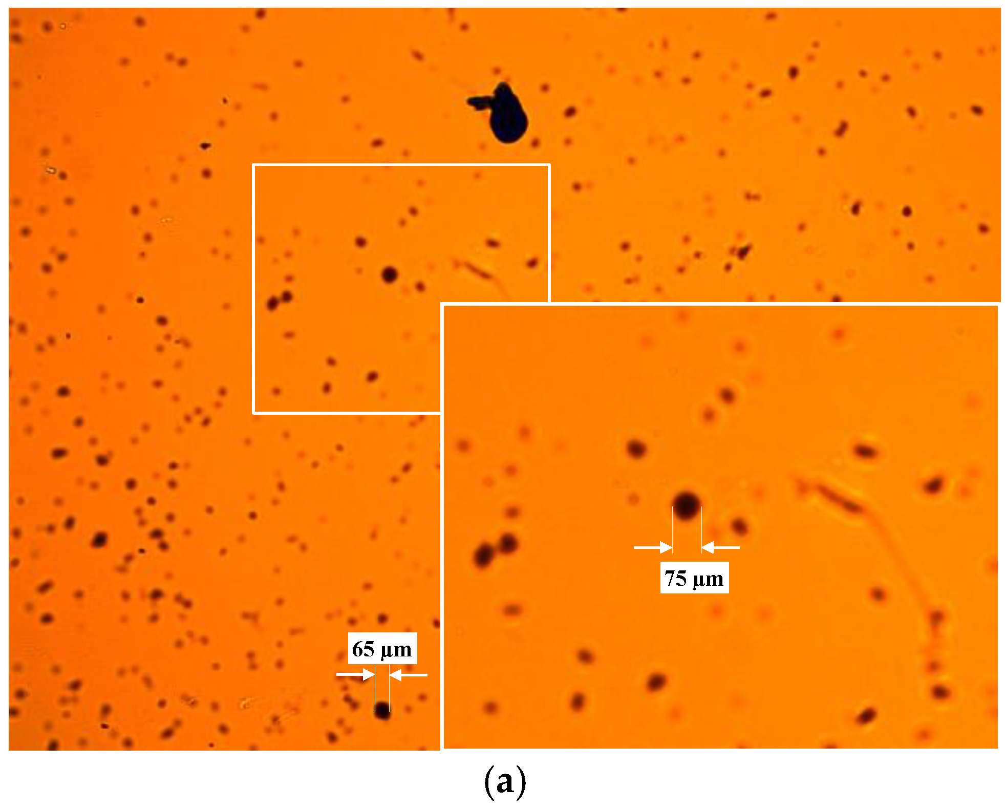
The results accomplished during the experiments at the optical test bench were considered promising enough for launching the design of the proof-of-concept sensor prototype.
3.2. Mechanics and Optical Design
The conclusions regarding FOV, Z
1, Z
2 and D
pinhole dimensions were fed into the specifications for mechanical design of the sensor body. Matching these micro-scale requirements with relatively challenging pressures (e.g., 10–15 bar), flows (e.g., 1–3 liter/min), viscosities (e.g., 320–480 cSt), etc. requires a careful system design. For instance, the requirement for using standardized hydraulic fast plug connectors (BSP Gas 1/8) in combination with the design target of reducing Z
2 as much as possible (~0.5 mm) has required to introduce crosswise sample inlet and outlets, due to space restrictions, as it can be observed in
Figure 14.
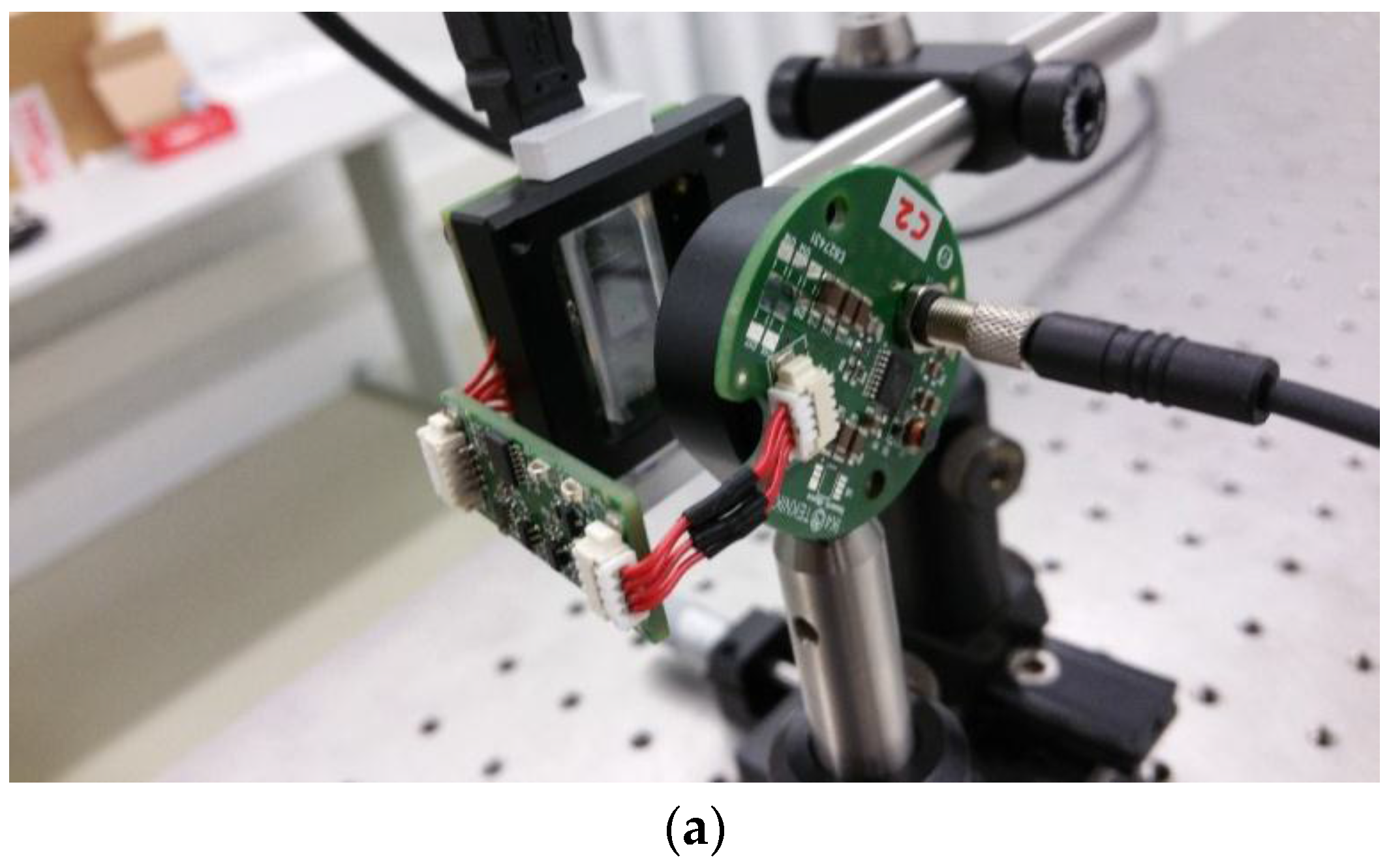
Integrating the electronics, mechanics and optics, the sensor dimensions are approximately 35 × 45 × 45 mm, which could be considered as a very compact solution. The sensor body is fabricated in anodized aluminum and the sealing materials are fluorocarbons (for mineral or synthetic lubricant fluids) or EPDM (for measuring phosphate ester-based hydraulic fluids). Regarding the optical window closest to the CMOS sensor, which defines the Z
2 distance, it should be keep the thinnest possible while standing the fluid pressure specification. The following formula describes the minimum thickness of glass disk before it breaks under a given pressure:
Whereas, T represents the minimum thickness in inches, A defines the unsupported area in sq/inches, P is the maximum pressure in psi, M defines the modulus of rupture (in psi) and F is a safety factor that normally is set to 7. Therefore, depending on the type of glass, different thickness could be used for tolerating a specified maximum pressures of 10 bars. In the current proof of concept, two different glass materials and thicknesses have been used. The first option is a 0.2 mm ultra-thin BK7 (M ~2400 psi) window from Edmund Optics (Barrington, NJ, USA), that have been selected with the aim of demonstrating the best optical performance as it allows a high reduction in the Z2 distance. Unfortunately, according to Equation (6), this BK7 option only bears 0.01 bars, meaning that its use is restricted to low pressure applications. The second candidate is a 1.1mm thick Gorilla® Glass (M ~100,000 psi) disk, which allows working up to 11 bars but sets Z2 a little bit further, but still in the range of operation for incoherent lens-less applications. The second optical window (the one closest to the pinhole) has been resolved with a thicker BK7 glass disk (3 mm). The sample path is 0.5 mm, equivalent to tests performed with the cuvettes.
Additionally, in order to protect the CMOS sensor from the bending occurring at the glass window, a small security air gap of 0.2 mm has been defined. Therefore, the system is able to offer a minimum Z2 of 0.4 mm mounting the ultrathin glass disk and a maximum of Z2 1.3 mm when using the Gorilla® glass. Implementing the Z1 distance is much straightforward, and the sensor integrates a mechanical solution for holding the pinhole plate at 10 mm from the center of the sample path.
3.3. Light System Design
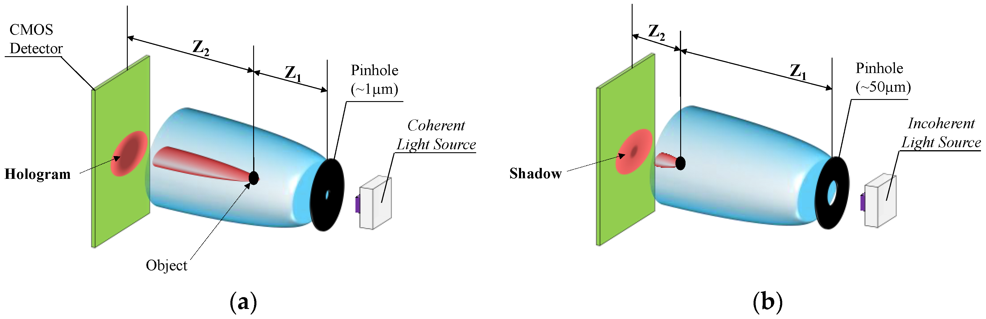
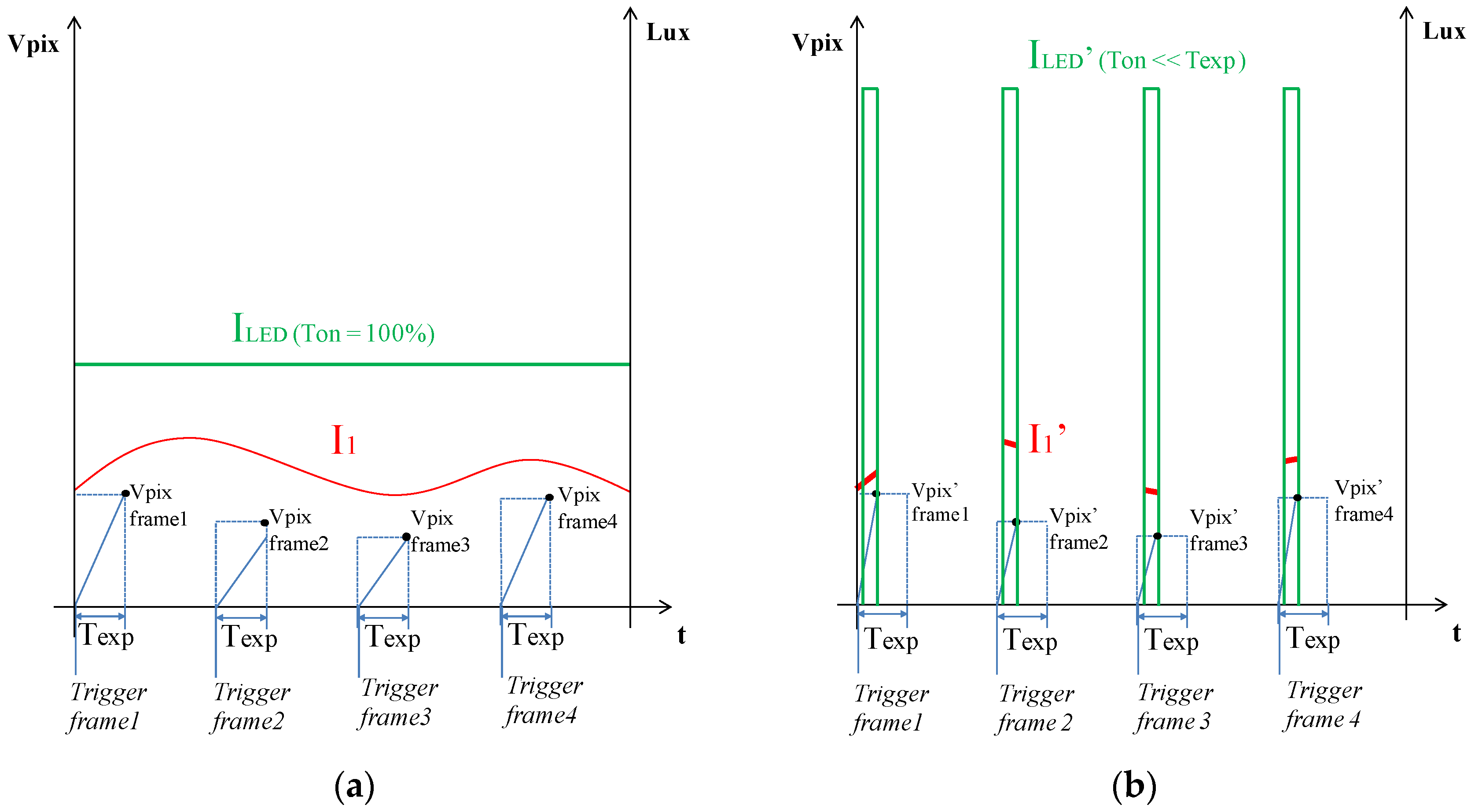
Pinhole selection and the light emitter design has been driven by the light power requirements for properly illuminating flowing lubricants. As it has been explained in earlier sections, due to the instant velocity of the particulate flowing within the lubricant, a stroboscopic lighting system is required for avoiding the generation of distorted images. In this context, the duration of these pulses is defined by the expected velocity of the objects (particles) suspended in the fluid under supervision when they go through the focusing area of the CMOS. Indeed, the duration of the illumination pulse is inversely proportional to the maximum velocity of the moving objects.
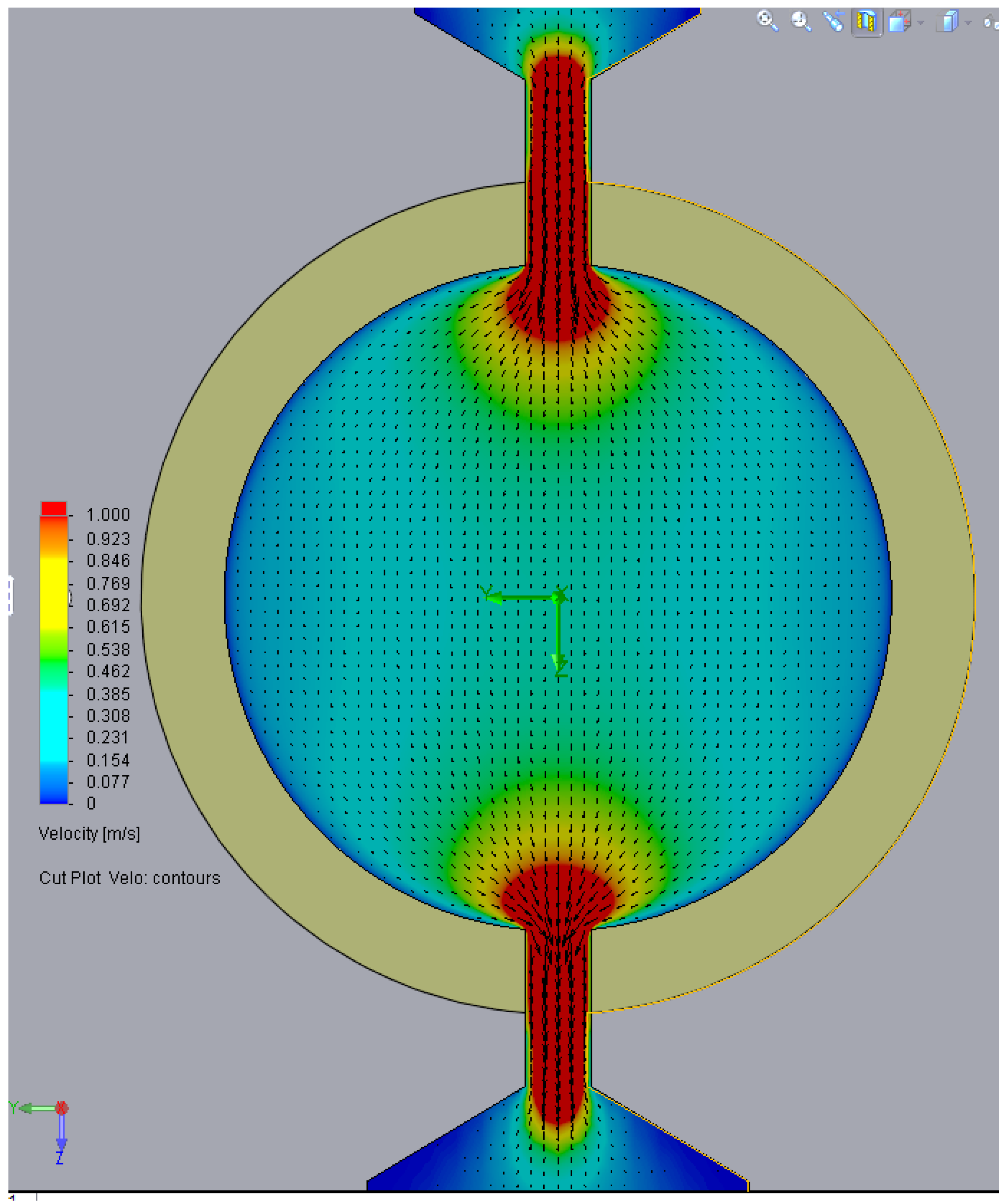
According to the Computational Fluid Dynamics (CFD) simulation displayed in
Figure 15, considering a range of working pressures of 2, 5 and 10 bars, the expected laminar flow speeds of the lubricant across the microfluidic structure of the sensor are 3, 11 and 22 m/s, respectively. Therefore, the particulate suspended in the fluid will also move at similar velocities (not considering turbulence effects, etc.).
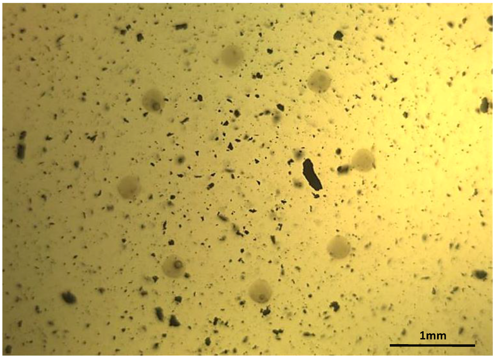
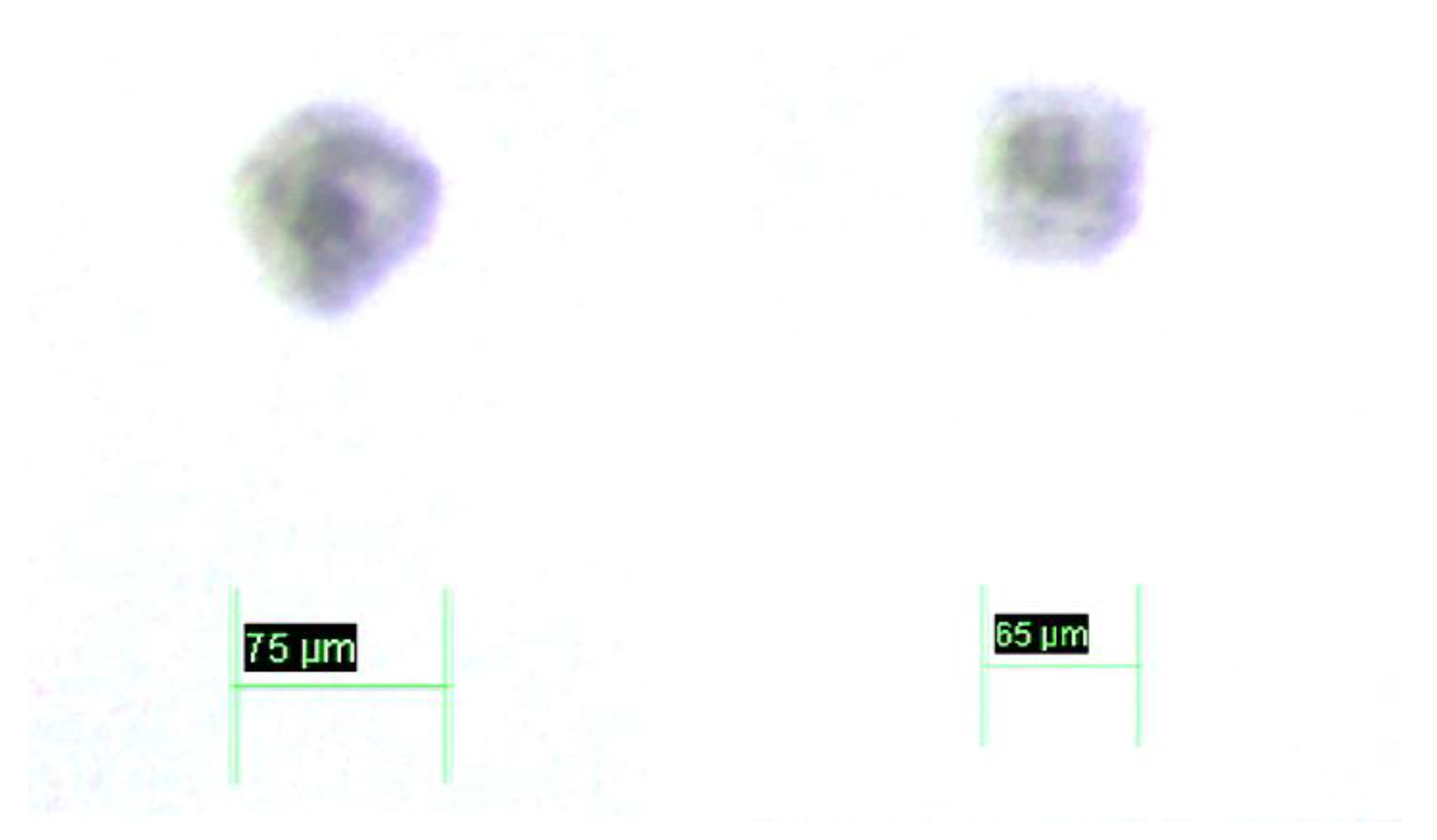
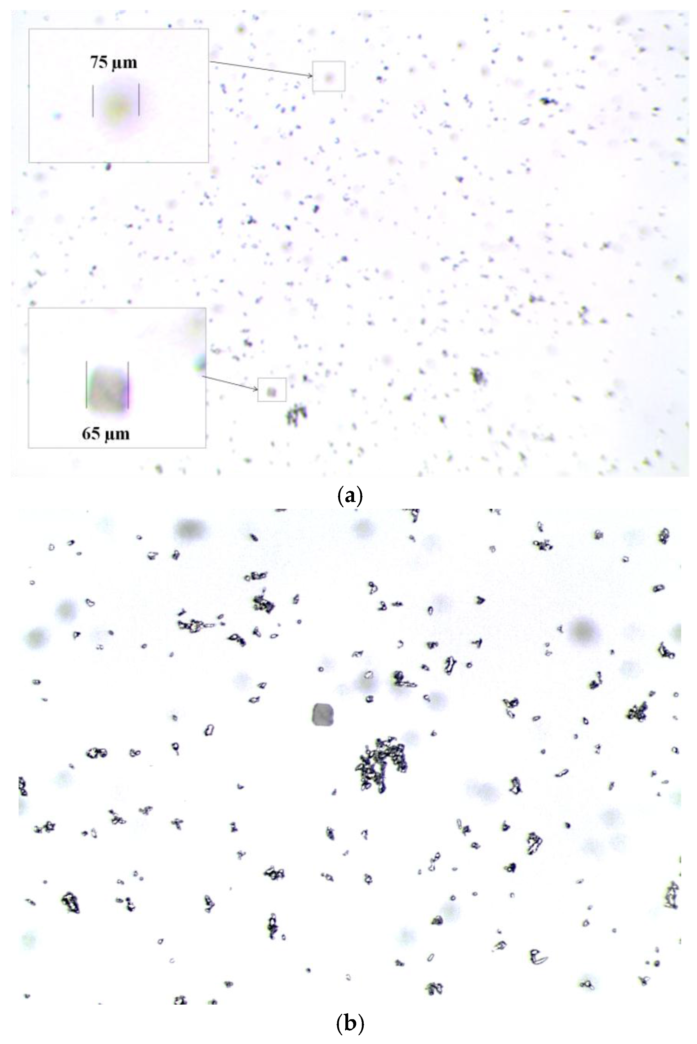
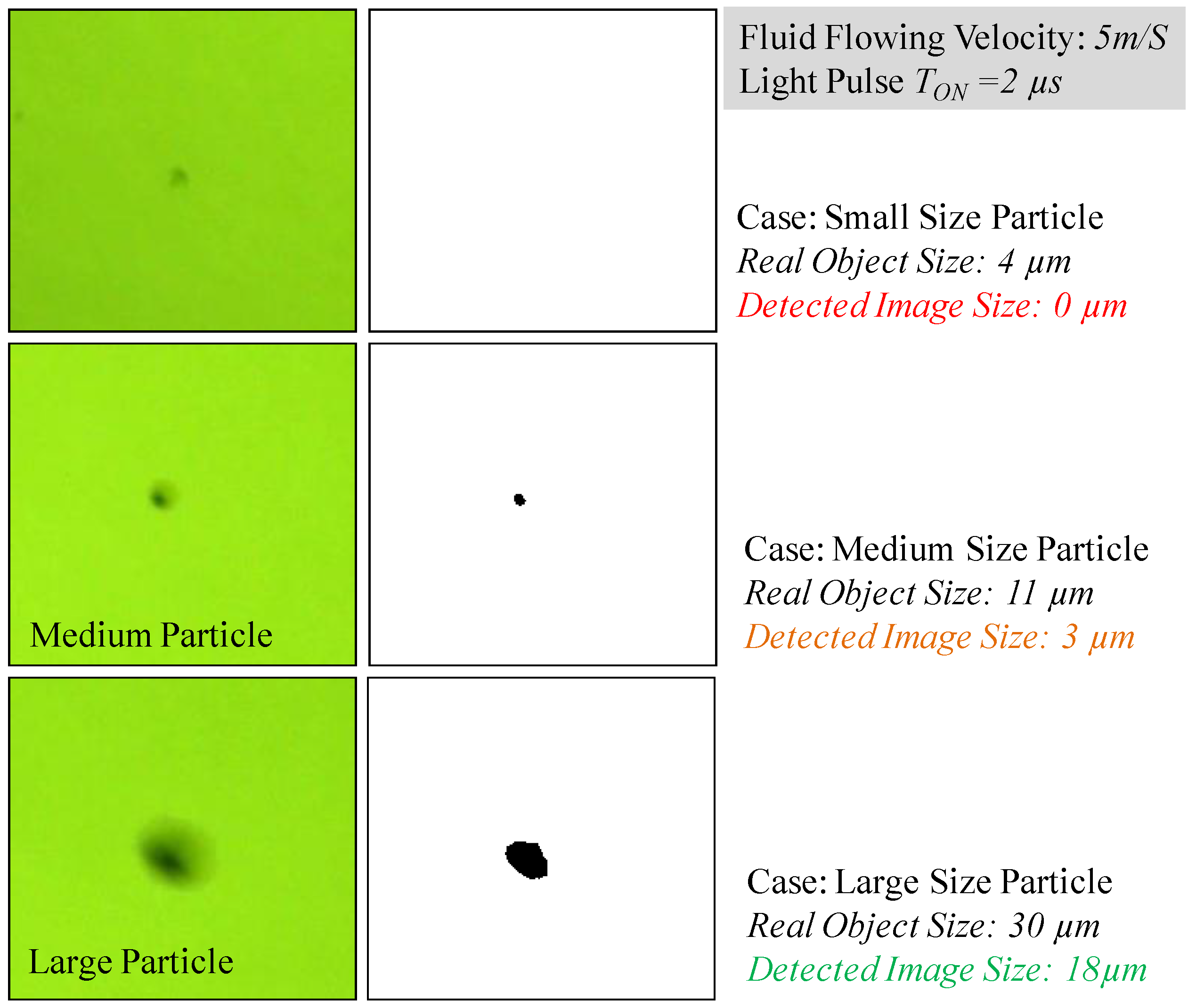
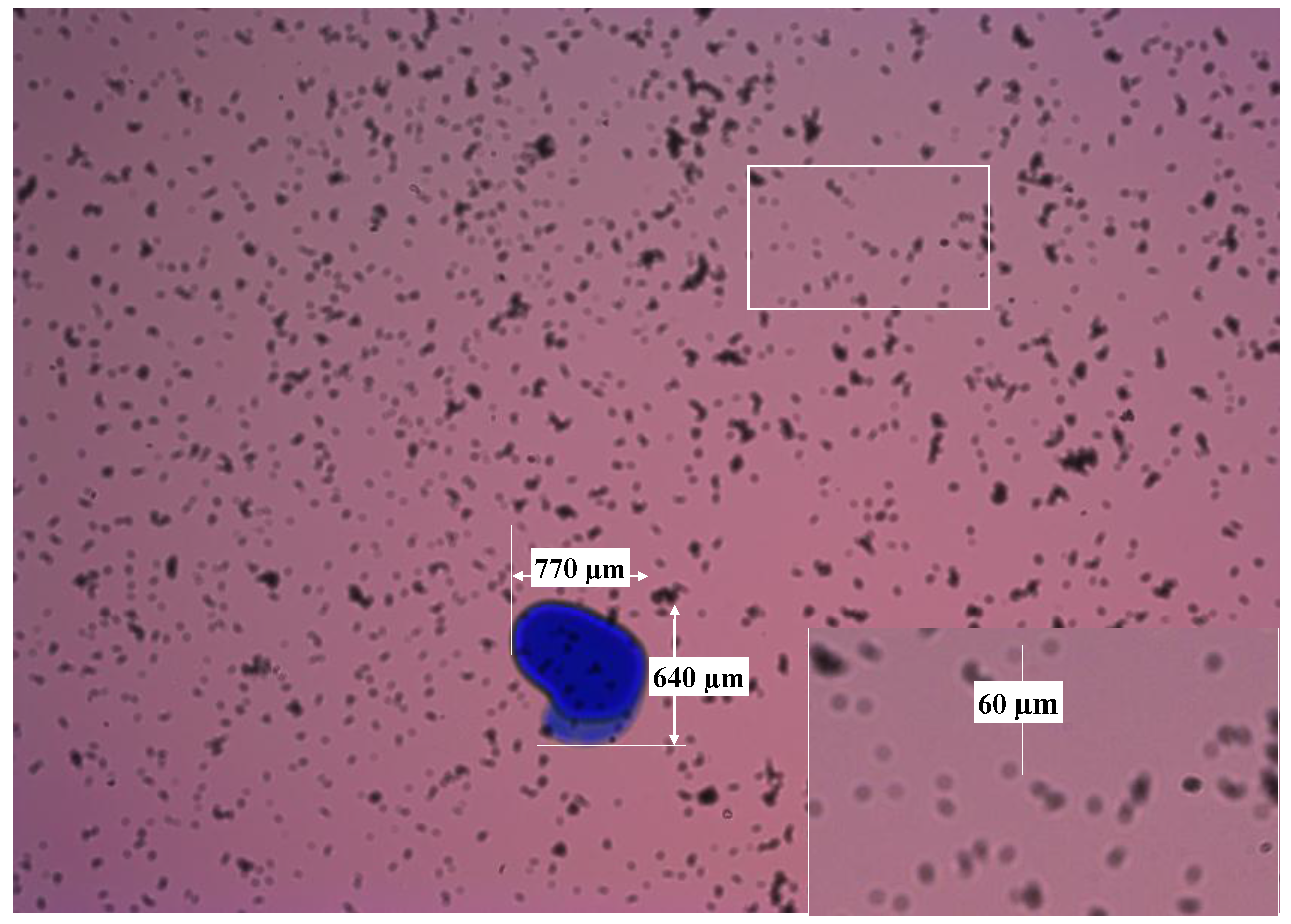
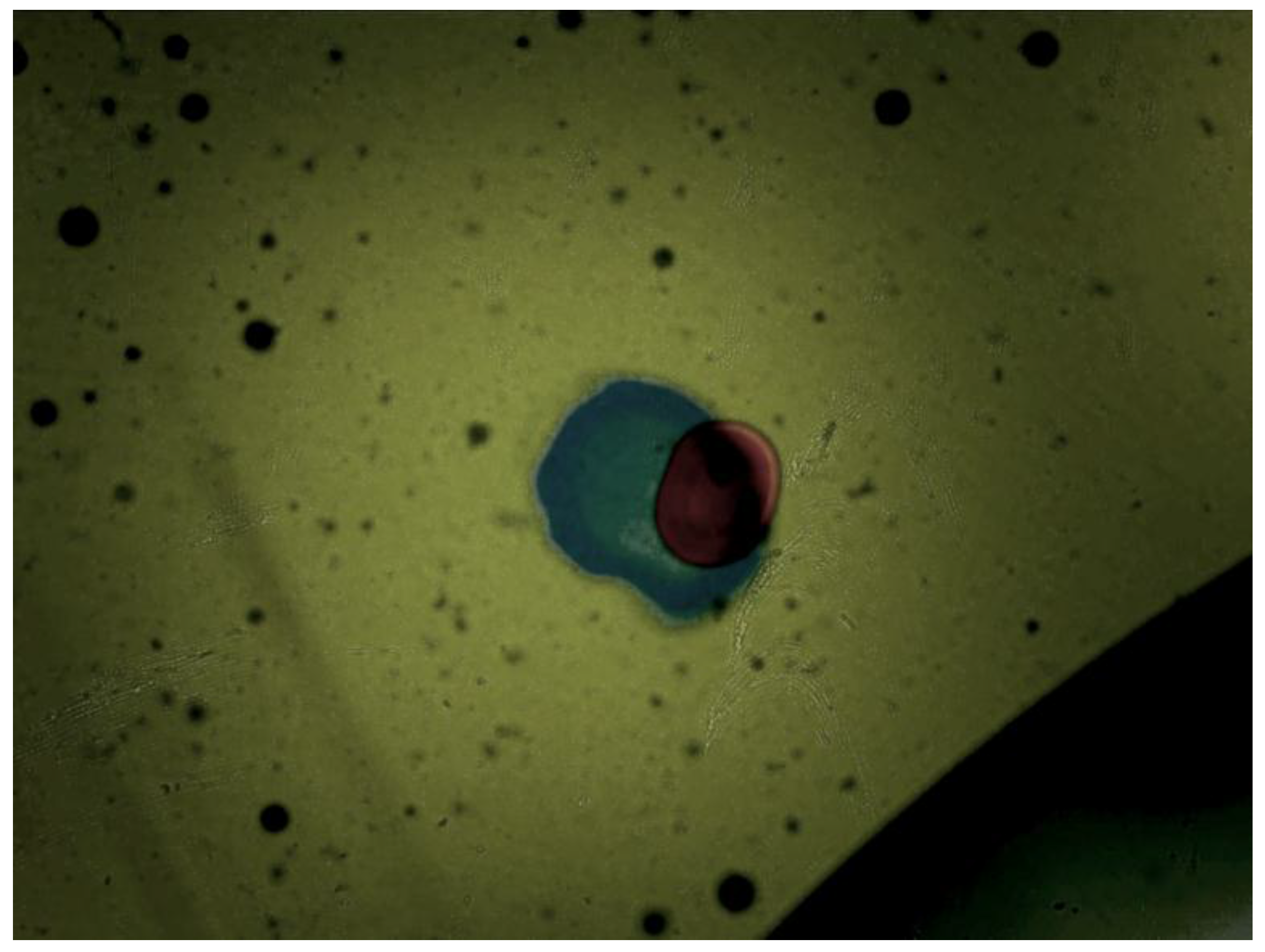
However, even if all particles are moving at the same velocity, the effect of the image capture distortion does not affect large and small particles alike. Large particles, even with a small distortion, will be detectable by the machine vision algorithms and there is no significant impact, being the real particle size very close to the size of the object detected. However, as the particle size gets smaller, the effects of the distortion are more pronounced, impacting both on the size and on its apparent shape, even making the smallest particles non-perceptible for the detection algorithms, as it can be observed in the example displayed in
Figure 16.
In this situation, a criterion has been defined to determine which percentage of distortion generates a fatal impact for the particle detection. Considering for example that distortion will cause a bad detection if 50% of the area of the object is affected, the
Table 2 shows the maximum duration of the stroboscopic light pulse for different object sizes (largest dimension) and velocity of the fluid, calculated as:
The time lapse limits the interval of time that a particle of a certain size could be moving without generating a distortion that would impact on its later recognition. Therefore, this interval defines the maximum allowed pulse duration, TON, for the stroboscopic lighting system.
With such a little time (e.g., 500 ns < T
ON < 4 μs) for illuminating the fluid sample, it is straightforward to conclude that a high-power light source will be required for generating a decent signal level at the detector; moreover considering the current responsivity or sensitivity of industrial CMOS with 2.2 μm
2 pixel sizes is approximately 1 to 2 V/Lux-s (e.g., MT9P006 sensor features 1.76 V/Lux-s and the AR0330 1.9 V/Lux-s at λ = 550 nm). If generating a mid-scale intensity value at each pixel of the CMOS is set as the design objective, the light intensity budget calculation across the system could be approximately described with the following equations and considerations:
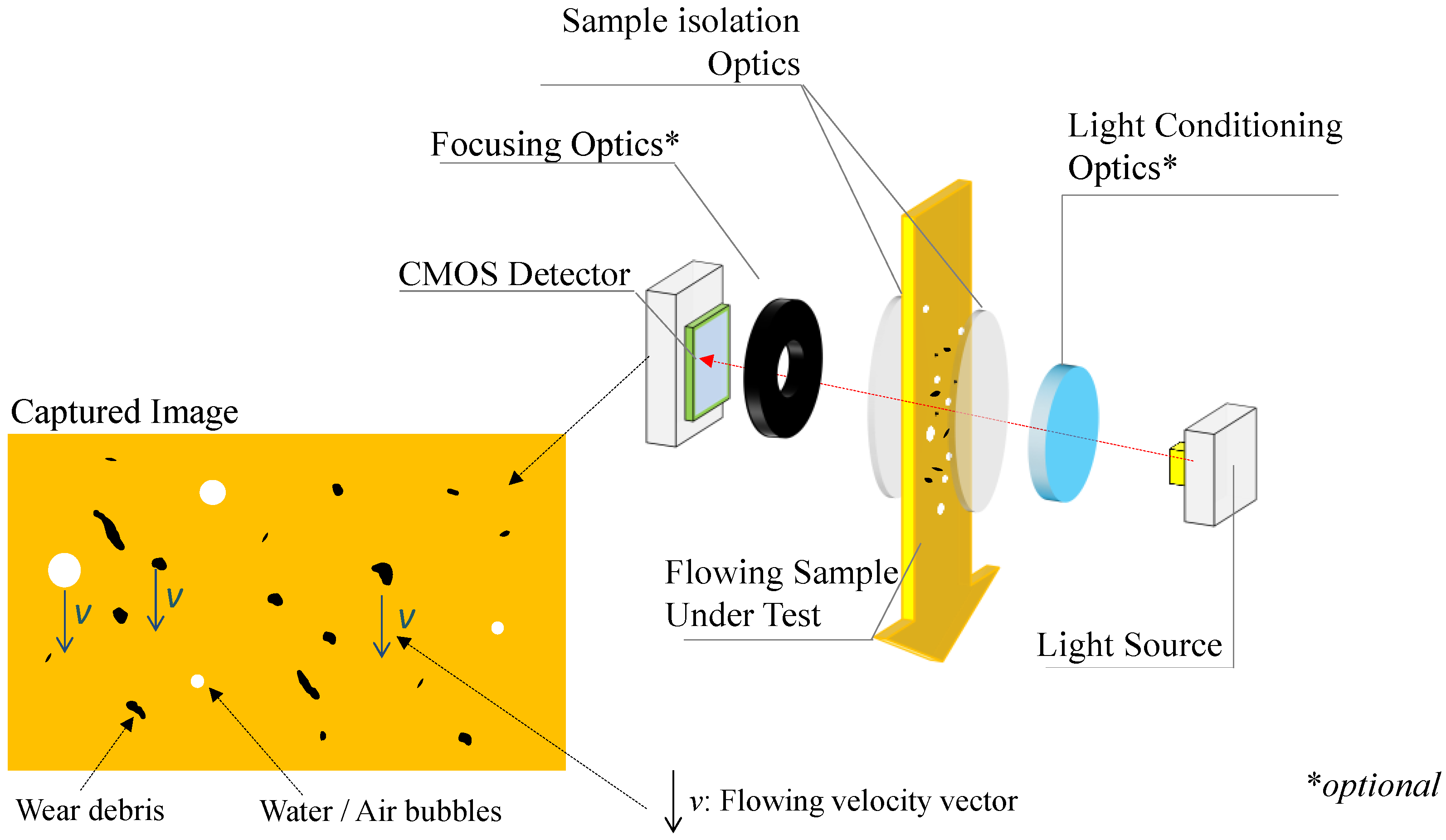
Therefore, sufficient light energy needs to be provided by the system to allow that light flux getting to each pixel. The diagram depicted in the
Figure 8, describes the different main considerations for the light power budget required for the current application as the light absorption happening at the sample, free space losses and the light filtering occurring at the pinhole.
Considering that the absorptions across the free space (FSPL) and at the cuvette walls are both negligible, then, the most important factors for the light intensity losses are the absorption happening at the fluid sample and the light filtering at the pinhole. Friss Formula, which describes free space power losses as FSPL = (4π × D/λ)
2, allows us to demonstrate the assumption of FSPL~0, being D~Z
1~0.01 m or D~Z
2~0.001 m. In addition, the high transmission of the quartz (above %90) across the visible light spectrum [
41], demonstrates the low impact of the glass disks in the light intensity budget. Therefore, we assume that I
pinhole~I
0 and I
1~I
PIXEL.The absorption of the light crossing through the sample fluid is defined by the Lambert-Beer law, which describes an exponential relation between the light entering the sample (I
0) and the light getting across it (I
1) as I
1 = I
0 × 10
− εℓc = I
0 × 10
−A, whereas
ε is the attenuation coefficient;
c is the amount concentration of the absorbent; and
ℓ is the path length of the beam of light through the fluid sample; and their product represents the absorptivity (
A) happening at the sample.
A value of
A = 0.5 is taken as an average absorptivity of used lubricant oil at ʎ
0 = 580 nm for 0.5 mm path length [
42,
43], accordingly, the incoming light power will be lowered in a factor of: 10
−A = 10
−0.5 = 0.316. Therefore:
and from Equation (12):
At this point, the ILED to Ipinhole relation needs to be defined to calculate the minimum light power that needs to be generated by the illumination solution to deliver an image on the camera sensor with decent brightness. As the aperture could be considered as an spatial filter that blocks a significant portion of the emitted light flux, it is straightforward to correlate the light power transmitted through the pinhole with the area of the aperture (Ipinhole∝ Dpinhole).
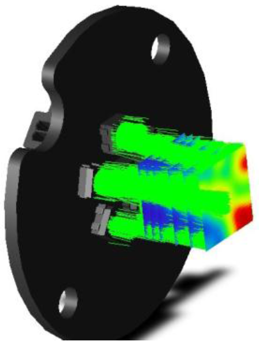
Based on the output from ZEMAX simulation (see
Figure 17), a set of six LEDs have been validated for illuminating the pinhole from a distance of ~5 mm within a polished aluminum case. The white LEDs chosen offer a light flux of 178 lumens/W (9 W maximum) at 120° viewing angle. This means, that at a 5 mm distance, the illumination system, per each LED, is able to generate approximately 2,266,000 Lux/W spread following a Gaussian distribution in an area of 235 mm
2 right before the pinhole. However, only a minimal proportion of this light flux will get across the aperture, and could be described as:
Combining Equation (16) with Equation (13), I
PIXEL is defined in dependence with the polarization of the LED and with the diameter of the pinhole:
Then, for each of candidate pinholes, different LED number and polarization currents are needed for achieving the targeted mid-scale intensity level of IPIXEL = Lux. If the saturation current is reached, and considering a fixed number of LEDs (a circular array of 6 LEDs have been arranged for the current setting), we would be forced to increase the stroboscopic pulse time above the cited 4 µs.
As mentioned, due to the pinhole filtering, only a small proportion of this light beam power will be transmitted to the sample.
Table 3 summarizes the expected light power at the pixel plane considering all the assumptions and design parameters described so far. The data displayed concludes that the only feasible pinhole diameter is the 500 μm for the target fluid absorptivity and fluid flowing velocity, because it is the only setting that enables achieving the requested design objective of I
PIXEL of
.
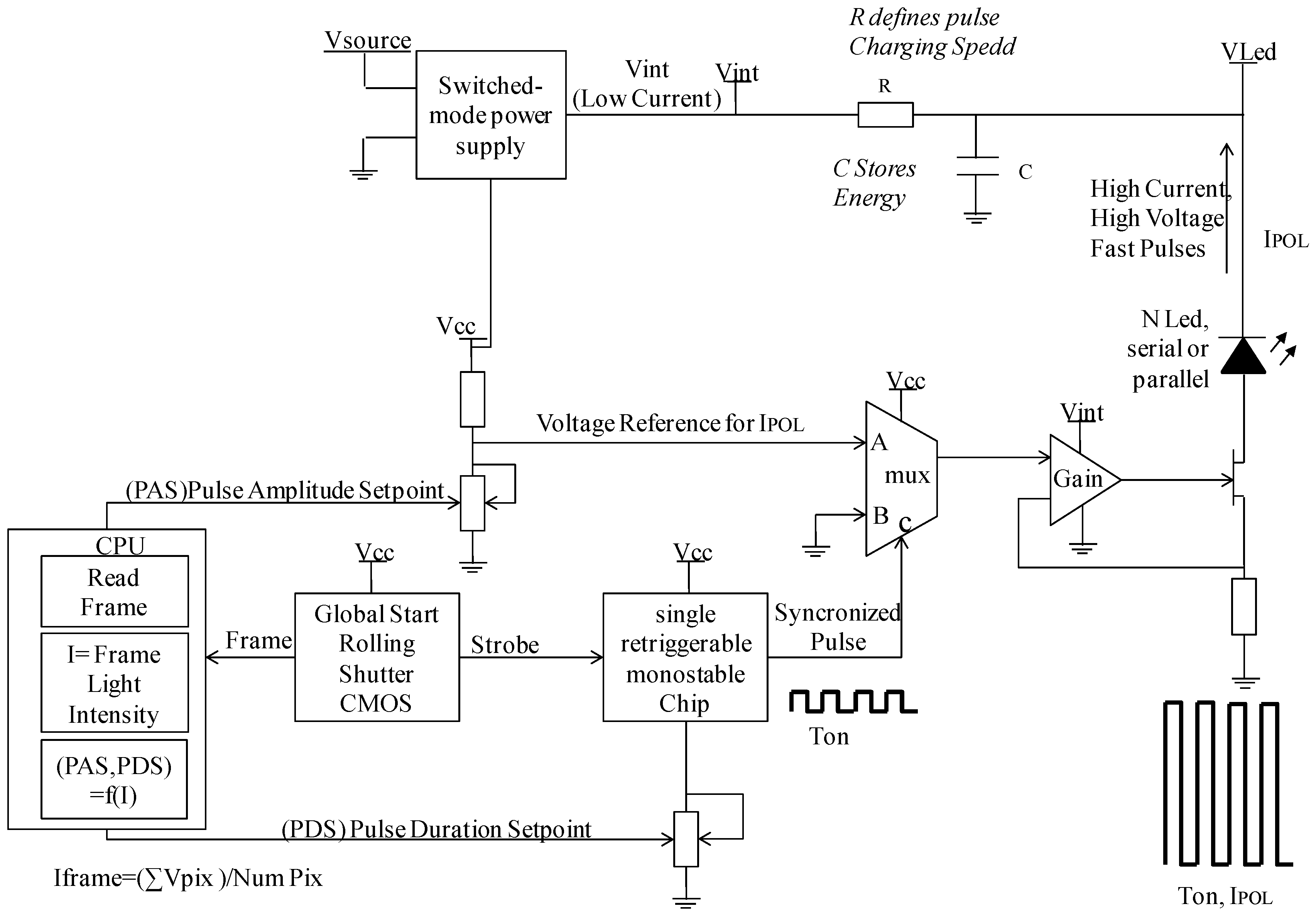
A custom circuit has been designed for controlling the pulse length and intensity of the LEDs using an algorithm that is executed on the CPU. The activation time (T
ON) and polarization current (I
0) of the LEDs for achieving the frame intensity set point is computed for every new frame. As depicted in the
Figure 18, a capacitors array is used for storing the energy required for driving the LEDs. This setup allows meeting the requirement of a very fast (T
RISE < 10% T
ON) pulse switching times even for very short pulses, which is a critical design challenge, as described in [
44,
45].


