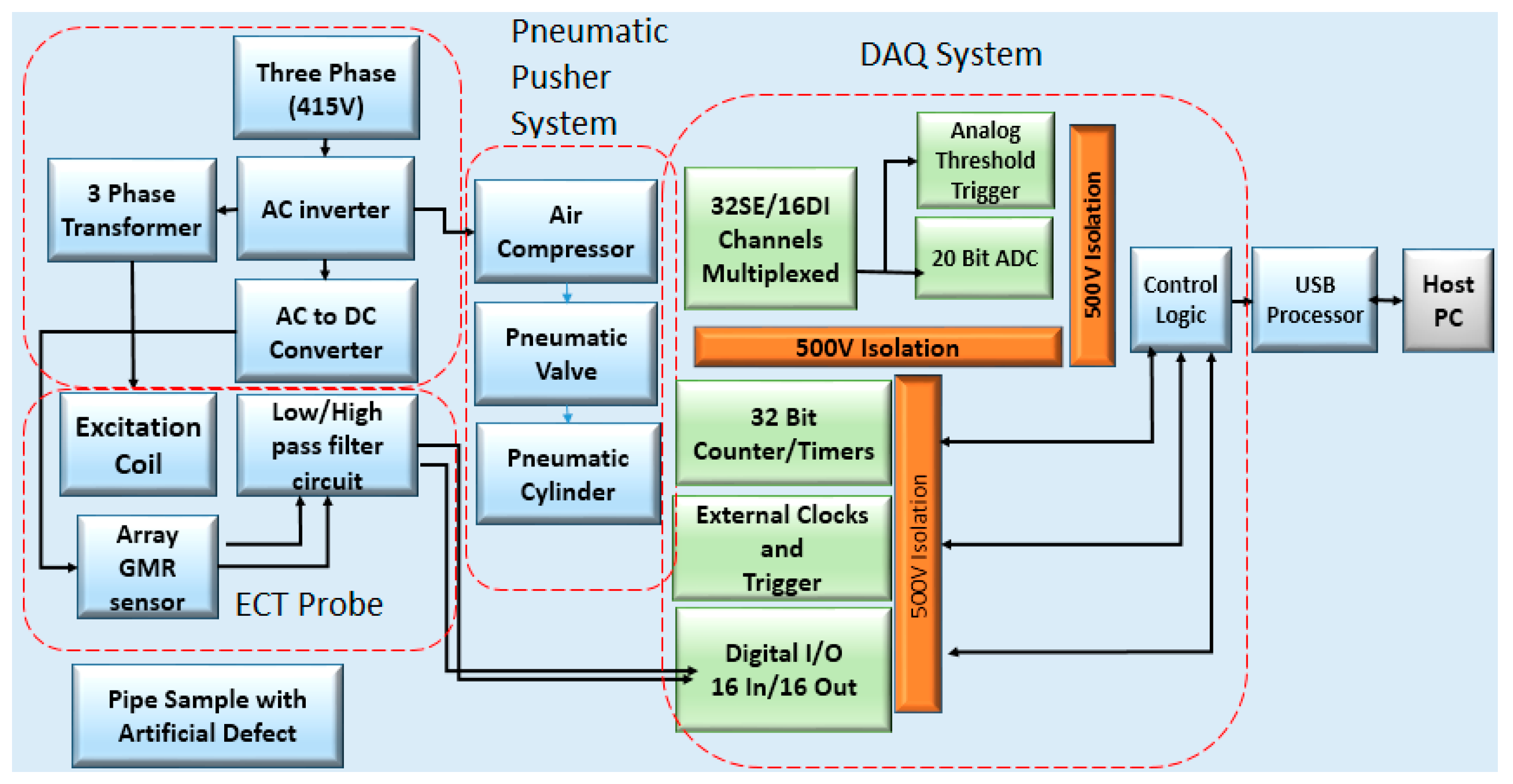
Figure 1.
Architecture of Distributed System for Eddy Current Testing (DSECT).
Figure 1.
Architecture of Distributed System for Eddy Current Testing (DSECT).
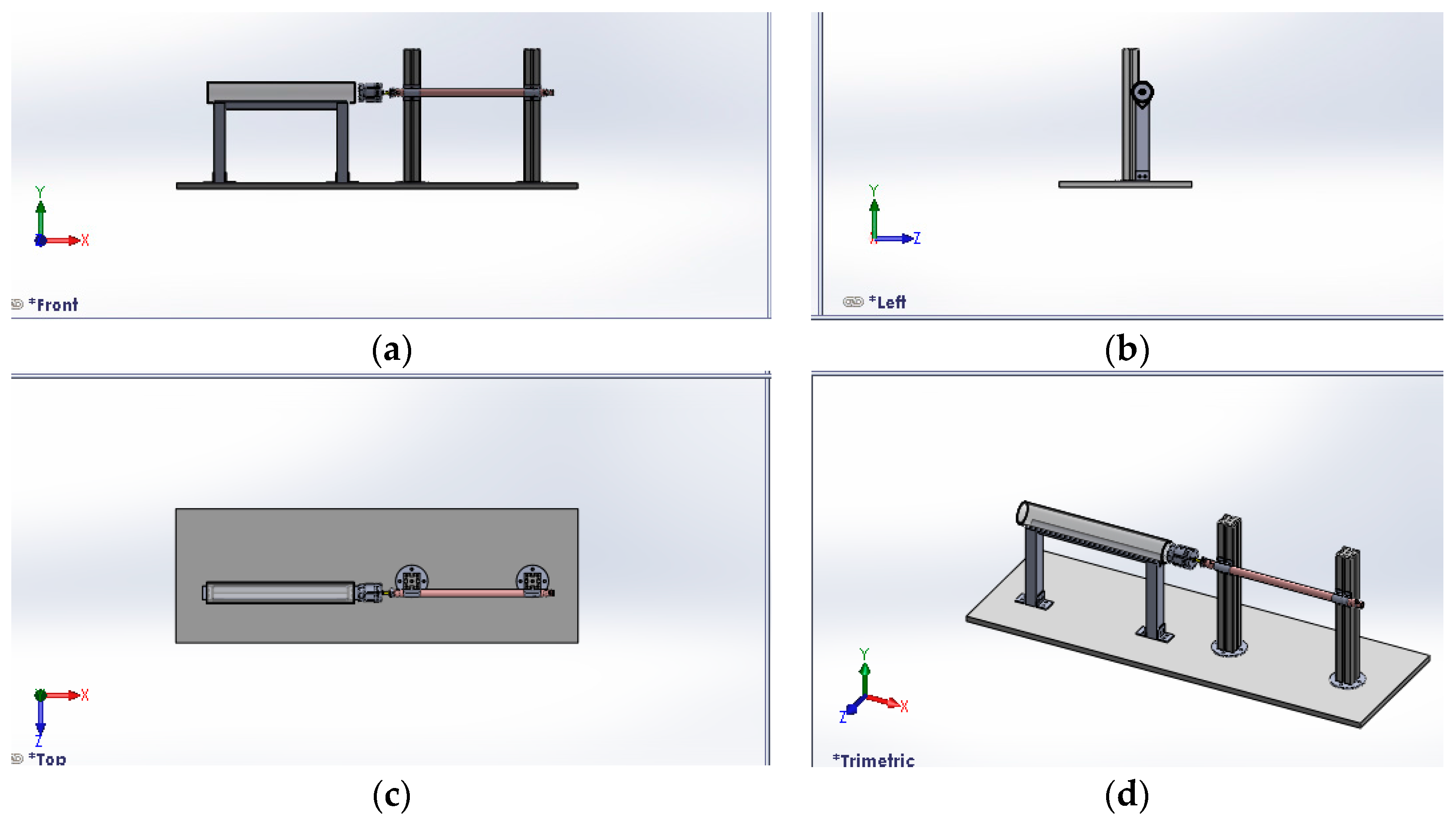
Figure 2.
Design of the Distributed System for Eddy Current Testing (DSECT) (a) Front view (b) Side view (c) Top view (d) Angle view.
Figure 2.
Design of the Distributed System for Eddy Current Testing (DSECT) (a) Front view (b) Side view (c) Top view (d) Angle view.
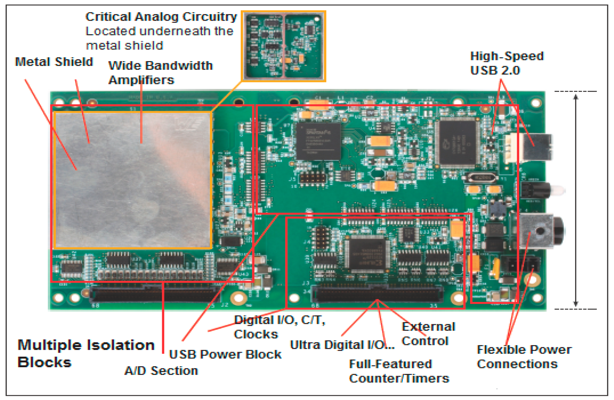
Figure 3.
High-speed DAQ card (DT 9844) for the DSECT system.
Figure 3.
High-speed DAQ card (DT 9844) for the DSECT system.
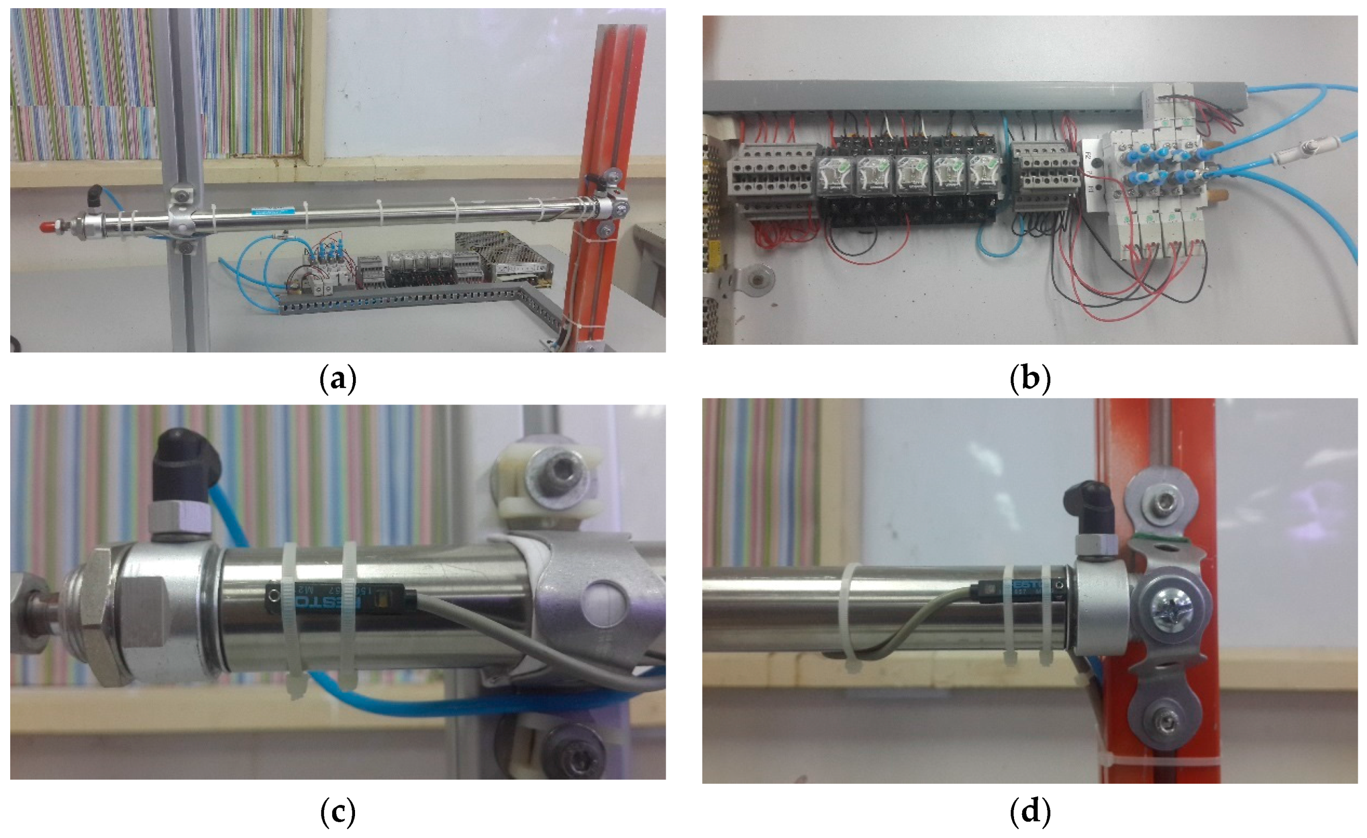
Figure 4.
DSECT Pusher system (a) Hardware setup (b) Pneumatic system (c) Festo magnetic reed sensor at the end of cylinder (d) Festo magnetic reed sensor at the beginning of cylinder.
Figure 4.
DSECT Pusher system (a) Hardware setup (b) Pneumatic system (c) Festo magnetic reed sensor at the end of cylinder (d) Festo magnetic reed sensor at the beginning of cylinder.
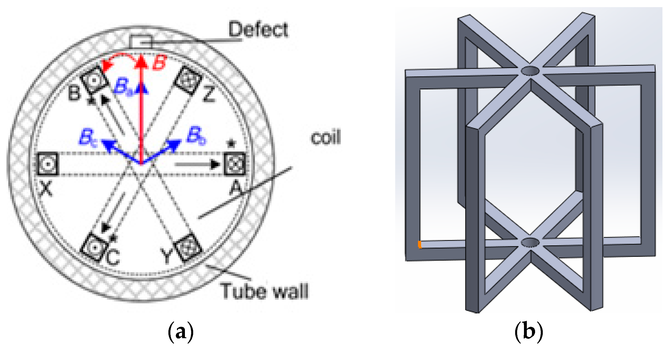
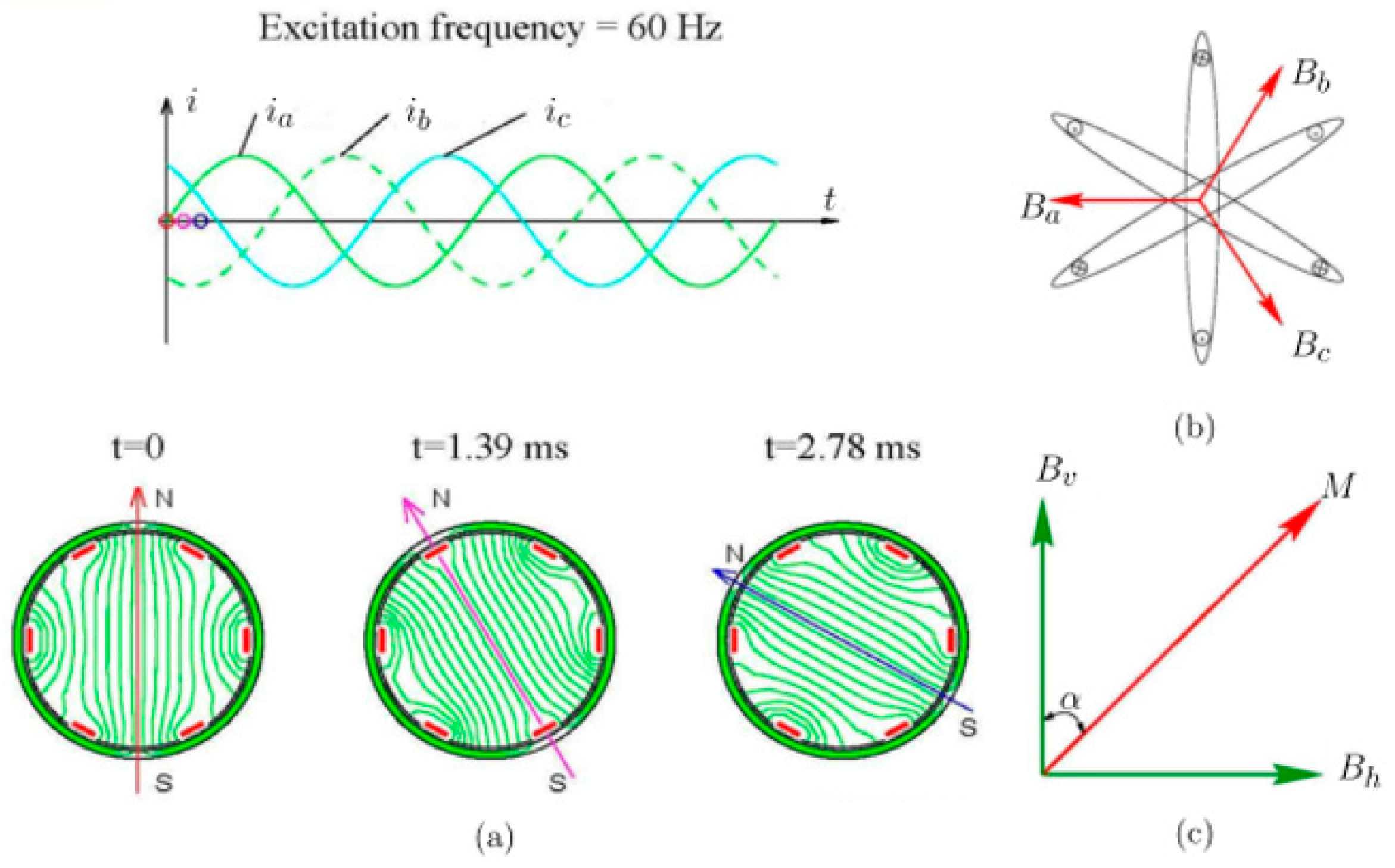
Figure 5.
Principle of the rotating field: (a) three-phase currents (b) flux due to currents in three-phase winding (c) horizontal and vertical components of the resultant magnetic flux.
Figure 5.
Principle of the rotating field: (a) three-phase currents (b) flux due to currents in three-phase winding (c) horizontal and vertical components of the resultant magnetic flux.
Figure 6.
Rotating field windings and bobbin pickup coil: (a) Three phase excitation windings; (b) 3D model of three coils winding for probe excitation.
Figure 6.
Rotating field windings and bobbin pickup coil: (a) Three phase excitation windings; (b) 3D model of three coils winding for probe excitation.
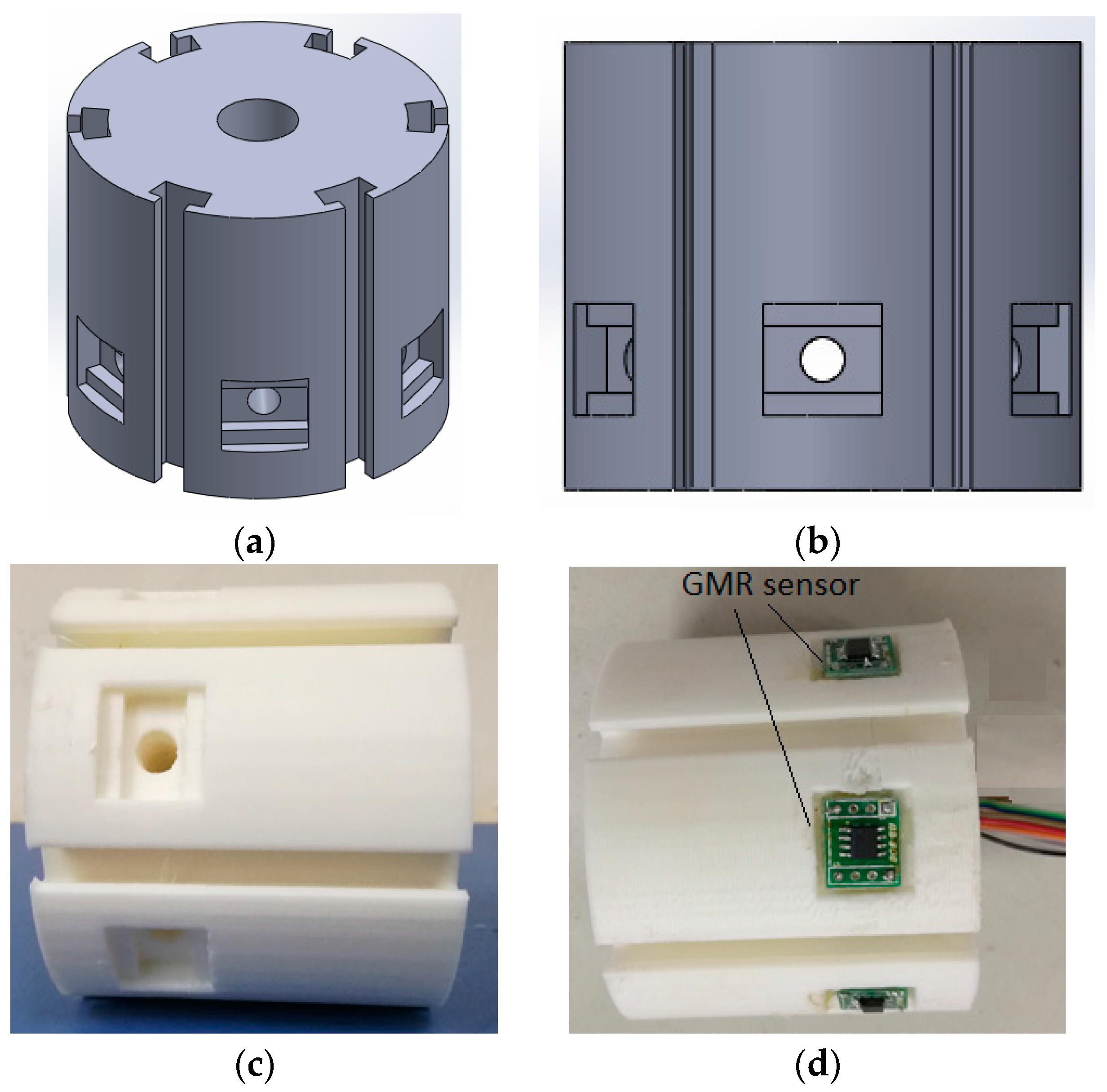
Figure 7.
Proposed ECT probe design for DSECT system: (a) trimetric view (b) left view (c,d) probe prototype.
Figure 7.
Proposed ECT probe design for DSECT system: (a) trimetric view (b) left view (c,d) probe prototype.
Figure 8.
Magnetic flux density decay along diameter direction.
Figure 8.
Magnetic flux density decay along diameter direction.
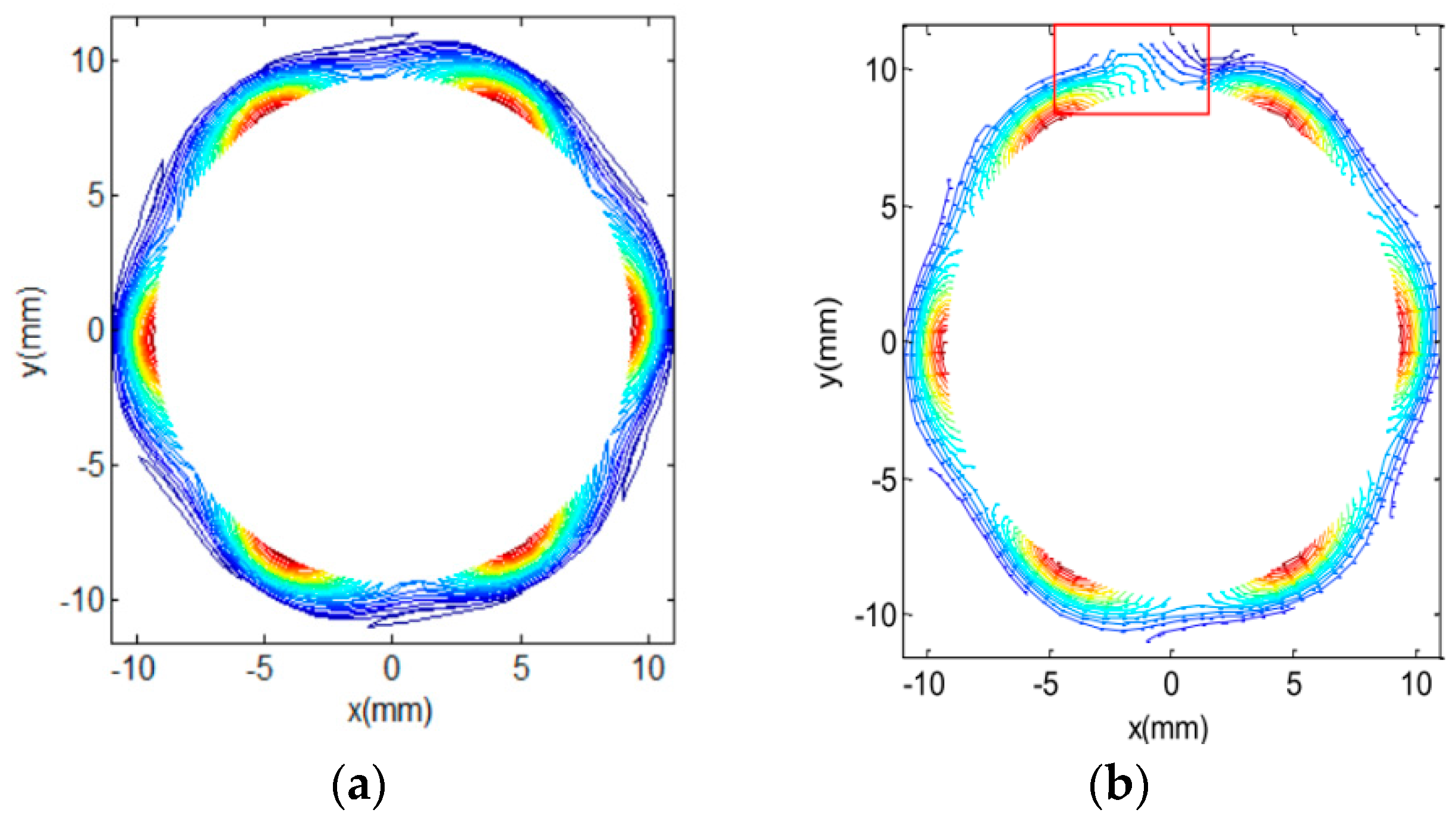
Figure 9.
Amplitude contour of magnetic field component on the xy plane: (a) defect-free; (b) defect at 90°.
Figure 9.
Amplitude contour of magnetic field component on the xy plane: (a) defect-free; (b) defect at 90°.
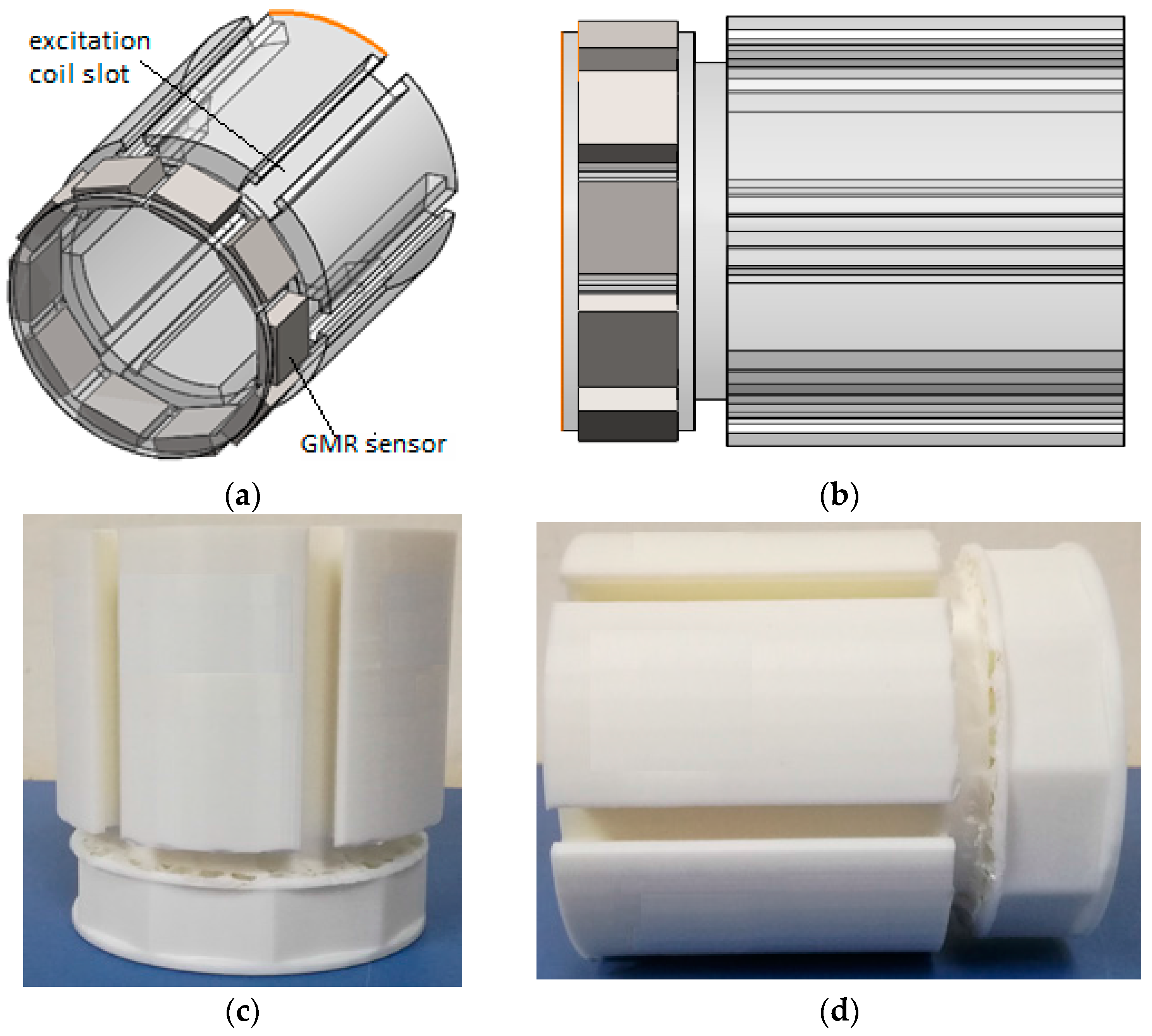
Figure 10.
Array of GMR sensor: 3-D design array of GMR sensor (a) Overall Probe (b) 3-D design of array GMR sensor inside the pipe (c) Coordinate transform from Cartesian to Cylindrical coordinate.
Figure 10.
Array of GMR sensor: 3-D design array of GMR sensor (a) Overall Probe (b) 3-D design of array GMR sensor inside the pipe (c) Coordinate transform from Cartesian to Cylindrical coordinate.
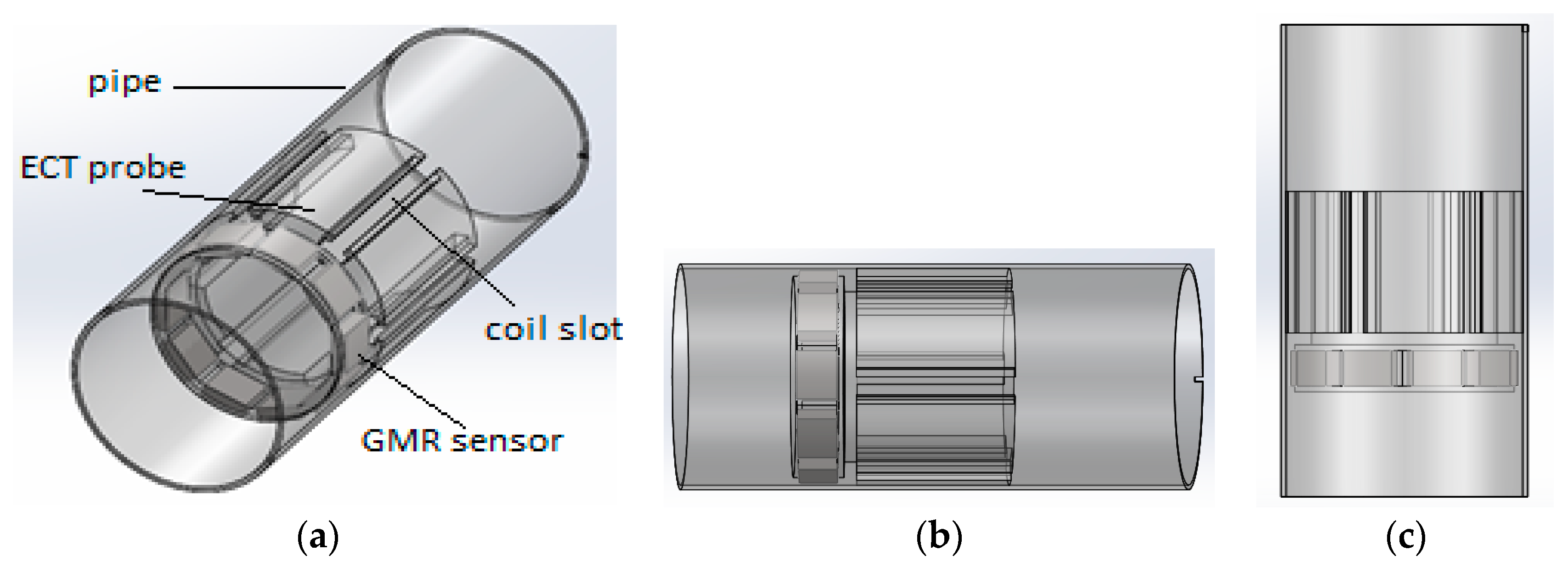
Figure 11.
Array GMR sensor located at the ECT probe for pipe inspection (a) overall probe (b) side view (c) top view.
Figure 11.
Array GMR sensor located at the ECT probe for pipe inspection (a) overall probe (b) side view (c) top view.
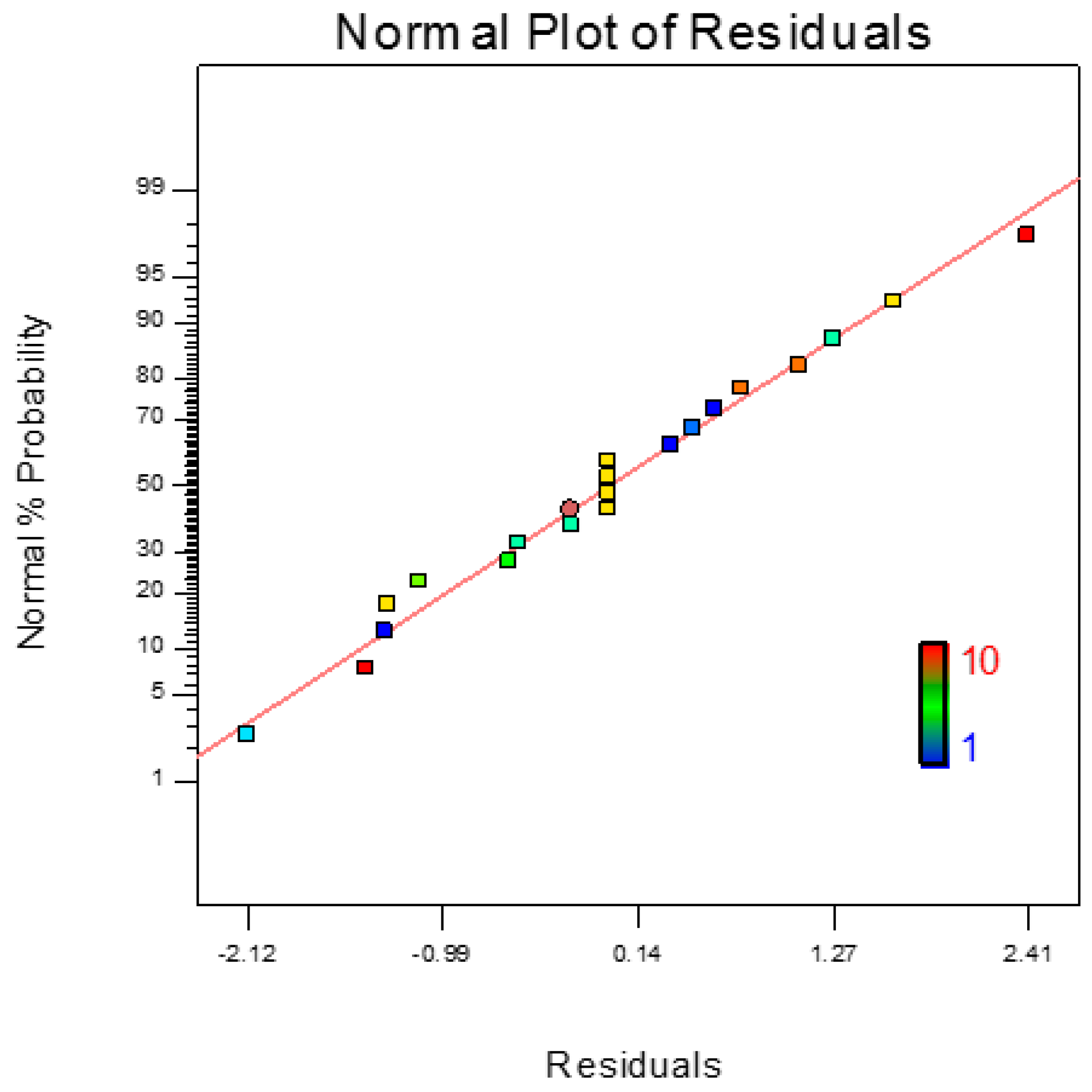
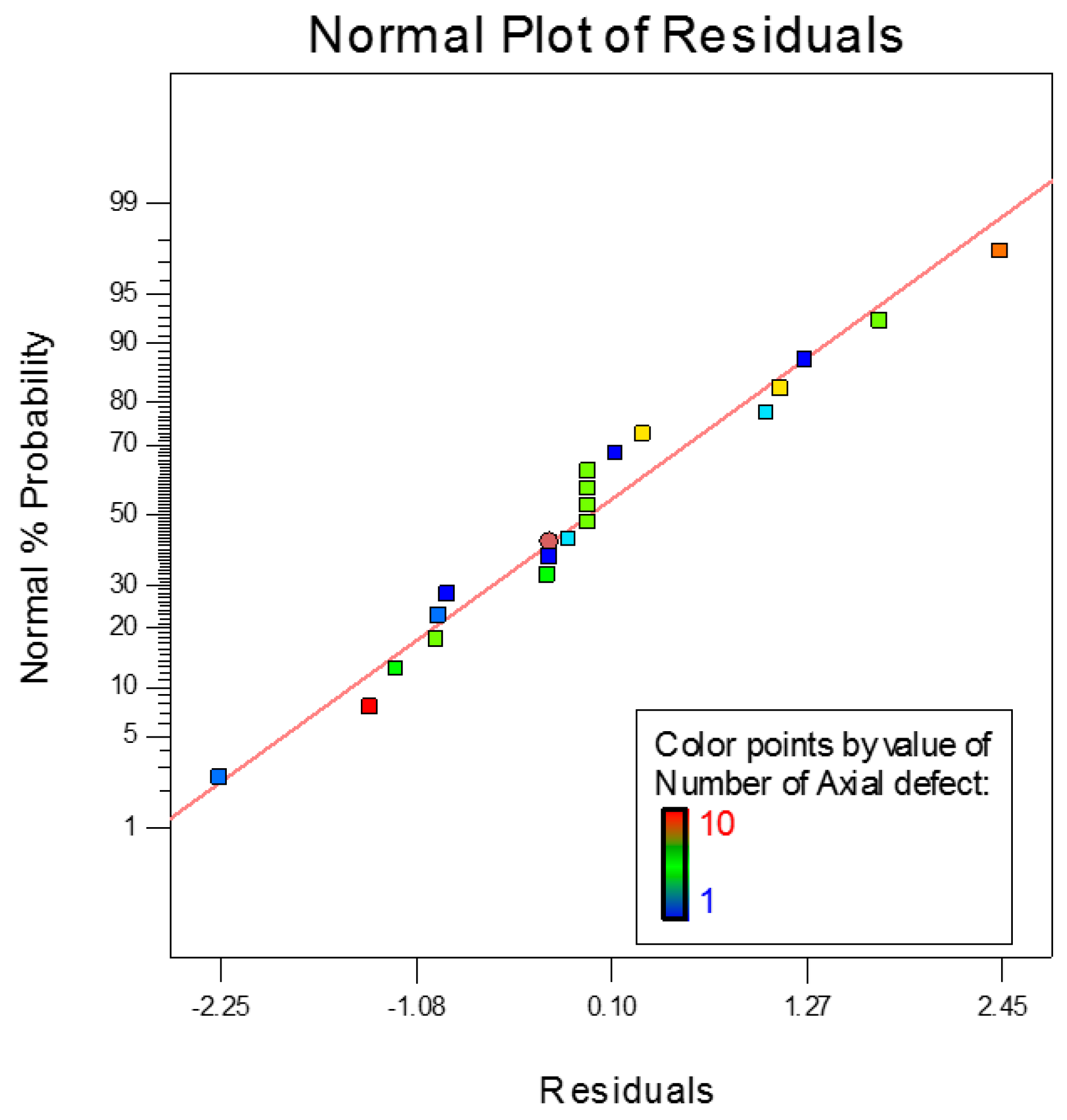
Figure 12.
Normal probability plot for axial defect detection.
Figure 12.
Normal probability plot for axial defect detection.
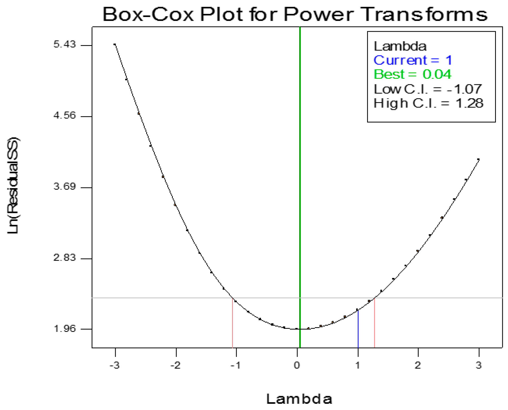
Figure 13.
Axial defect detection Box-Cox Plot for power transforms.
Figure 13.
Axial defect detection Box-Cox Plot for power transforms.
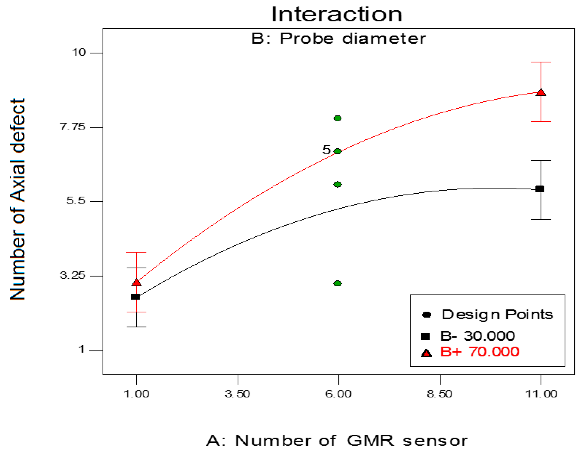
Figure 14.
Interaction of probe design factors between probe diameter and the number of GMR sensor on axial defect detection (coil thickness = 12.00 mm).
Figure 14.
Interaction of probe design factors between probe diameter and the number of GMR sensor on axial defect detection (coil thickness = 12.00 mm).
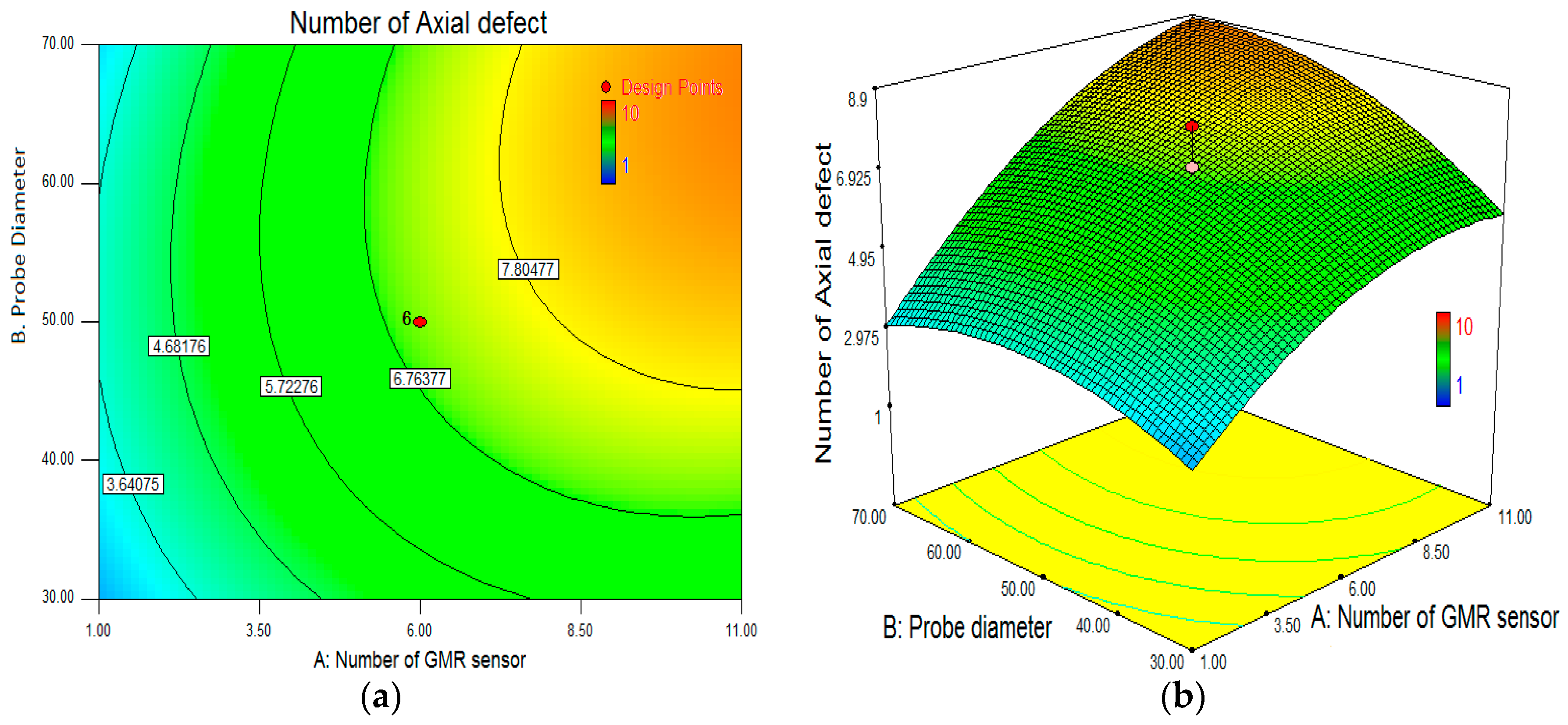
Figure 15.
Influence of number GMR sensor and ECT probe diameter in axial defect detection. (a) Contour plot; (b) 3D surface plot.
Figure 15.
Influence of number GMR sensor and ECT probe diameter in axial defect detection. (a) Contour plot; (b) 3D surface plot.
Figure 16.
Normal probability plot for circumferential defect detection.
Figure 16.
Normal probability plot for circumferential defect detection.
Figure 17.
Interaction of probe design factors between probe diameter and the number of GMR sensor on circumference defect detection (coil thickness = 31.00 mm).
Figure 17.
Interaction of probe design factors between probe diameter and the number of GMR sensor on circumference defect detection (coil thickness = 31.00 mm).
Figure 18.
Influence of number GMR sensor and ECT probe diameter in circumferential defect detection. (a) Contour plot; (b) 3D surface plot.
Figure 18.
Influence of number GMR sensor and ECT probe diameter in circumferential defect detection. (a) Contour plot; (b) 3D surface plot.
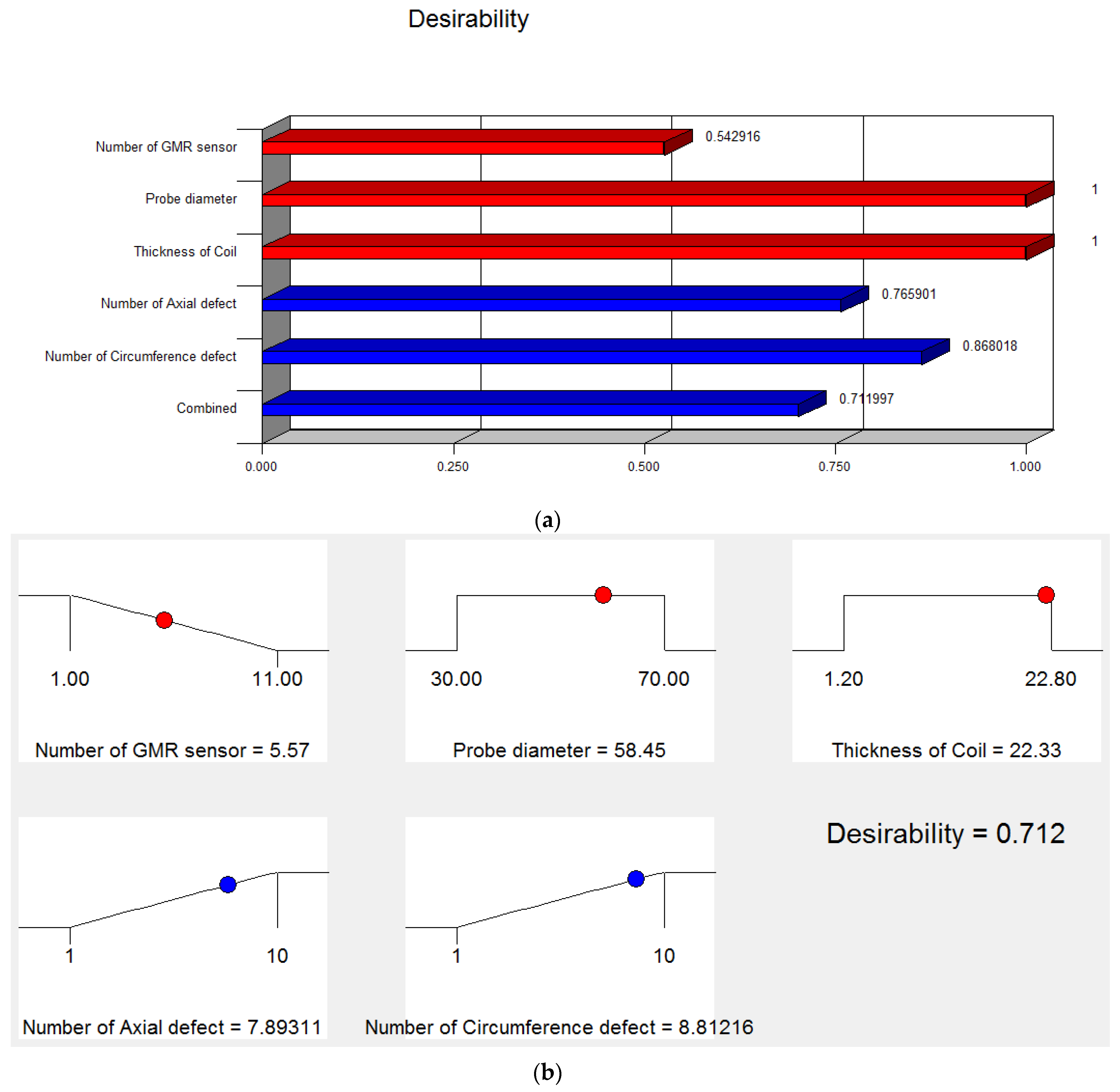
Figure 19.
Optimization solution for ECT probe design (a) Desirability graph (b) Ramp function graph.
Figure 19.
Optimization solution for ECT probe design (a) Desirability graph (b) Ramp function graph.
Figure 20.
Prediction of defect detection under optimum ECT probe design. (a,b) shows the contour graph for axial and circumference defect detection; (c,d) show the and 3-D graph for the axial and circumference defect detection.
Figure 20.
Prediction of defect detection under optimum ECT probe design. (a,b) shows the contour graph for axial and circumference defect detection; (c,d) show the and 3-D graph for the axial and circumference defect detection.
Figure 21.
ECT probe design for DSECT system based on optimum parameter design (a) Trimetric view (b) Left view (c) Probe prototype (d) Probe with GMR sensor.
Figure 21.
ECT probe design for DSECT system based on optimum parameter design (a) Trimetric view (b) Left view (c) Probe prototype (d) Probe with GMR sensor.
Figure 22.
Axial magnetic flux density due to different defect with 100% depth measure by GMR sensors: axial defect (a) 2D; (b) 3D, circumferential defect (c) 2D; (d) 3D.
Figure 22.
Axial magnetic flux density due to different defect with 100% depth measure by GMR sensors: axial defect (a) 2D; (b) 3D, circumferential defect (c) 2D; (d) 3D.
Figure 23.
Geometric dimensions of the circumference defects on the carbon steel pipe.
Figure 23.
Geometric dimensions of the circumference defects on the carbon steel pipe.
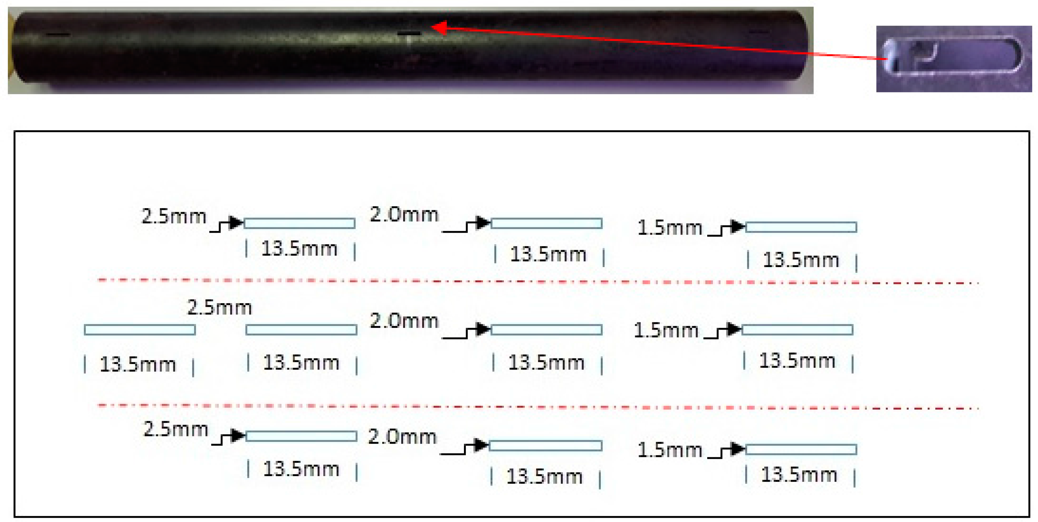
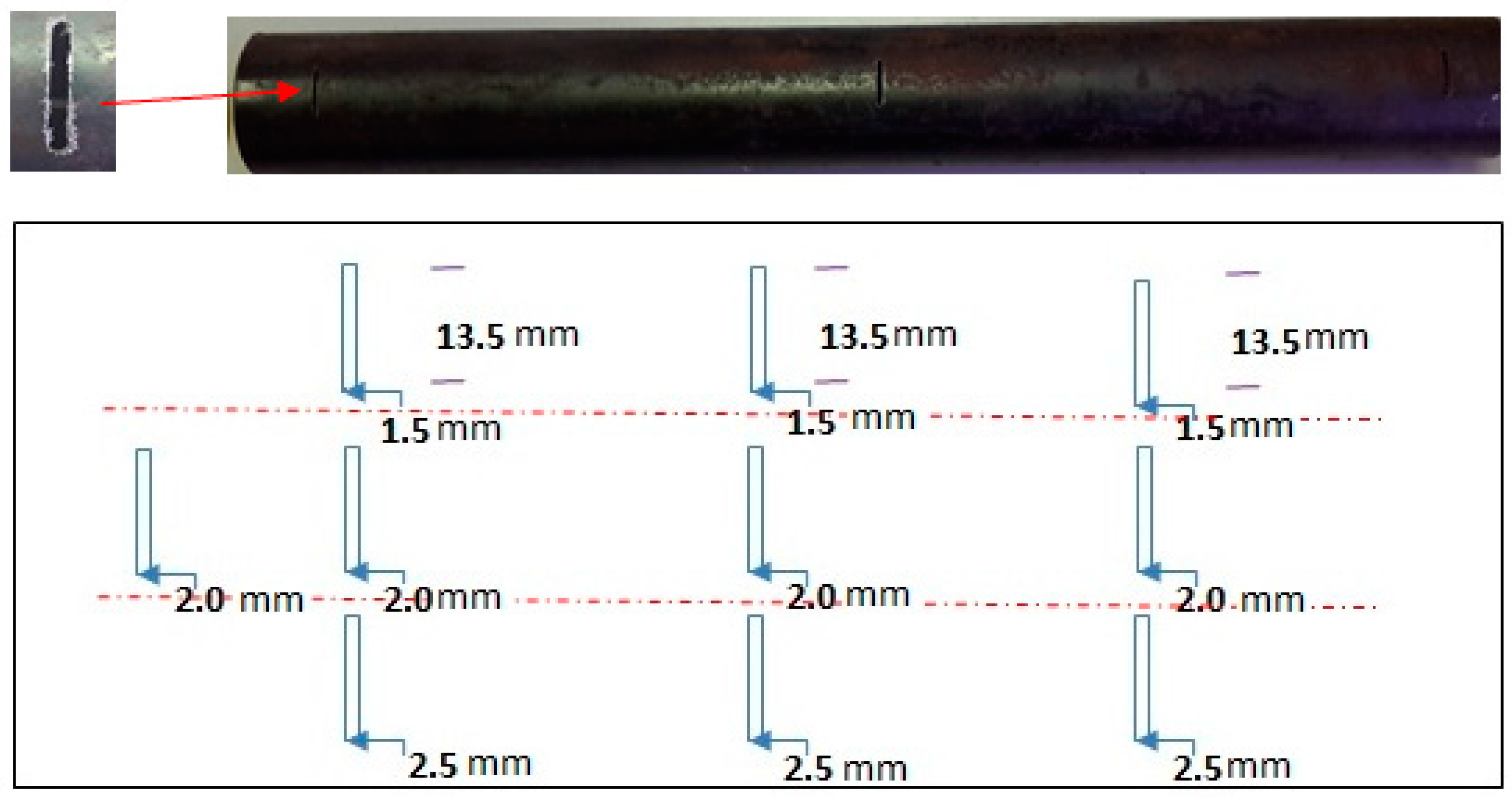
Figure 24.
Geometric dimensions of the axial defects on the carbon steel pipe.
Figure 24.
Geometric dimensions of the axial defects on the carbon steel pipe.
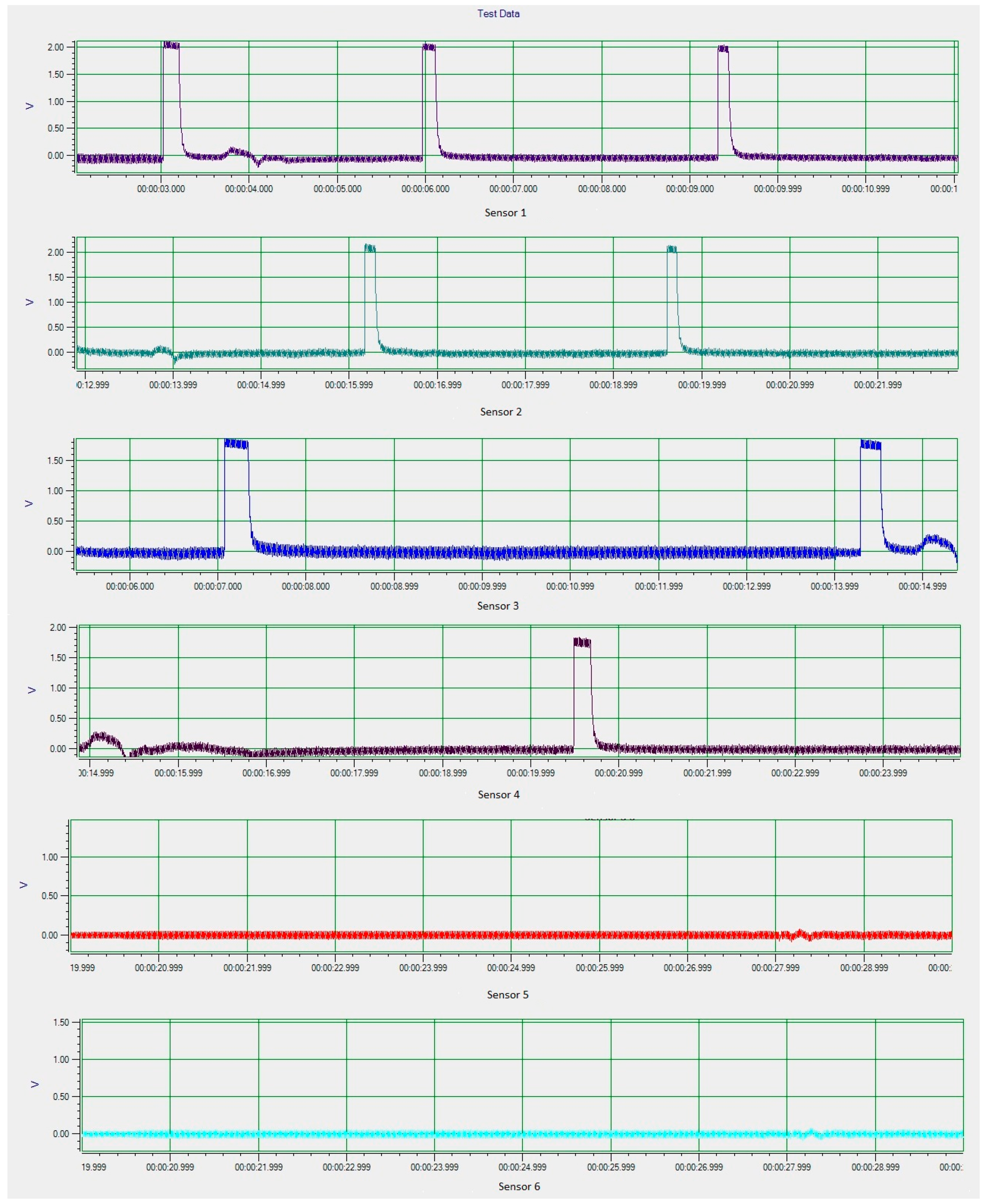
Figure 25.
Experimental results for circumference defects.
Figure 25.
Experimental results for circumference defects.
Figure 26.
Experimental result for axial defects.
Figure 26.
Experimental result for axial defects.
Table 1.
Target value and limit for optimization of DSCET probe design.
Table 1.
Target value and limit for optimization of DSCET probe design.
| Probe Design Parameter and Respond | Target | Lower Limit | Upper Limit |
|---|
| Number of GMR sensor | Minimize | 1 | 11 |
| Probe diameter (mm) | Minimize | 30 | 70 |
| Coil thickness (mm) | Minimize | 1.2 | 22.8 |
| Axial defect | Maximize | 1 | 10 |
| Circumference defect | Maximize | 1 | 10 |
Table 2.
Experimental design and results (uncoded factors).
Table 2.
Experimental design and results (uncoded factors).
| Run | Factor 1 A: Number GMR Sensor | Factor 2 B: Probe Diameter (mm) | Factor 3 C: Thickness of Coil (mm) | Response 1 Axial Defect Detect | Response 2 Circumference Defect Detect |
|---|
| 1 | 6.00 | 50.00 | 6.16 | 1 | 1 |
| 2 | 6.00 | 50.00 | 12.00 | 7 | 8 |
| 3 | 11.00 | 30.00 | 1.20 | 3 | 4 |
| 4 | 6.00 | 50.00 | 12.00 | 7 | 8 |
| 5 | 1.00 | 30.00 | 1.20 | 1 | 1 |
| 6 | 1.00 | 70.00 | 1.20 | 1 | 2 |
| 7 | 11.00 | 30.00 | 22.80 | 7 | 8 |
| 8 | 6.00 | 16.36 | 12.00 | 3 | 4 |
| 9 | 2.41 | 50.00 | 12.00 | 1 | 1 |
| 10 | 11.00 | 70.00 | 1.20 | 5 | 6 |
| 11 | 6.00 | 50.00 | 30.16 | 9 | 10 |
| 12 | 1.00 | 70.00 | 22.80 | 2 | 3 |
| 13 | 1.00 | 30.00 | 22.80 | 2 | 4 |
| 14 | 6.00 | 83.64 | 12.00 | 7 | 8 |
| 15 | 6.00 | 50.00 | 12.00 | 6 | 7 |
| 16 | 6.00 | 50.00 | 12.00 | 8 | 9 |
| 17 | 6.00 | 50.00 | 12.00 | 7 | 8 |
| 18 | 6.00 | 50.00 | 12.00 | 7 | 8 |
| 19 | 14.41 | 50.00 | 12.00 | 8 | 9 |
| 20 | 11.00 | 70.00 | 22.80 | 10 | 10 |
Table 3.
ANOVA table for axial defect detection response surface quadratic model.
Table 3.
ANOVA table for axial defect detection response surface quadratic model.
| Source | Sum of Squares | df | Mean Square | F Value | p-Value Prob> F Prob > F | Remarks |
|---|
| Model | 164.81 | 9 | 18.31 | 20.38 | <0.0001 | significant |
| A-Nu sensor | 69.34 | 1 | 69.34 | 77.16 | <0.0001 | significant |
| B-diameter | 10.07 | 1 | 10.07 | 11.21 | 0.0074 | significant |
| C-coil thickness | 43.79 | 1 | 43.79 | 48.73 | <0.0001 | significant |
| AC | 6.13 | 1 | 6.13 | 6.82 | 0.0260 | significant |
| A2 | 16.14 | 1 | 16.14 | 17.96 | 0.0017 | significant |
| B2 | 11.20 | 1 | 11.20 | 12.46 | 0.0054 | significant |
| C2 | 11.20 | 1 | 11.20 | 12.46 | 0.0054 | significant |
| Residual | 8.99 | 10 | 0.90 | | | |
| Lack of Fit | 6.99 | 5 | 1.40 | 3.49 | 0.0980 | not significant |
| Pure Error | 2.00 | 5 | 0.40 | | | |
| Cor Total | 173.80 | 19 | | | | |
Table 4.
ANOVA for the circumference defect detection response surface quadratic model.
Table 4.
ANOVA for the circumference defect detection response surface quadratic model.
| Source | Sum of Squares | df | Mean Square | F Value | p-Value Prob > F Prob > F | Remarks |
|---|
| Model | 177.10 | 9 | 19.68 | 19.97 | <0.0001 | significant |
| A-Nu sensor | 72.45 | 1 | 72.45 | 73.53 | <0.0001 | significant |
| B-diameter | 8.43 | 1 | 8.43 | 8.55 | 0.0152 | significant |
| C-coil thickness | 53.92 | 1 | 53.92 | 54.73 | <0.0001 | significant |
| A2 | 20.30 | 1 | 20.30 | 20.61 | 0.0011 | significant |
| B2 | 10.01 | 1 | 10.01 | 10.16 | 0.0097 | significant |
| C2 | 14.71 | 1 | 14.71 | 14.93 | 0.0031 | significant |
| Residual | 9.85 | 10 | 0.99 | | | significant |
| Lack of Fit | 7.85 | 5 | 1.57 | 3.93 | 0.0798 | not significant significant |
| Pure Error | 2.00 | 5 | 0.40 | | | |
| Cor Total | 186.95 | 19 | | | | |
Table 5.
Simulation defect parameters.
Table 5.
Simulation defect parameters.
| Type of Defect | Dimension |
|---|
| Width (mm) | Length (mm) | Depth (mm) |
|---|
| Axial | 12 | 2 | 5 |
| Circumference | 2 | 12 | 5 |
Table 6.
Comparison of the predicted and experimental results.
Table 6.
Comparison of the predicted and experimental results.
| Defect | Prediction | Experimental | Error (%) |
|---|
| Axial | 7.89535 | 8 | −1.32 |
| Circumference | 8.8141 | 9 | −2.11 |


