
A Low-G Silicon Inertial Micro-Switch with Enhanced Contact Effect Using Squeeze-Film Damping


Abstract
:1. Introduction
2. Design and FEM Simulation
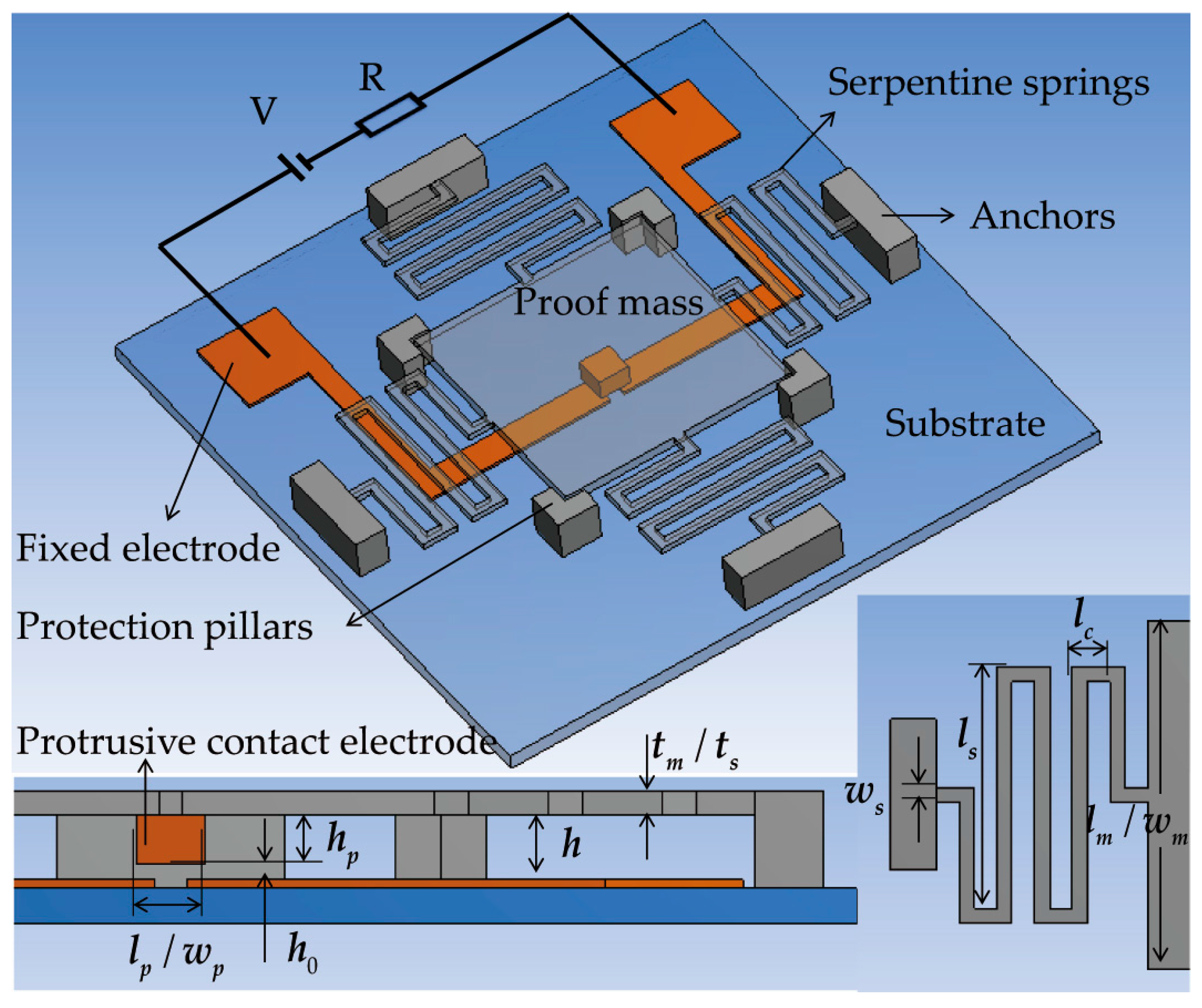
2.1. Device Design
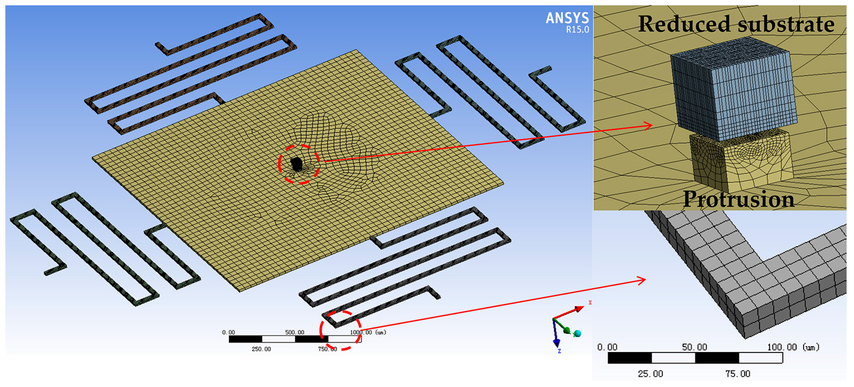
2.2. FEM Simulation
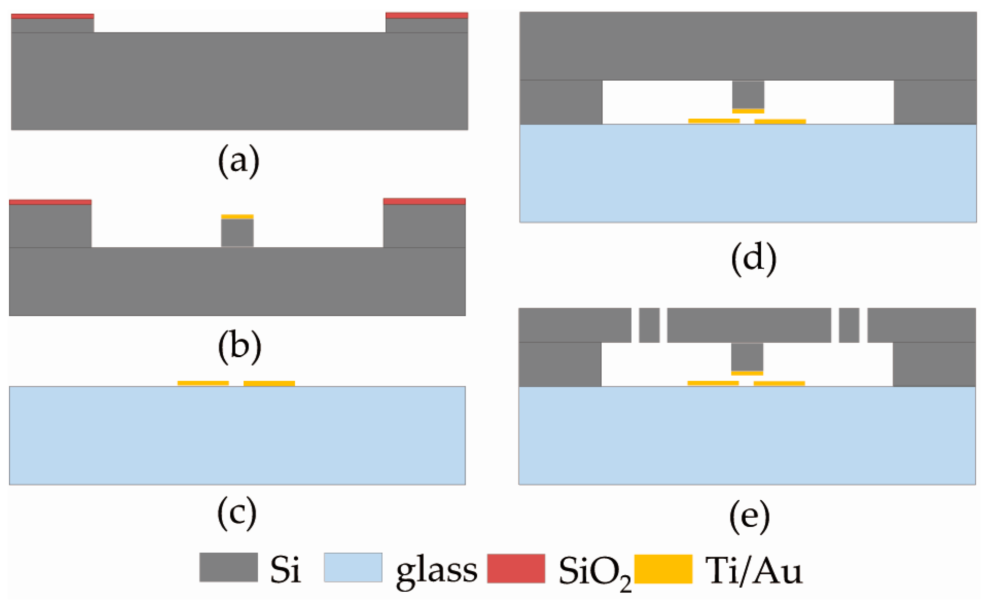
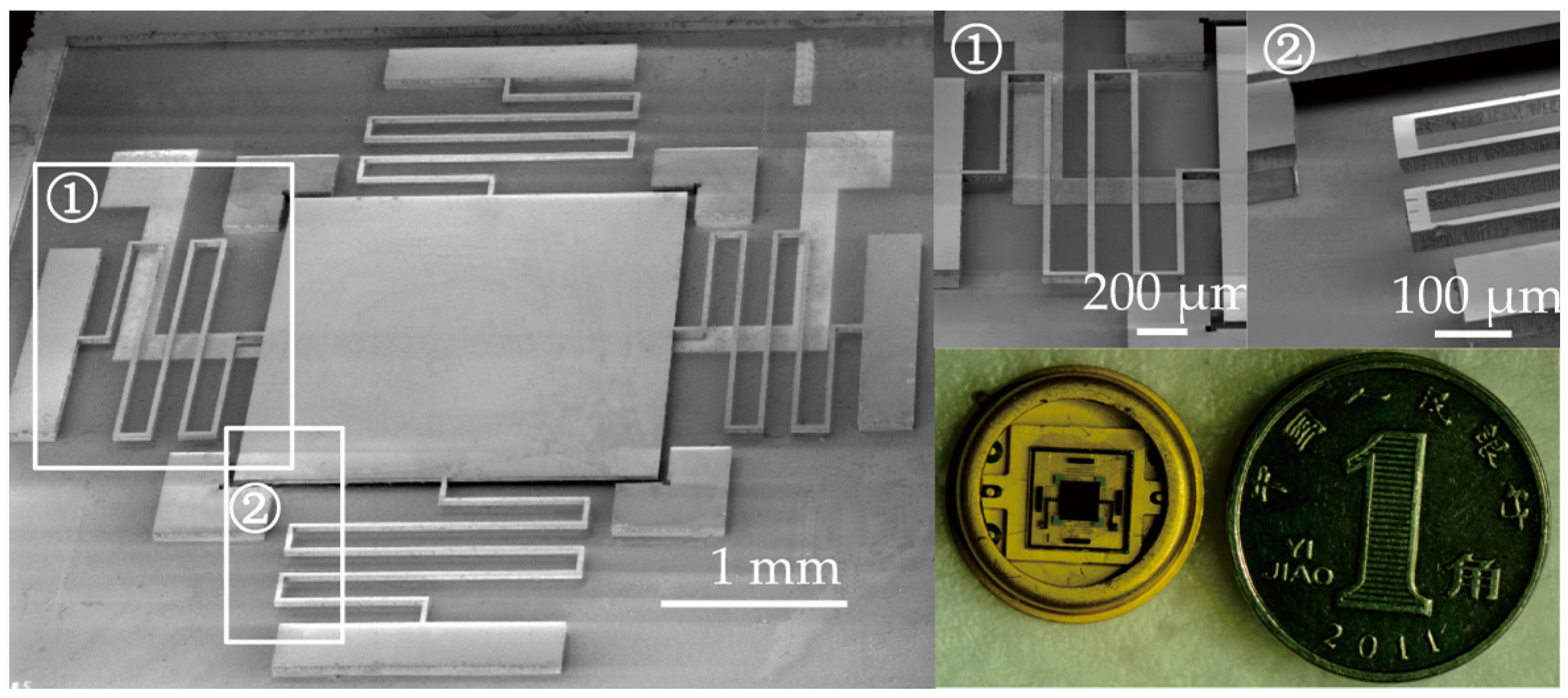
3. Fabrication
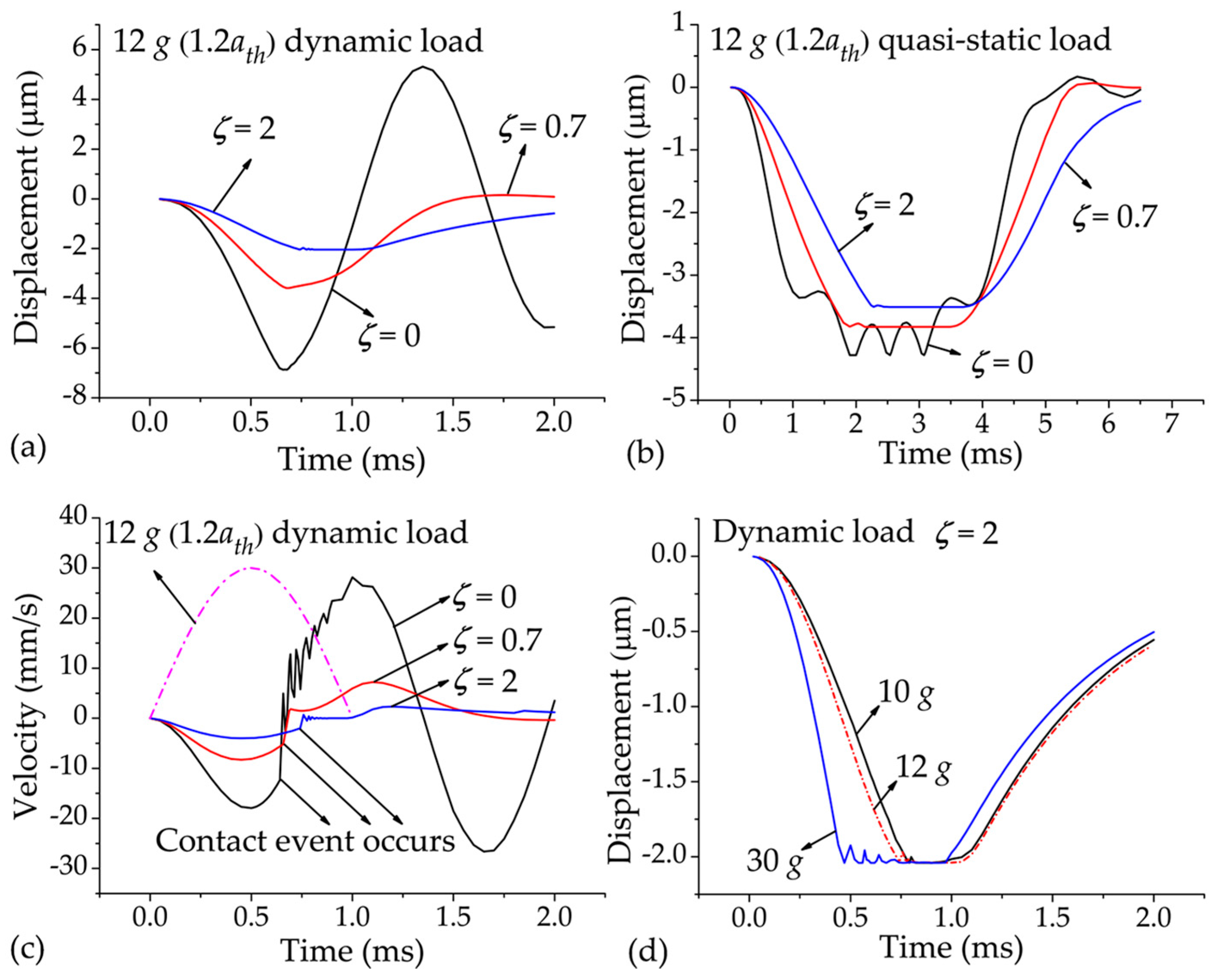
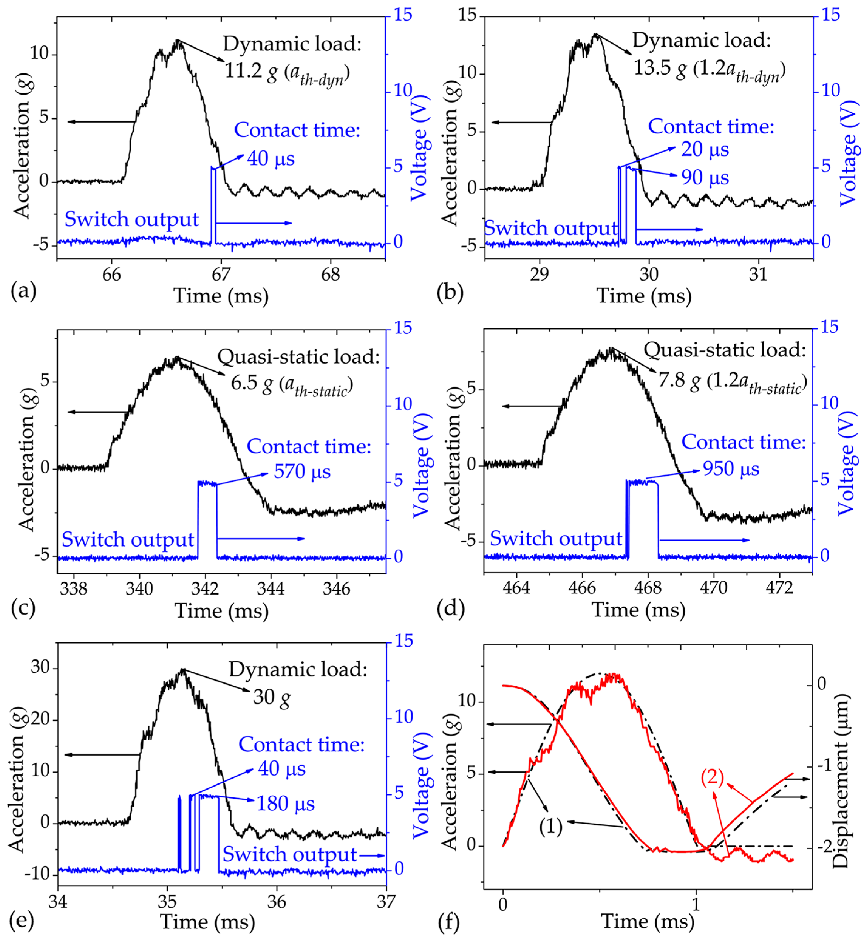
4. Results and Discussion
5. Conclusions
Acknowledgments
Author Contributions
Conflicts of Interest
References
- Ongkodjojo, A.; Tay, F.E.H. Optimized design of a micromachined G-switch based on contactless configuration for health care applications. J. Phys. Conf. Ser. 2006, 34, 1044–1052. [Google Scholar] [CrossRef]
- Wang, Y.; Feng, Q.; Wang, Y.; Chen, W.; Wang, Z.; Ding, G.; Zhao, X. The design, simulation and fabrication of a novel horizontal sensitive inertial micro-switch with low g value based on MEMS micromachining technology. J. Micromech. Microeng. 2013, 23, 105013. [Google Scholar] [CrossRef]
- Ma, W.; Li, G.; Zohar, Y.; Wong, M. Fabrication and packaging of inertia micro-switch using low-temperature photo-resist molded metal-electroplating technology. Sens. Actuators A Phys. 2004, 111, 63–70. [Google Scholar] [CrossRef]
- Currano, L.J.; Becker, C.R.; Lunking, D.; Smith, G.L.; Thomas, L. Triaxial inertial switch with multiple thresholds and resistive ladder readout. Sens. Actuators A Phys. 2013, 195, 191–197. [Google Scholar] [CrossRef]
- Frobenius, W.D.; Zeitman, S.A.; White, M.H.; O’Sullivan, D.D. Microminiature ganged threshold accelerometers compatible with integrated circuit technology. IEEE Trans. Electron. Dev. 1972, 19, 37–40. [Google Scholar] [CrossRef]
- Currano, L.J.; Yu, M.; Balachandran, B. Latching in a MEMS shock sensor: Modeling and experiments. Sens. Actuators A Phys. 2010, 159, 41–50. [Google Scholar] [CrossRef]
- Lee, Y.; Sim, S.M.; Kim, H.; Kim, Y.K.; Kim, J.M. Silicon MEMS acceleration switch with high reliability using hooked latch. Microelectron. Eng. 2016, 152, 10–19. [Google Scholar] [CrossRef]
- Dellaert, D.; Doutreloigne, J. A thermally-actuated latching MEMS switch matrix and driver chip for an automated distribution frame. Mechatronics 2016, 40, 287–292. [Google Scholar] [CrossRef]
- Frangi, A.; de Masi, B.; Confalonieri, F.; Baldasarre, L. Threshold shock sensor based on a bi-stable mechanism. J. Microelectromech. Syst. 2015, 24, 2019–2026. [Google Scholar] [CrossRef]
- Zhao, J.; Liu, P.; Tang, Z.; Fan, K. A wireless MEMS inertial switch for measuring both threshold triggering acceleration and response time. IEEE Trans. Instrum. Meas. 2014, 63, 3152–3161. [Google Scholar] [CrossRef]
- Yoo, K.; Park, U.; Kim, J. Development and characterization of a novel configurable MEMS inertial switch using a microscale liquid-metal droplet in a microstructured channel. Sens. Actuators A Phys. 2011, 166, 234–240. [Google Scholar] [CrossRef]
- Liu, T.; Wei, S.; Tao, Y.; Yuan, X. Vibration interference analysis and verification of micro-fluidic inertial switch. AIP Adv. 2014, 4, 32–33. [Google Scholar]
- Gerson, Y.; Schreiber, D.; Grau, H.; Krylov, S. Meso scale MEMS inertial switch fabricated using an electroplated metal-on-insulator process. J. Micromech. Microeng. 2014, 24, 405–412. [Google Scholar] [CrossRef]
- Xi, Z.; Ping, Z.; Nie, W.; Du, L.; Yun, C. A novel MEMS omnidirectional inertial switch with flexible electrodes. Sens. Actuators A Phys. 2014, 212, 93–101. [Google Scholar]
- Yang, Z.; Cai, H.; Ding, G.; Wang, H.; Zhao, X. Dynamic simulation of a contact-enhanced MEMS inertial switch in Simulink. Microsyst. Technol. 2011, 17, 1329–1342. [Google Scholar] [CrossRef]
- Yang, Z.; Ding, G.; Cai, H.; Xu, X.; Wang, H.; Zhao, X. Analysis and elimination of the ‘skip contact’ phenomenon in an inertial micro-switch for prolonging its contact time. J. Micromech. Microeng. 2009, 19, 045017. [Google Scholar] [CrossRef]
- Chen, W.; Wang, Y.; Wang, Y.; Zhu, B.; Ding, G.; Wang, H.; Zhao, X.; Yang, Z. A laterally-driven micromachined inertial switch with a compliant cantilever beam as the stationary electrode for prolonging contact time. J. Micromech. Microeng. 2014, 24, 65020–65029. [Google Scholar] [CrossRef]
- Zhang, Q.; Xu, Q.; Wang, Y.; Ding, G.; Zhao, X.; Yang, Z. Design and fabrication of a laterally-driven inertial micro-switch with multi-directional constraint structures for lowering off-axis sensitivity. J. Micromech. Microeng. 2016, 26, 055008. [Google Scholar] [CrossRef]
- Xu, Q.; Yang, Z.; Fu, B.; Li, J.; Wu, H.; Zhang, Q.; Sun, Y.; Ding, G.; Zhao, X. A surface-micromachining-based inertial micro-switch with compliant cantilever beam as movable electrode for enduring high shock and prolonging contact time. Appl. Surf. Sci. 2016, 387, 569–580. [Google Scholar] [CrossRef]
- Wycisk, M.; Tonnesen, T.; Binder, J.; Michaelis, S.; Timme, H.J. Low-cost post-CMOS integration of electroplated microstructures for inertial sensing. Sens. Actuators A Phys. 2000, 83, 93–100. [Google Scholar] [CrossRef]
- Bao, M. Analysis and Design Principles of MEMS Devices; Elsevier: Amsterdam, The Netherlands, 2005; pp. 128–161. [Google Scholar]
- Pantano, M.F.; Pagnotta, L.; Nigro, S. A numerical study of squeeze-film damping in MEMS-based structures including rarefaction effects. Frat. Integr. Strutt. 2013, 23, 103–113. [Google Scholar]
- Bao, M.; Yang, H. Squeeze film air damping in MEMS. Sens. Actuators A Phys. 2007, 136, 3–27. [Google Scholar] [CrossRef]
- Hsia, Y.T.; Domoto, G.A. An experimental investigation of molecular rarefaction effects in gas lubricated bearings at ultra-low clearances. J. Tribol. 1981, 105, 120–130. [Google Scholar] [CrossRef]
- Sadd, M.H.; Stiffler, A.K. Squeeze film dampers: Amplitude effects at low squeeze numbers. J. Eng. Ind. 1975, 4, 1366–1370. [Google Scholar] [CrossRef]
- Veijola, T.; Kuisma, H.; Lahdenperä, J.; Ryhänen, T. Equivalent-circuit model of the squeezed gas film in a silicon accelerometer. Sens. Actuators A Phys. 1995, 48, 239–248. [Google Scholar] [CrossRef]
- Liu, M.; Gorman, D.G. Formulation of Rayleigh damping and its extensions. Comput. Struct. 1995, 57, 277–285. [Google Scholar] [CrossRef]


| 2300 | 50 | 20 | 1600 | 150 | 30 | Variable | Variable |
| Material | Density | Young’s Modulus | Poisson’s Ratio |
|---|---|---|---|
| Silicon | 2330 kg/m3 | 169 GPa | 0.28 |
| Glass | 2200 kg/m3 | 70 GPa | 0.17 |
© 2017 by the authors. Licensee MDPI, Basel, Switzerland. This article is an open access article distributed under the terms and conditions of the Creative Commons Attribution (CC BY) license ( http://creativecommons.org/licenses/by/4.0/).
Share and Cite
Peng, Y.; Wen, Z.; Li, D.; Shang, Z. A Low-G Silicon Inertial Micro-Switch with Enhanced Contact Effect Using Squeeze-Film Damping. Sensors 2017, 17, 387. https://doi.org/10.3390/s17020387
Peng Y, Wen Z, Li D, Shang Z. A Low-G Silicon Inertial Micro-Switch with Enhanced Contact Effect Using Squeeze-Film Damping. Sensors. 2017; 17(2):387. https://doi.org/10.3390/s17020387
Chicago/Turabian StylePeng, Yingchun, Zhiyu Wen, Dongling Li, and Zhengguo Shang. 2017. "A Low-G Silicon Inertial Micro-Switch with Enhanced Contact Effect Using Squeeze-Film Damping" Sensors 17, no. 2: 387. https://doi.org/10.3390/s17020387