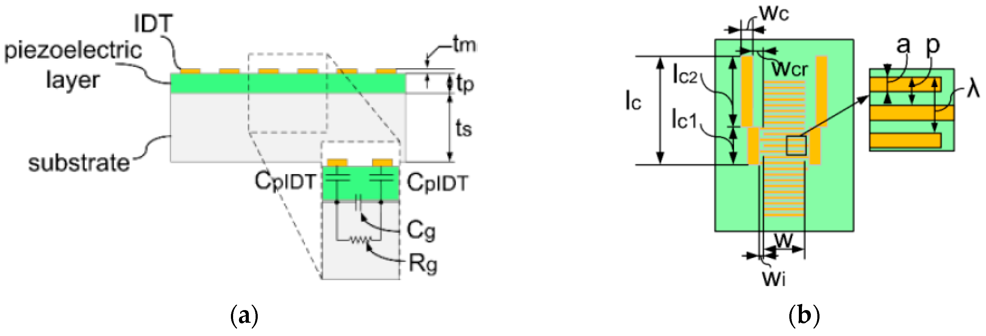
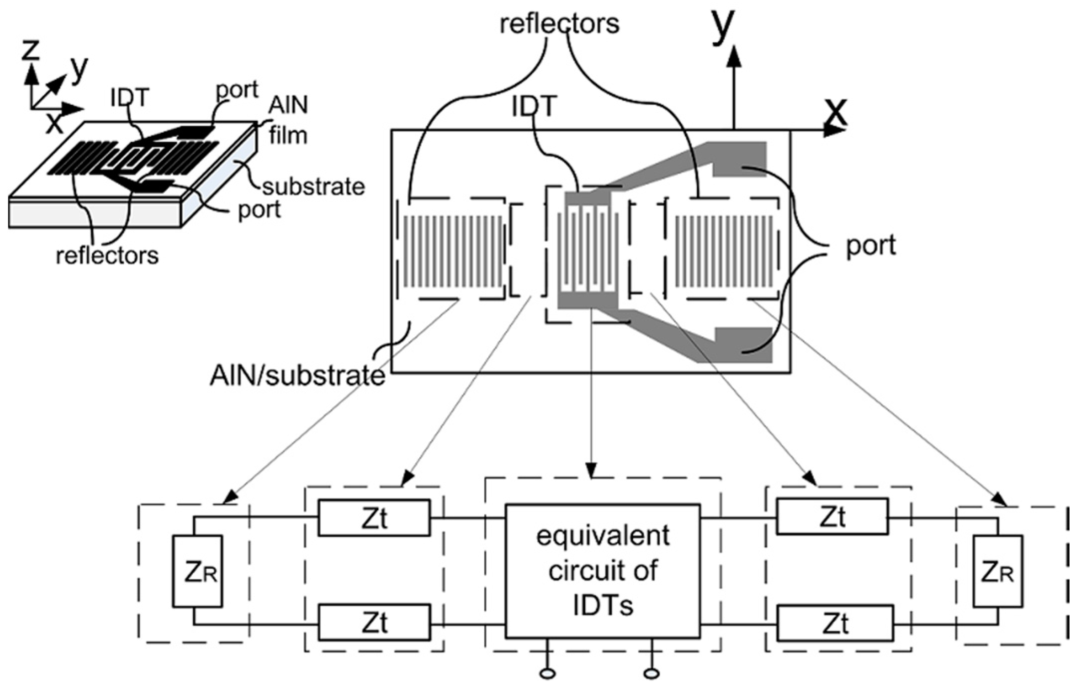
2.1. Modification of the Equivalent Circuit of IDT
With the existence of the aforementioned parasitic parameters from the semiconducting substrate, the equivalent electrical components between IDT grids are modified, as shown in
Figure 2a, where C
pIDT represents the capacitor of the piezoelectric layer under the IDT electrodes, R
g represents the resistor from the substrate at the gap between the IDT electrodes, and C
g represents the capacitor from the substrate and piezoelectric layer at the same area.
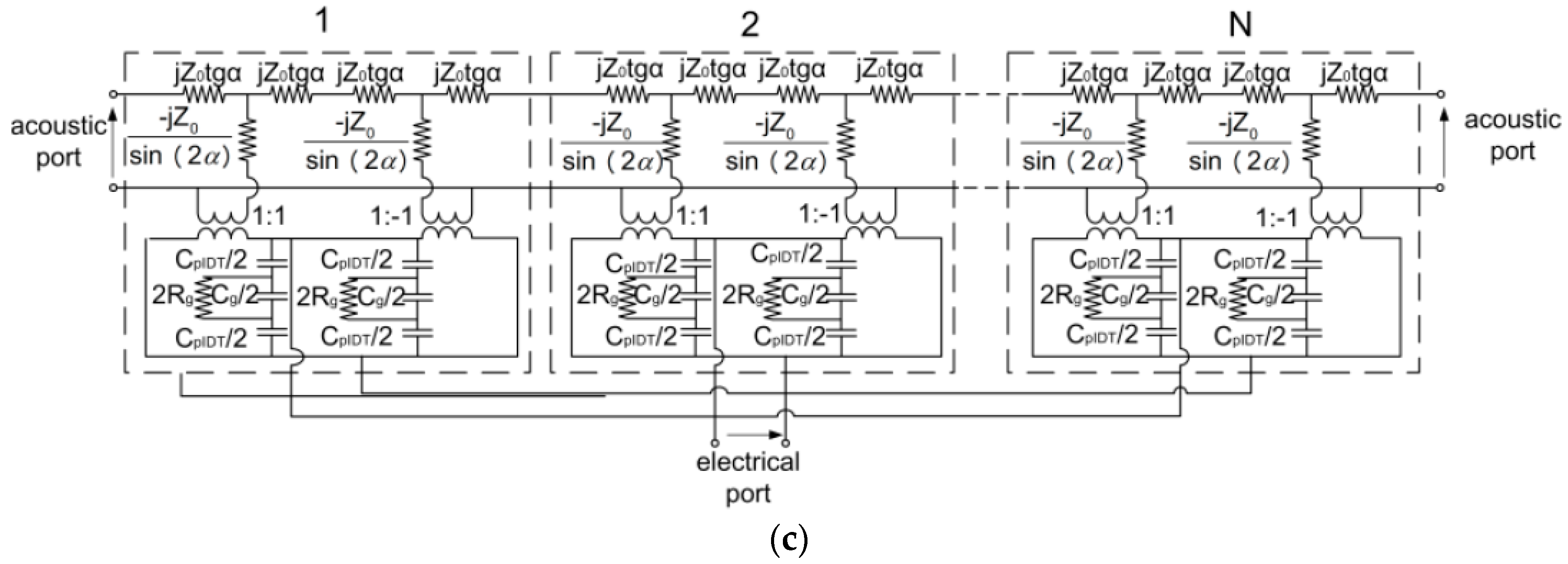
Thus the equivalent circuit model of the IDT part can be derived by combining the equivalent circuits of single pair IDT, as shown in
Figure 2c. The acoustic ports of single IDT are connected in serial and the electrical ports are connected in parallel. With the geometric definitions of the SAWR in
Figure 2b, the equivalent circuit components can be given as:
where R
□ is the square resistance of the substrate, t
p is the thickness of the piezoelectric layer, t
s is the thickness of the substrate, ε
s,c and ε
p are the complex relative permittivity of the substrate and the piezoelectric layer, respectively. Z
0 is the equivalent electrical impedance representing the acoustic impedance from the piezoelectric layer and the substrate, and has been given by [
20] as:
where ω
0 is the angular resonant frequency of SAWR, C
s is the static capacitor storing the electrical energy between the IDT electrodes, and can be given by Equation (5), where C
g,r is the real part of C
g:
K
2 is the electrical-mechanical coupling coefficient of the piezoelectric material, and can be derived experimentally through the serial and parallel resonant frequencies (f
s and f
p, respectively) of the SAWR [
21,
22]:
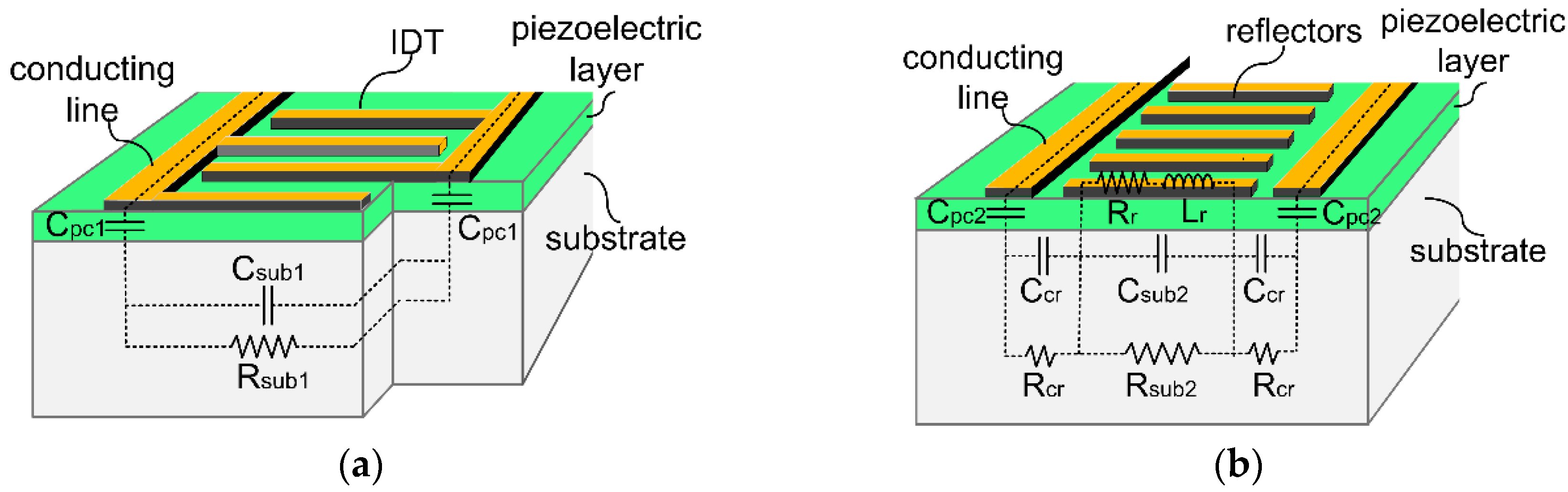
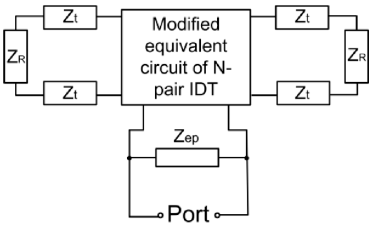
2.2. Parallel Parasitic Parameters Introduced from the Conducting Lines
The semiconducting substrate will also introduce parasitic parameters from the conducting lines which connect the IDT and the port of the stimulating signal. The equivalent circuit components of these parasitic parameters are shown in
Figure 3.
As can be seen from
Figure 3, both the IDT part (
Figure 3a) and reflector part (
Figure 3b) will introduce parasitic effects from the substrate.
In the IDT part, each components are outlined as follows: Cpc1 represents the capacitor from the piezoelectric film under the conducting lines, Csub1 represents the capacitor from the substrate between the conducting lines, and Rsub1 represents the resistor from the substrate at the same region.
In the reflector part, Cpc2 represents the same as defined in the IDT part; Rr represents the resistor of the reflecting grids; Rsub2 and Rcr represent the resistors from the substrate lying under and outside the reflector region, respectively; Csub2 and Ccr represent the capacitor from the substrate at the same aforementioned area, respectively; Lr and Rr represents the inductance and resistance from the reflecting grids, respectively.
For these aforementioned parallel parasitic parameters, the analytical formulas can be approximately given as below, among which, L
r is calculated based on the inductance of a flat conductor [
23,
24]:
They can be equivalently expressed as an impedance, namely Z
ep, which is connected in parallel with the SAWR. Z
ep can be expressed as:
2.4. Temperature Response of Electrical Performance Based on the Modified Equivalent Circuit Model
Temperature will affect the performance of SAWR devices in a complex way due to its coupling with various material properties. These temperature-coupled material properties can be categorized into functioning parameters (such as the electrical-mechanical coupling coefficients), electrical parameters (such the resistivity, relative permittivity) and mechanical parameters (such as elastic constants, mass density). Here in this section, the temperature influence on the SAWR from the aspect of substrate will be analyzed based on the modified equivalent circuit model introduced above.
As can be seen from
Section 2.1 and
Section 2.2, the parasitic parameters introduced by the semiconducting substrate are related to the square resistance R
□, the complex relative permittivity ε
s,c, and the geometric parameters, among which, R
□ can further be calculated through the resistivity (
) and the thickness of the substrate (
) as:
Therefore the parasitic parameters influenced by the temperature can further be expressed as functions of , εs,c,T, and aT, being the temperature-dependent resistivity of substrate, temperature-dependent complex relative permittivity of substrate, thermal expansion coefficient, respectively. aT is introduced here due to the variation of geometric parameters from thermal expansion.
For n-type semiconductors discussed here,
can further be expressed as [
25]:
where
and
are, respectively, the carrier mobility and electron concentration, both being temperature dependent, while e is the elementary charge and not sensitive to temperature. For a dopant concentration
lower than
,
can further be expressed as [
25]:
where
is the carrier mobility of the substrate under 300 K, and T is the absolute temperature in K. The temperature dependent electron concentration
can be expressed as [
25]:
where
is the intrinsic concentration of electrons, and can further be expressed as [
25]:
where
is the band gap of the substrate, and k is the Boltzmann constant.
and
are, respectively, the effective density of states for the conduction band and valence band, and can be expressed as [
25]:
where
and
are the effective density of states coefficients for the conduction band and valence band. The temperature dependent resistivity
can thus be given as Equation (25) by combining Equations (19)–(24).
The complex relative permittivity ε
s,c,T can be expressed by its real part
and imaginary part
as [
26]:
while the real part of
is the dielectric constant (ε
s,R) of the substrate, the imaginary part, being temperature dependent, can be expressed as Equation (27) without considering the electronic and ionic polarization [
26], where
is the dielectric constant of vacuum.
As can be seen from Equation (27), is a function of and frequency f, where has been given by Equation (25).
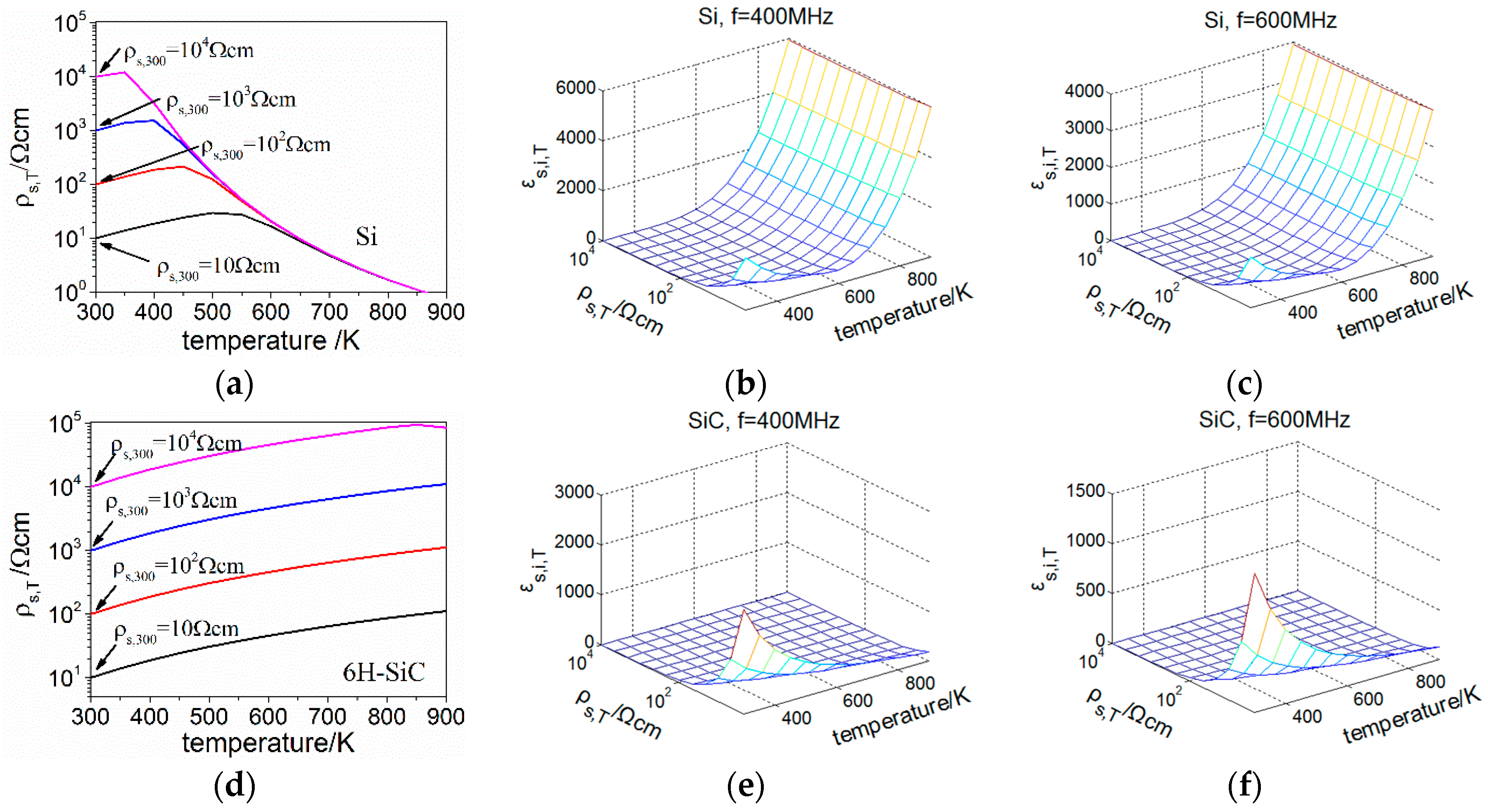
Based on the expressions listed above, the temperature response of substrate’s properties can be calculated. The chosen materials of the substrates are Si and 6H-SiC, with the nominal resistivity at 300 K (
) varying from 10 Ωcm to 10
4 Ωcm. The material parameters used in calculation are listed in
Table 1.
The intrinsic concentrations of electrons at 300 K (
) are firstly calculated by Equation (22), and the dopant concentrations (
) can further be calculated by combing Equations (19)–(21) as:
The calculated
with different
are listed in
Table 2.
Through Equations (25) and (27), the calculated
and
with different
and temperatures (300–900 K) are shown in
Figure 5.
As shown in
Figure 5a,
of Si increases slightly and then decreases as the temperature rises, indicating a collaborative effect from the decreasing carrier mobility and increasing electron concentration. At temperatures higher than 600 K, the Si substrate is highly intrinsic, and
with different
become converged. Besides, both of the calculated
of Si at 400 MHz and 600 MHz are showing an increase on orders of magnitude at temperature higher than 600 K, mainly due to the decreasing
. As can be seen from
Figure 5d,
of 6H-SiC with different
increases through the temperature range of calculation, and shows no convergence of the curves. As for
of 6H-SiC, it doesn’t manifest the increase at elevated temperatures observed in the case of Si. The different behaviors between Si and 6H-SiC are contributed to their different band gaps. 6H-SiC, with a wide band gap, shows less diversification of its electrical properties within the calculated temperature range.
Referring to Equations (1), (2), (8), (9) and (11)–(14), it can be seen that the geometric parameters are on the same order with
or ε
s,c,T, and considering that Si’s and 6H-SiC’s coefficients of thermal expansion range from around 2 ppm/C to 5 ppm/C in the temperature range of 300 to 900 K [
28,
29], which is much lower than the relative changes of
or ε
s,c,T, the effect from thermal expansion can be neglected.
With the calculated
and
, the temperature performance of SAWR can thus be derived through the modified equivalent circuit model introduced in this work. The geometric parameters and material properties used in the calculation are listed in
Table A1 of
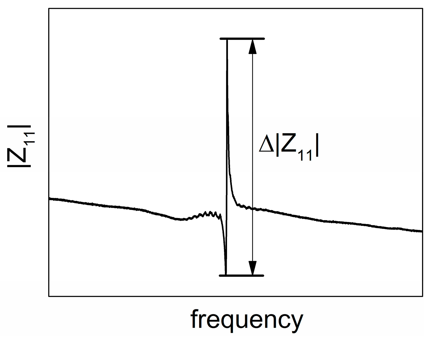
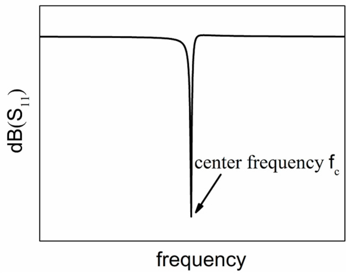
Appendix A. And molybdenum (Mo) is chosen as the metal material for IDT and reflectors for its high melting point and close lattice constants with AlN. To evaluate the performance fluctuation of SAWR, the magnitude of the impedance (
) is utilized. A typical frequency domain
curve of SAWR in frequency domain is shown in
Figure 6, from which the serial and parallel resonant frequencies can be derived. In this work,
, which is the difference between the
at both the serial and parallel resonant frequencies, is used to indicate the strength of the electrical tuning of the SAWR.
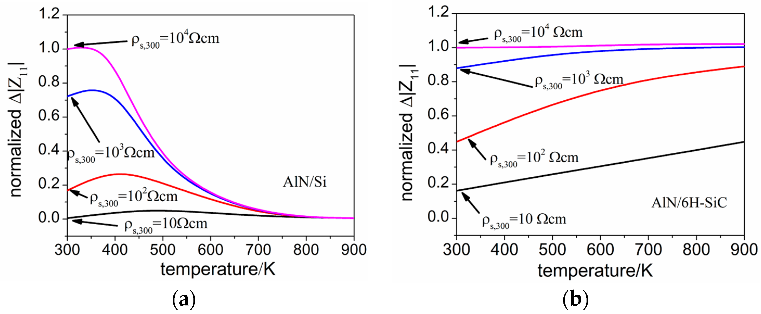
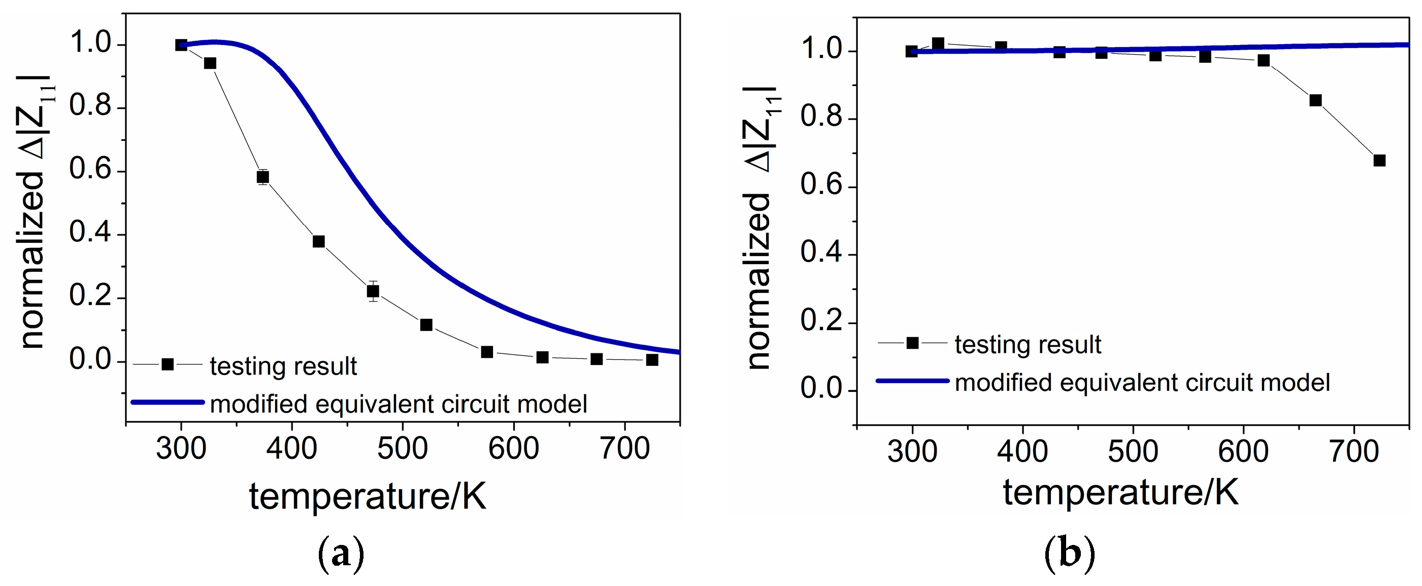
SAWRs with configurations of AlN/Si and AlN/6H-SiC are modeled within a temperature range from 300 K to 900 K, the temperature dependence of
for each configuration is calculated and normalized by using the result when
Ωcm and T = 300 K as a reference. As can be seen from
Figure 7a,b, a decrease of
is shown in AlN/Si SAWR for every initial
, while in the case of AlN/6H-SiC, opposite responses are observed, indicating a more stable device performance could be achieved by using 6H-SiC as the substrate. The contrary performances between the two configurations can be contributed to the different electrical characteristics with temperature of Si and 6H-SiC, which has been discussed above.
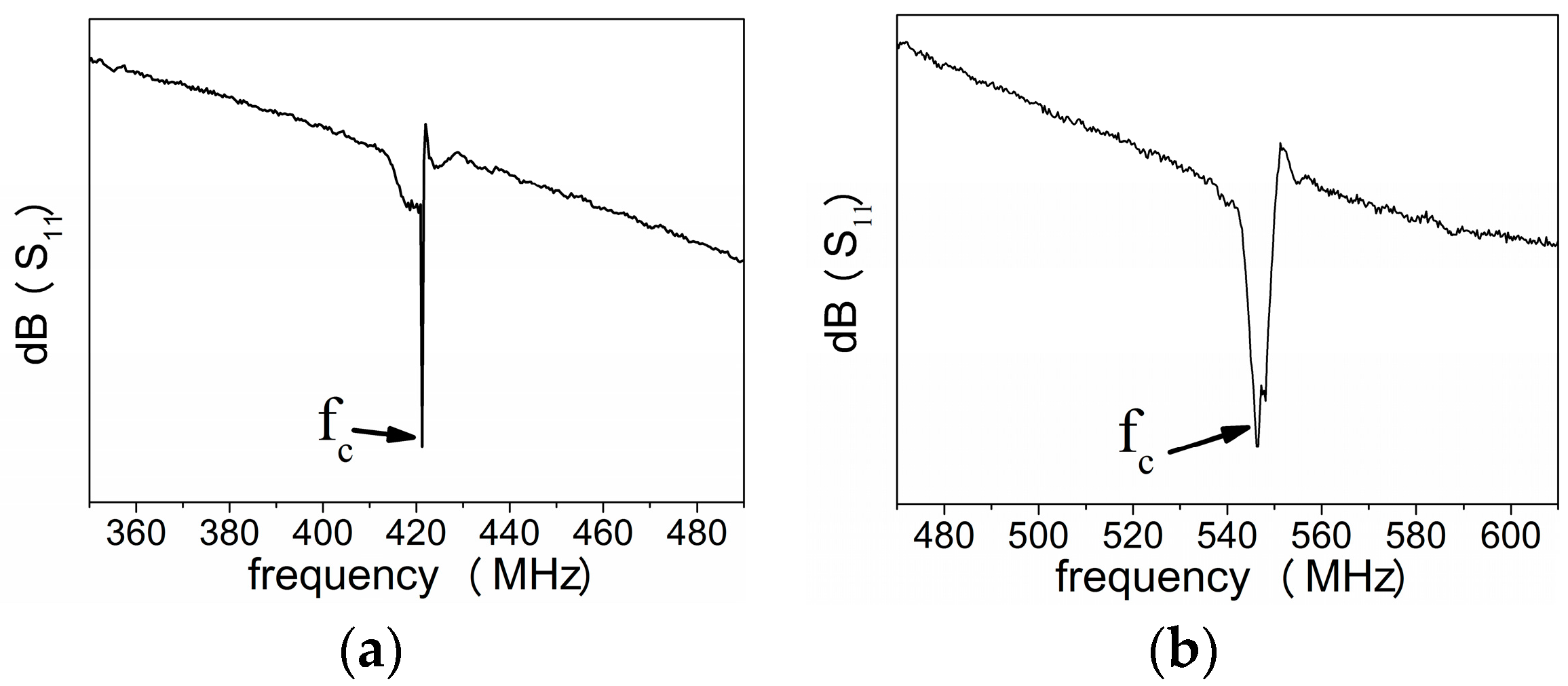
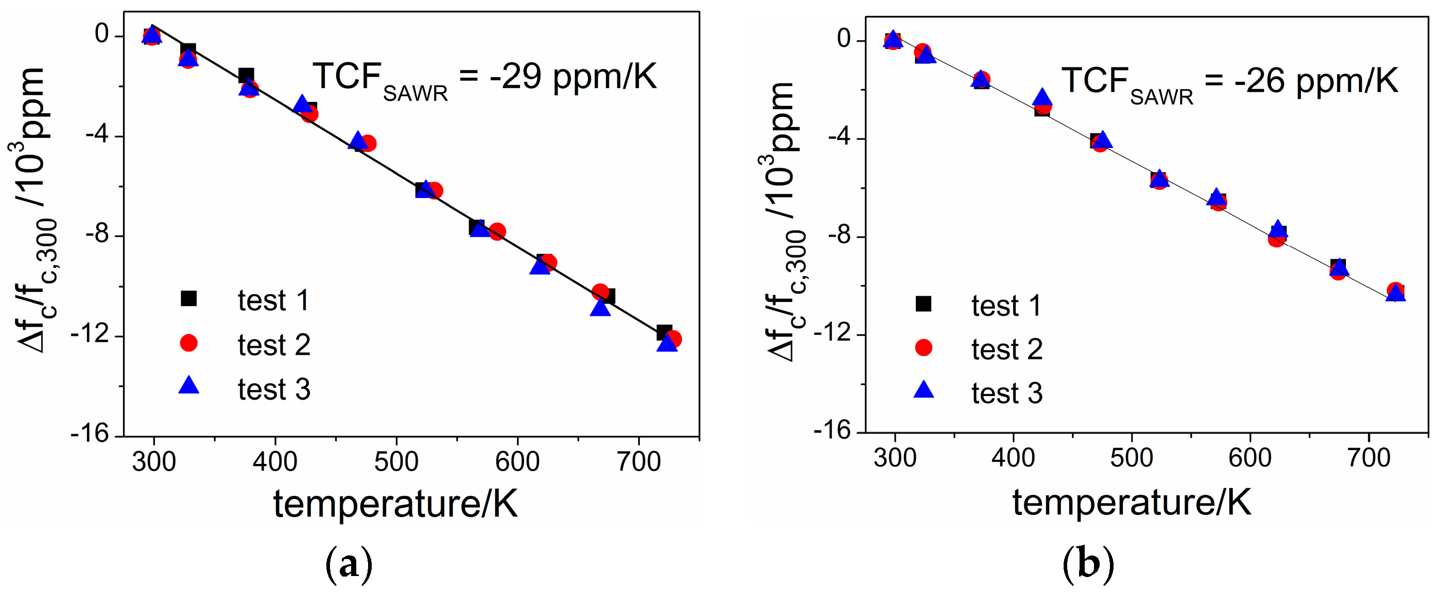
2.5. Temperature Response of Center Frequency
Except for the electrical performance of SAWR discussed in previous section, the TCF is another important parameter when evaluating the temperature response to SAWR devices. In this work, the TCF of SAWR’s center frequency (
) is analyzed theoretically and experimentally. The center frequency can be derived through the frequency domain reflection coefficient (S
11), corresponding to the frequency with the lowest S
11 as shown in
Figure 8.
For the theoretical analysis of
, it can be calculated by the SAW velocity (
) and wavelength (
as:
Considering
equals the geometric period of IDT (λ), which along with
, are all functions of temperature, therefore Equation (29) can further be expressed as:
By taking the center frequency at 300 K (
) as a reference, the TCF of SAR (
) can be expressed as:
where
and
are the SAW velocity and geometric period of IDT at 300 K, respectively.
The first term of Equation (31) represents the TCF of SAW velocity. For the hexagonal crystallized and cubic crystallized materials (Si, 6H-SiC, AlN) discussed in this work, the SAW velocity can be expressed by the mass density (
) and the elastic constants (
) as [
30,
31]:
By taking temperature into consideration,
can thus be expressed as:
where
is the mass density under temperature T and can be given by:
is the mass density at 300 K,
is the effective thermal expansion coefficient of the material along m-axis (m = x, y, z), representing the average expansion rate through 300 K to (300 +
)K, and can be calculated as:
in Equation (33) represents the elastic constants under temperature T, and can be calculated by:
For the second term of Equation (31), noticing that in the coordinate system defined in
Figure 1, SAW propagates along the x-axis, hence
can be expressed as:
By taking Equations (37) into (31), Equation (31) can further be expressed as:
The
of AlN, Si, 6H-SiC can thus be calculated and shown in
Table 3, in addition to the parameters listed in
Table A1 of
Appendix A, all other parameters used in calculation have been listed in
Table A2 of
Appendix A [
28,
29,
32,
33,
34,
35,
36].
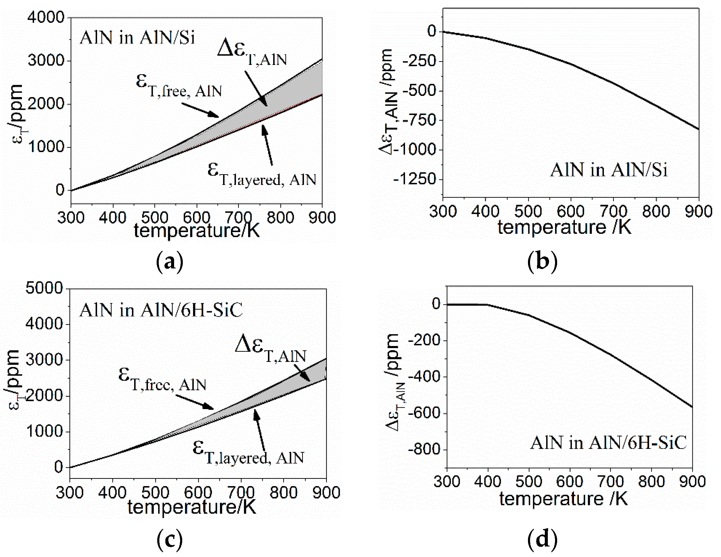
It is known that the energy of SAW is constrained within several wavelengths beneath the surface of IDT plane [
18], hence with a wavelength larger than the thickness of AlN in this work, the actual
of AlN/Si and AlN/6H-SiC based SAWR will be decided by both the piezoelectric film (AlN) and the substrate (Si or 6H-SiC). Besides, the mismatch of thermal expansions between AlN and the substrate in the x-y plane will also introduce thermal mismatch strains, namely
, which can be calculated by the thermal expansion of material in free and layered conditions, as:
where
is the ideal thermal expansion of free material, and
is the thermal expansion of material in the layered structure. Consideringthe much larger thickness of the substrate than that of AlN, the thermal expansions of the AlN/Si and AlN/6H-SiC based SAWRs are decided by the substrates, hence the thermal mismatch strains of the substrates can be neglected, and the strain of AlN is not sensitive to the film thickness, both of which has been confirmed by finite element modeling results. For each of the AlN layers in the calculated AlN/Si and AlN/6H-SiC based SAWRs, with the premise that it is isotropic in the x-y plane, the
of each configuration is calculated and shown in
Figure 9.
With the given strain field
, the relative change of
can thus be calculated by:
Therefore the TCF introduced by the thermal strain mismatch can be expressed as:
where
and
are the geometric period of IDT with strain
and without
, and has the relationship:
Similarly,
and
are, respectively, the SAW velocity under the appearance and absence of strain
. As shown in Equation (32),
can be given by the elastic constant and the mass density, which are both functions of strain field
, therefore
can be given as:
where
is the mass density under strain field and can be given by:
where
represents the elastic constants of AlN in strain field, and can be calculated by the third order elastic constants
as given by references [
36,
37,
38] and written as Equation (45) for simplicity. The third order elastic constants used for calculation has been in
Table A2 of
Appendix A.
The calculated of AlN in AlN/Si and AlN/6H-SiC configurations are −0.03 ppm/K and −0.02 ppm/K.
As can be seen, the
of AlN in both of the calculated configurations are orders of magnitude lower than the intrinsic TCF
SAW of AlN listed in
Table 3, therefore the
has little influence on the total TCF of the AlN layer in either SAWR configuration.


