
An Omnidirectional Polarization Detector Based on a Metamaterial Absorber


Abstract
:1. Introduction
2. Theory, Structure Design and Simulations
2.1. Theoretical Analysis and Structure Design
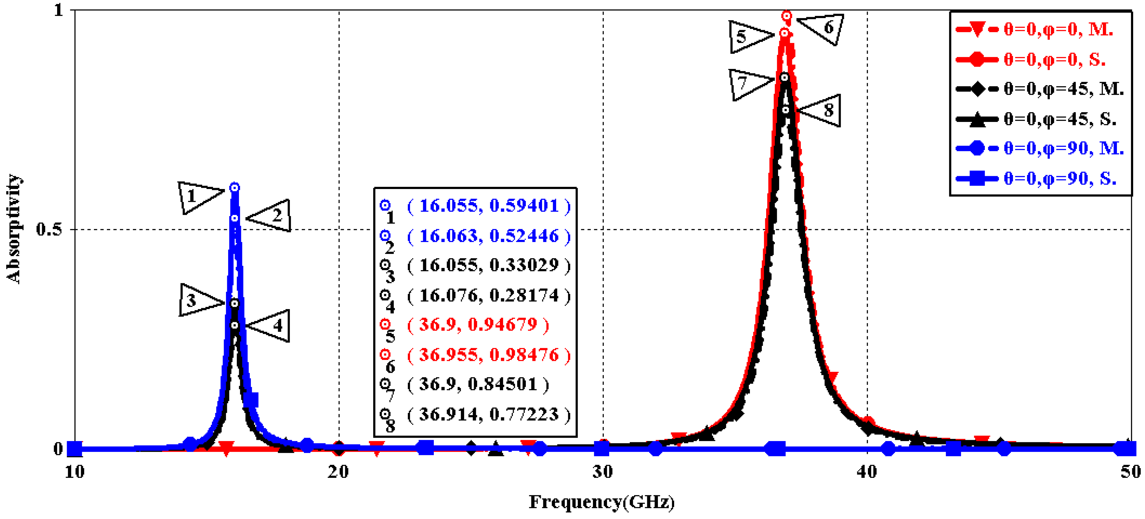
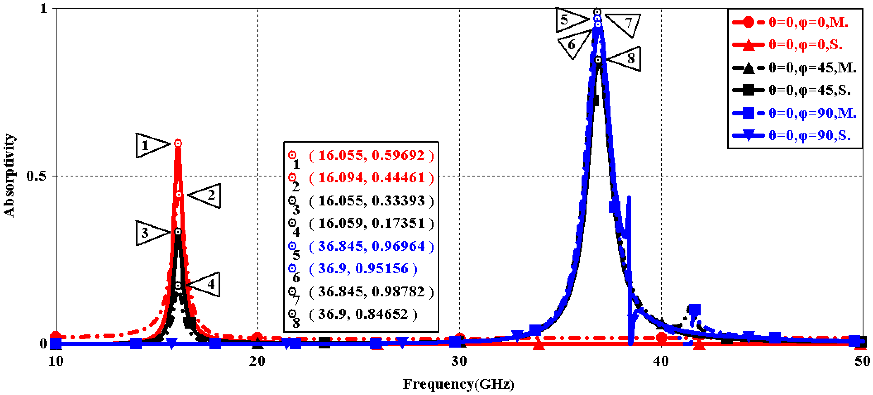
2.2. Simulation Analysis
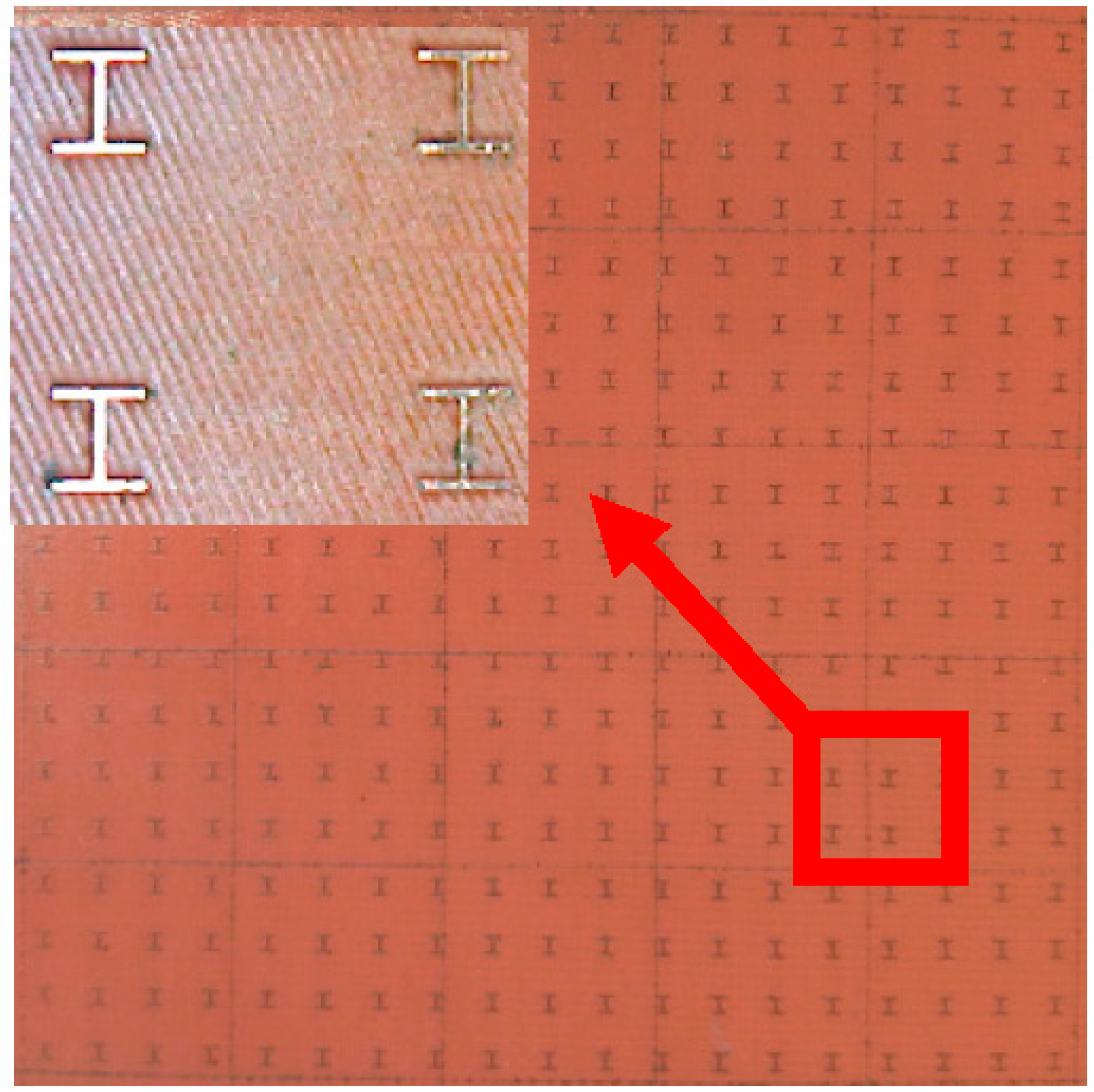
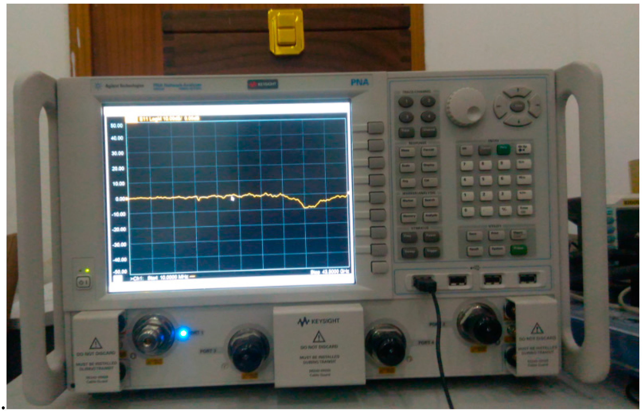
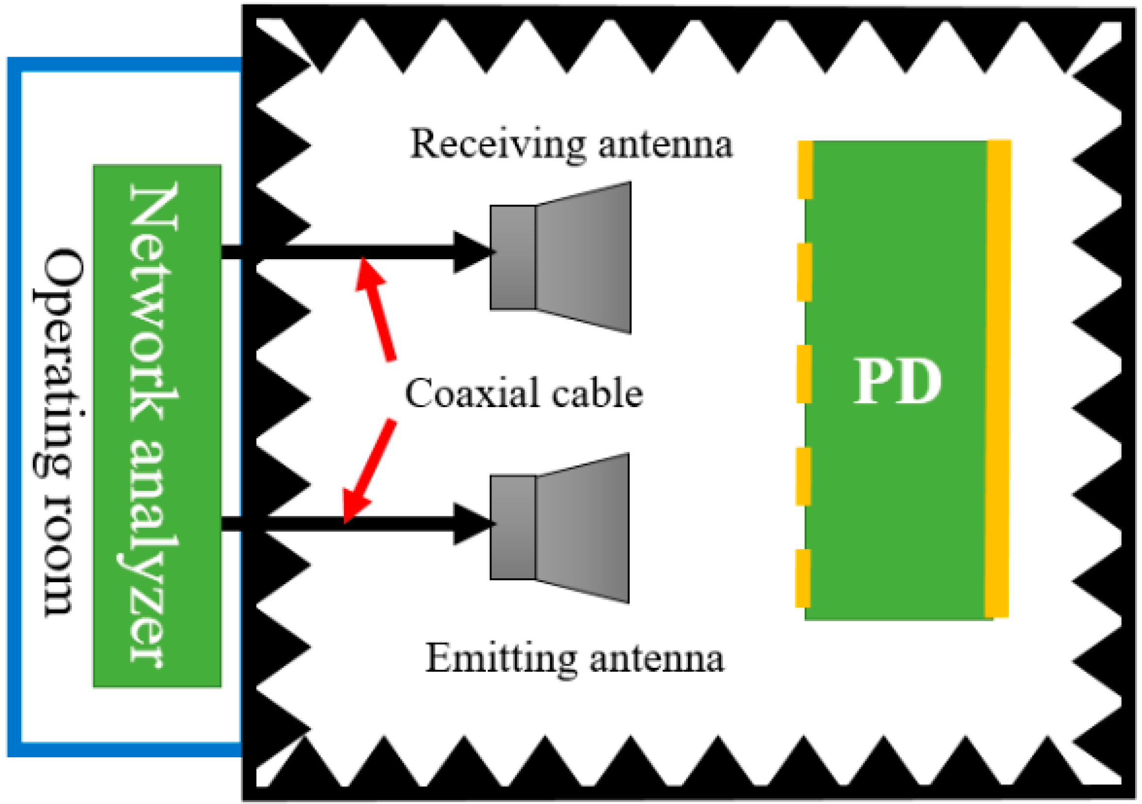
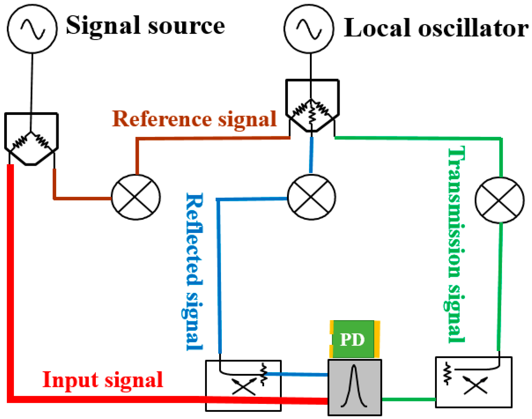
3. Processing and Testing
4. Conclusions
Acknowledgments
Author Contributions
Conflicts of Interest
Abbreviations
| PD | Polarization Detector |
| MMA | Metamaterial Absorber |
| FIT | Finite Integration Technology |
| LIGO | Laser Interferometer Gravitational Wave Observatory |
| RGWs | Relic Gravitational Waves |
| CFRPs | Carbon Fiber Reinforced Plastics |
| LHMs | Left-Handed Materials |
| TEM | Transverse Electromagnetic |
| TE | Transverse Electric |
| TM | Transverse Magnetic |
| FSS | Frequency Selective Surface |
| FWHM | Full Width at Half Maximum |
References
- Leszek, R.J.; Pawel, M. Fiber-optic interferometric polarization analyzer. In Proceedings of the IEEE Instrumentation and Measurement Technology Conference, Alaska, AK, USA, 21–23 May 2002; pp. 1497–1501.
- Peek, T.H. Dynamic polarization detection. Opt. Commun. 1971, 2, 377–382. [Google Scholar] [CrossRef]
- Azzam, R.M. Longitudinal polarization-dependent coupling of light from an optical fiber to a side-bonded planar proximity detector: Application to integrated azimuthally distributed multidetector photopolarimeters. IEEE Photonic Technol. Lett. 1980, 2, 893–895. [Google Scholar] [CrossRef]
- Azzam, R.M. Division-of-amplitude photopolarimeter (DOAP) for the simultaneous measurement of all four stokes parameters of light. Opt. Acta 1982, 29, 685–689. [Google Scholar] [CrossRef]
- Azzam, R.M.; Bashara, N.M. Ellipsometry and Polarized Light; Elsevier: Amsterdam, The Netherlands, 1987. [Google Scholar]
- Lu, S.L.; Li, G.H. Make use of stokes son space to introduce Poincare sphere. J. Qufu Norm. Univ. 1999, 25, 75–76. [Google Scholar]
- Tong, M.L.; Zhang, Y. Detecting very-high-frequency relic gravitational waves by electromagnetic wave polarizations in a waveguide. Chin. J. Astron. Astrophys. 2008, 8, 314–328. [Google Scholar] [CrossRef]
- Miao, H.X.; Zhang, Y. Analytic spectrum of relic gravitational waves modified by neutrino free streaming and dark energy. Phys. Rev. D 2007. [Google Scholar] [CrossRef]
- Grimberg, R.; Tian, G.Y. High-frequency electromagnetic non-destructive evaluation for high spatial resolution, using metamaterials. Proc. R. Soc. A 2012, 468, 3080–3099. [Google Scholar] [CrossRef]
- Grimberg, R. Electromagnetic nondestructive evaluation: Present and future. J. Mech. Eng. 2011, 57, 204–217. [Google Scholar] [CrossRef]
- Grimberg, R.; Savin, A.; Steigmann, R.; Serghiac, B.; Bruma, A. Electromagnetic non-destructive evaluation using metamaterials. Insight 2011, 53, 132–137. [Google Scholar] [CrossRef]
- Vesselago, V.G. The electrodynamics of substances with simultaneously negative values of permittivity and permeability. Sov. Phys. Usp. 1968, 10, 509–514. [Google Scholar] [CrossRef]
- Shelby, R.A.; Smith, D.R.; Schult, S. Experimental verification of a negative index of refraction. Science 2001, 292, 77–79. [Google Scholar] [CrossRef] [PubMed]
- Pendry, J.B.; Smith, D.R. Reversing light with negative refraction. Phys. Today 2004, 57, 37–39. [Google Scholar] [CrossRef]
- Luo, C.Y.; Ibanescu, M.; Johnson, S.G.; Joannopoulos, J.D. Cherenkov radiation in photonic crystals. Semin. Dial. 2003, 299, 368–371. [Google Scholar]
- Seddon, N.; Bearpark, T. Observation of the inverse doppler effect. Science 2003, 302, 1537–1539. [Google Scholar] [CrossRef] [PubMed]
- Berman, P.R. Goos-hanchen shift in negatively refractive media. Phys. Rev. E 2002. [Google Scholar] [CrossRef] [PubMed]
- Alibakhshi, K.M.; Naser, M.M.; Virdee, B.S.; Andújar, A.; Anguera, J. Compact antenna based on a composite right/left-handed transmission line. Microw. Opt. Technol. Lett. 2015, 57, 1785–1788. [Google Scholar] [CrossRef]
- Schuring, D.; Mock, J.J.; Justice, B.J. Metamaterial electromagnet cloak at microwave frequencies. Science 2006, 314, 977–980. [Google Scholar] [CrossRef] [PubMed]
- Pendry, J.B. Negative refraction and the perfect lens. Phys. Rev. Lett. 2000, 85, 3966–3969. [Google Scholar] [CrossRef] [PubMed]
- Martín, F.; Bonache, J. Application of RF-MEMS-based split ring resonators (SRRs) to the implementation of reconfigurable stopband filters: A review. Sensors 2014, 14, 22848–22863. [Google Scholar] [CrossRef] [PubMed]
- Zhang, Y.; Feng, Y.J.; Zhu, B.; Zhao, J.M.; Jiang, T. Graphene based tunable metamaterial absorber and polarization modulation in terahertz frequency. Opt. Exp. 2014, 22, 22734–22752. [Google Scholar] [CrossRef] [PubMed]
- Zou, T.B.; Hu, F.R.; Xiao, J.; Zhang, L.H.; Liu, F.; Chen, T.; Niu, J.H.; Xiong, X.M. Design of a polarization-insensitive and broadband terahertz absorber using metamaterials. Acta Phys. Sin. 2014. [Google Scholar] [CrossRef]
- Savin, A.; Steigmann, R.; Bruma, A.; Šturm, R. An electromagnetic sensor with a metamaterial lens for nondestructive evaluation of composite materials. Sensors 2015, 15, 15903–15920. [Google Scholar] [CrossRef] [PubMed]
- Tuong, P.V.; Park, J.W.; Lam, V.D.; Jang, W.H.; Nikitov, S.A.; Lee, Y.P. Dielectric and ohmic losses in perfectly absorbing metamaterials. Opt. Commun. 2013, 295, 17–20. [Google Scholar] [CrossRef]
- Costa, F.; Monorchio, A.; Manara, G. An overview of equivalent circuit modeling techniques of frequency selective surfaces and metasurfaces. Appl. Comput. Electromagn. 2014, 29, 168–183. [Google Scholar]
- Costa, F.; Genovesi, S.; Monorchio, A.; Manara, G. A circuit-based model for the interpretation of perfect metamaterial absorbers. IEEE Trans. Antennas Propag. 2013, 61, 1201–1209. [Google Scholar] [CrossRef]
- Costa, F.; Monorchio, A.; Manara, G. Analysis and design of ultra thin electromagnetic absorbers comprising resistively loaded high impedance surfaces. IEEE Trans. Antennas Propag. 2010, 58, 1551–1558. [Google Scholar] [CrossRef]
- Costa, F.; Monorchio, A.; Manara, G. Efficient analysis of frequency-selective surfaces by a simple equivalent-circuit model. IEEE Trans. Antennas Propag. 2012, 54, 35–48. [Google Scholar] [CrossRef]
- Landy, N.I.; Bingham, C.M.; Tyler, T.; Jokerst, N.; Smith, D.R.; Padilla, W.J. Design, theory, and measurement of a polarization insensitive absorber for terahertz imaging. Phys. Rev. B 2009. [Google Scholar] [CrossRef]
- Ye, Q.W.; Liu, Y.; Lin, H.; Li, M.H.; Yang, H.L. Multi-band metamaterial absorber made of multi-gap SRRs structure. Appl. Phys. A 2012, 107, 155–160. [Google Scholar] [CrossRef]


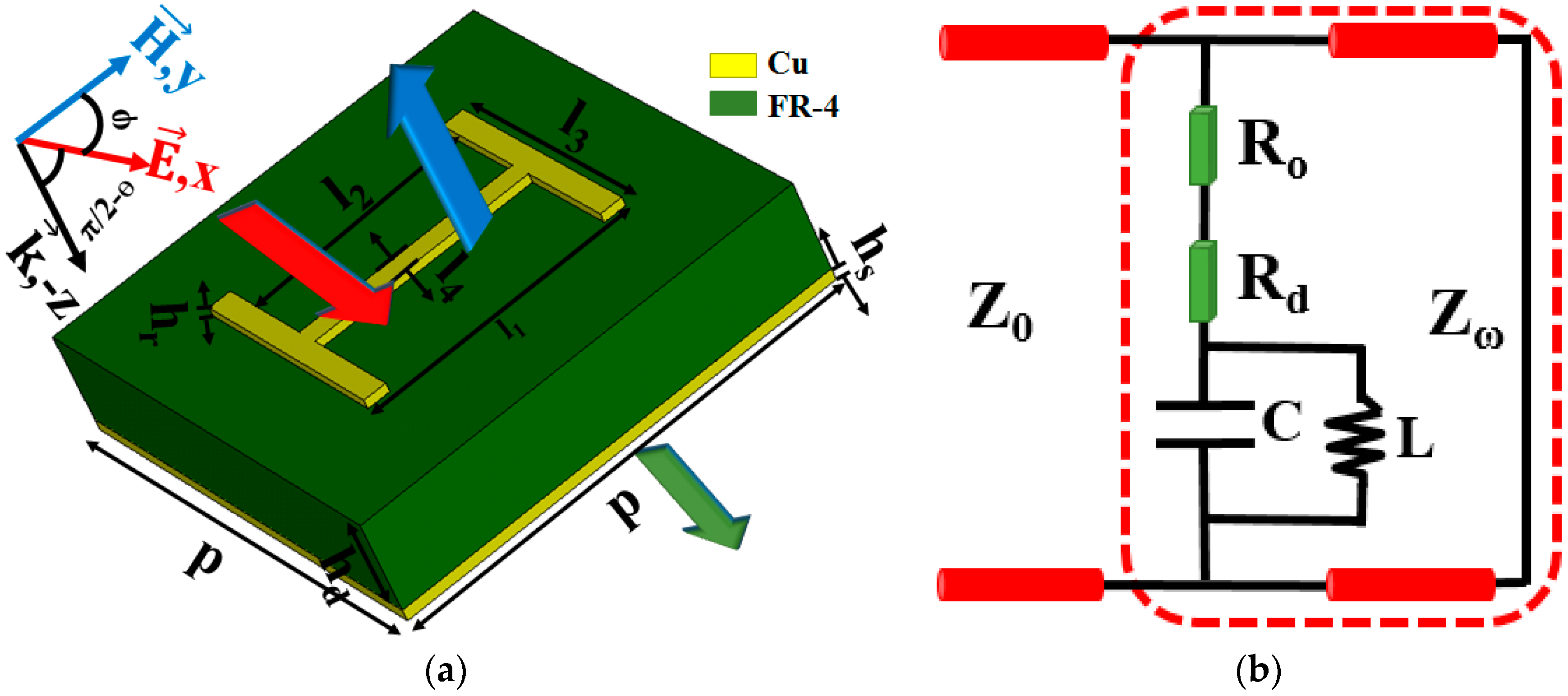
| Parameters | Value (μm) | Description |
|---|---|---|
| p | 4000 | periodic array length |
| hs | 0.3 | substrate thickness |
| hd | 200 | dielectric thickness |
| hr | 0.1 | metasurface thickness |
| l1 | 1200 | “I” dimension |
| l2 | 1000 | “I” dimension |
| l3 | 1000 | “I” dimension |
| l4 | 100 | “I” dimension |
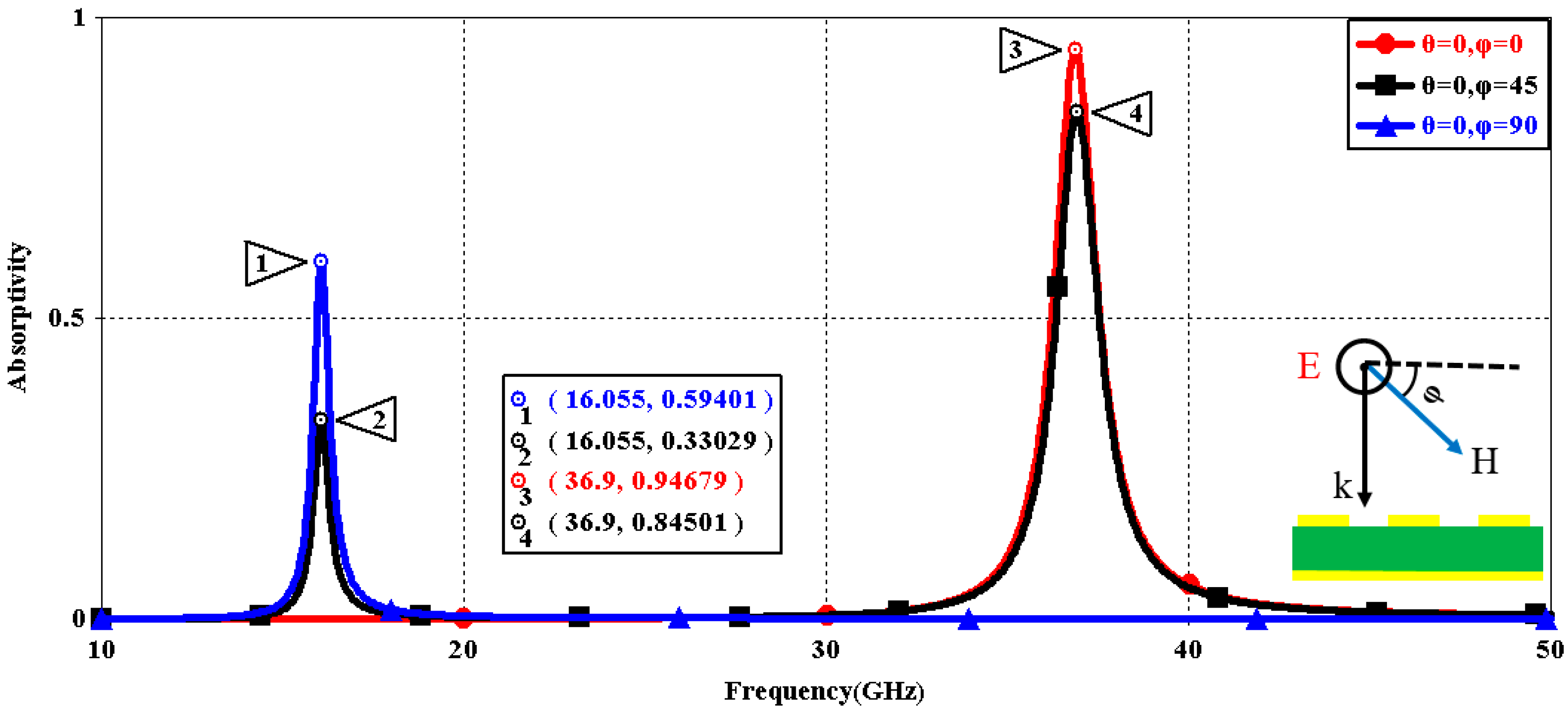
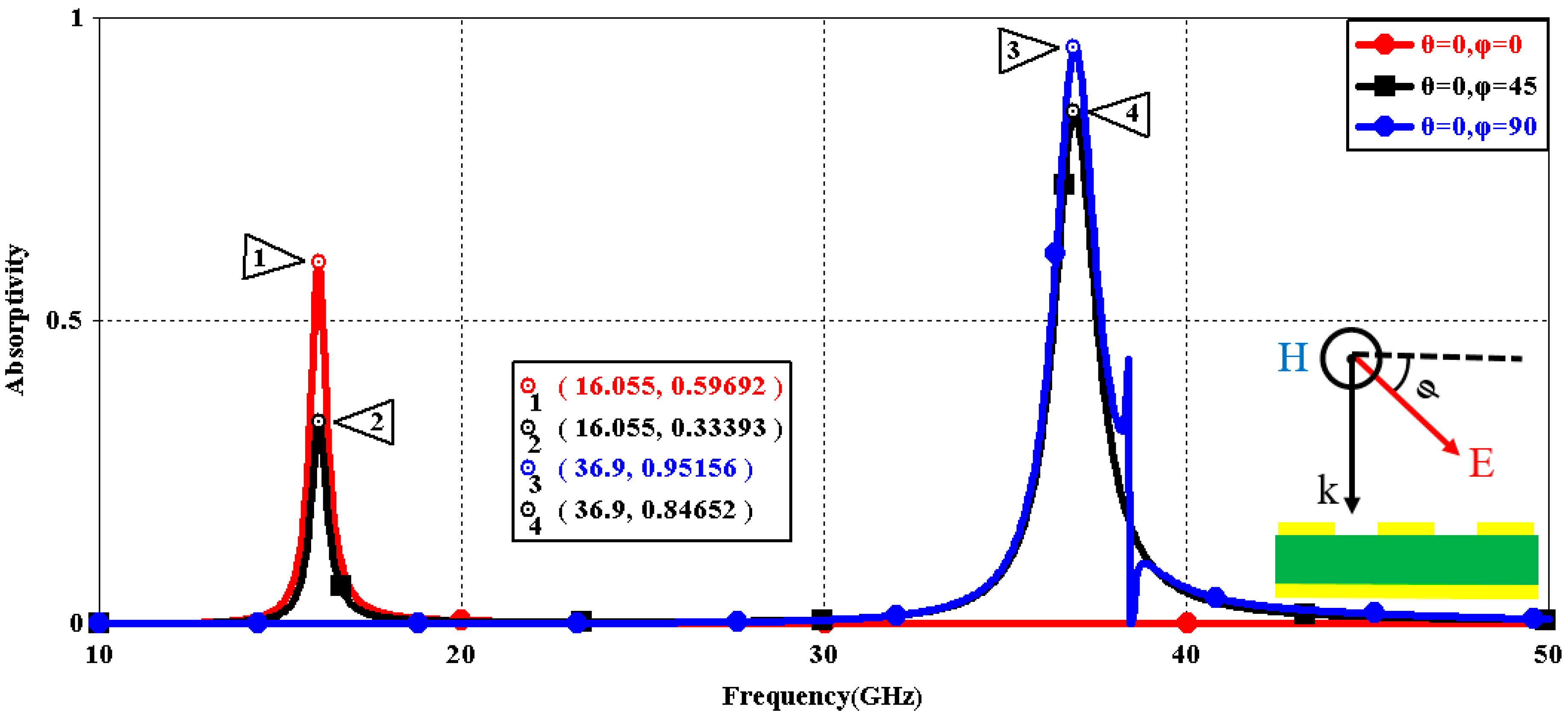
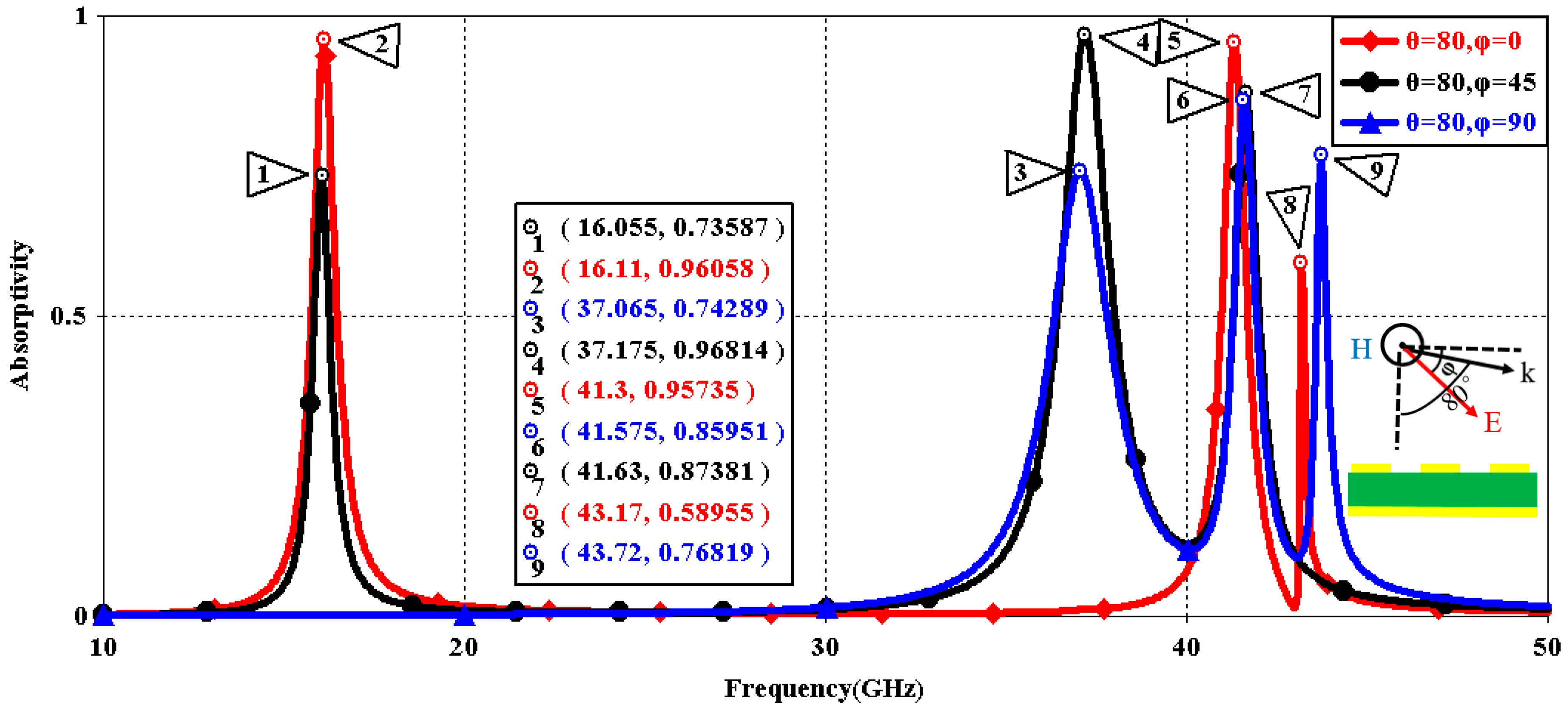
| Resonance Frequency (GHz) | Absorptivity | Polarization |
|---|---|---|
| 36.9 | 0.94679 | TE, θ = 0°, = 0° |
| 16.055, 36.9 | 0.33029, 0.84501 | TE, θ = 0°, = 45° |
| 16.055 | 0.59401 | TE, θ = 0°, = 90° |
| 16.055 | 0.59692 | TM, θ = 0°, = 0° |
| 16.055, 36.9 | 0.33393, 0.84652 | TM, θ = 0°, = 45° |
| 36.9 | 0.95156 | TM, θ = 0°, = 90° |
| 36.9 | 0.99802 | TE, θ = 40°, = 0° |
| 16.055, 36.9 | 0.25826, 0.71298 | TE, θ = 40°, = 45° |
| 16.055 | 0.48603 | TE, θ = 40°, = 90° |
| 16.055, 41.41 | 0.6038, 0.42432 | TM, θ = 40°, = 0° |
| 16.055, 36.9, 41.355 | 0.34933, 0.87621, 0.31582 | TM, θ = 40°, = 45° |
| 36.845 | 0.96439 | TM, θ = 40°, = 90° |
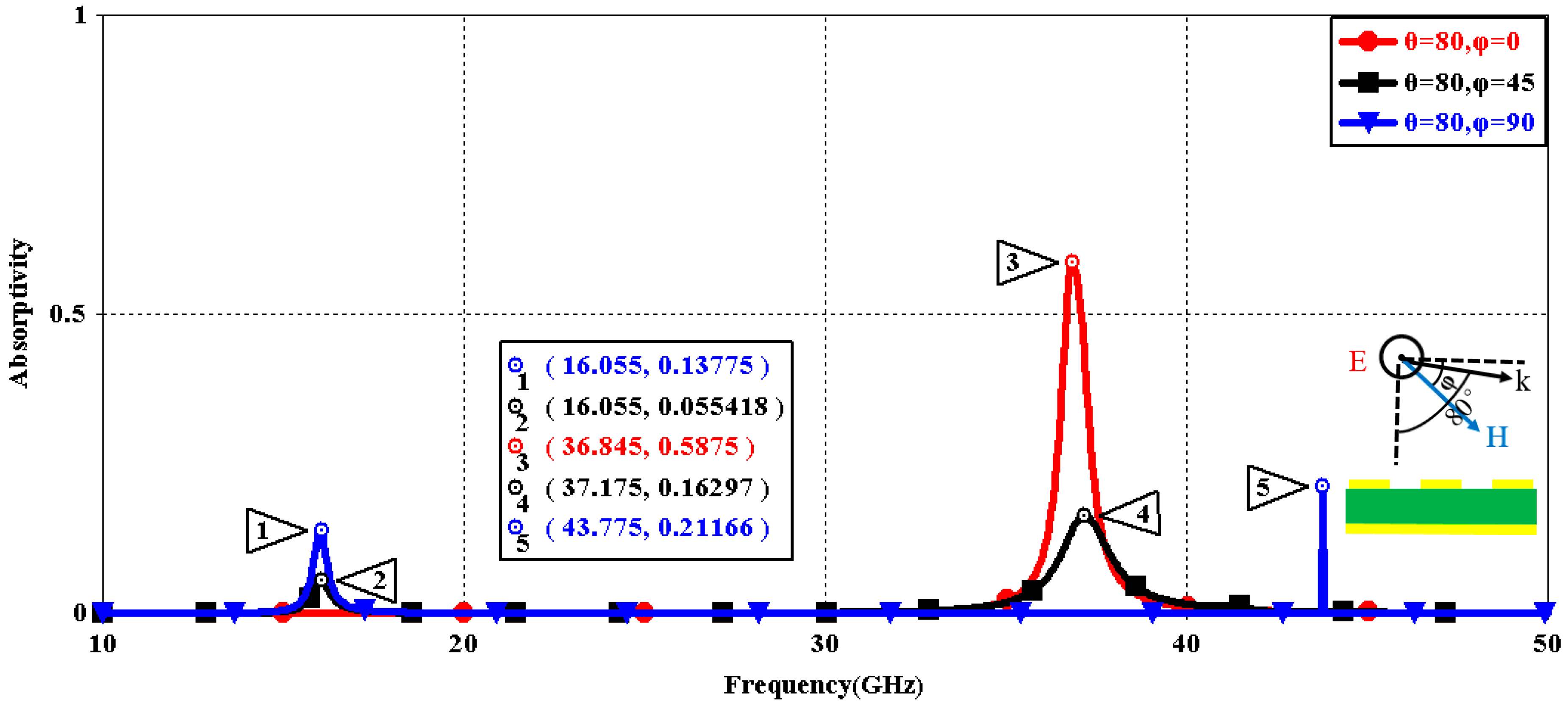
| 36.845 | 0.5875 | TE, θ = 80°, = 0° |
| 16.055, 37.175 | 0.055418, 0.16297 | TE, θ = 80°, = 45° |
| 16.055, 43.775 | 0.13775, 0.21166 | TE, θ = 80°, = 90° |
| 16.11, 41.3, 43.17 | 0.96058, 0.95735, 0.58955 | TM, θ = 80°, = 0° |
| 16.055, 37.175, 41.63 | 0.73587, 0.96814, 0.87381 | TM, θ = 80°, = 45° |
| 37.065, 41.575, 43.72 | 0.74289, 0.85951, 0.76819 | TM, θ = 80°, = 90° |
© 2016 by the authors; licensee MDPI, Basel, Switzerland. This article is an open access article distributed under the terms and conditions of the Creative Commons Attribution (CC-BY) license (http://creativecommons.org/licenses/by/4.0/).
Share and Cite
Zhang, B.; Zhang, Y.; Duan, J.; Zhang, W.; Wang, W. An Omnidirectional Polarization Detector Based on a Metamaterial Absorber. Sensors 2016, 16, 1153. https://doi.org/10.3390/s16081153
Zhang B, Zhang Y, Duan J, Zhang W, Wang W. An Omnidirectional Polarization Detector Based on a Metamaterial Absorber. Sensors. 2016; 16(8):1153. https://doi.org/10.3390/s16081153
Chicago/Turabian StyleZhang, Binzhen, Yong Zhang, Junping Duan, Wendong Zhang, and Wanjun Wang. 2016. "An Omnidirectional Polarization Detector Based on a Metamaterial Absorber" Sensors 16, no. 8: 1153. https://doi.org/10.3390/s16081153