TiO2 Nanotubes: Recent Advances in Synthesis and Gas Sensing Properties


Abstract
: Synthesis—particularly by electrochemical anodization-, growth mechanism and chemical sensing properties of pure, doped and mixed titania tubular arrays are reviewed. The first part deals on how anodization parameters affect the size, shape and morphology of titania nanotubes. In the second part fabrication of sensing devices based on titania nanotubes is presented, together with their most notable gas sensing performances. Doping largely improves conductivity and enhances gas sensing performances of TiO2 nanotubes.1. Introduction
The development of portable and low cost gas sensors with high sensitivity, selectivity, and low working temperature is highly desirable and still a great challenge. Metal oxides are attractive materials for the fabrication of gas sensing devices because of their obvious advantages, such as low cost, production flexibility, and good thermal and chemical stability [1,2]. Especially hierarchical nanostructured metal oxides with the different morphologies are good candidates for the manufacture of gas sensors.
The conductivity of metal oxide nanostructures changes with the surface adsorption and desorption of gas molecules. This change is caused by the electronic transfer that occurs upon the adsorption of gas molecules over the film surface [3,4]. These conductivity changes strongly depend on the shape and the size of the nanostructures. Recently TiO2 nanostructures with the different shapes have received extensive attention from the gas sensing research community due to their unique physical and chemical properties [5–9], and nanostructured titania with tubular shape has been considered one of the most promising materials for the fabrication of gas sensing devices [10].
The gas sensitivity can be enhanced by the large surface area and the morphology of tubular structures. For reproducibility of the functional properties of gas sensors the preparation of highly ordered nanostructures is also an important factor. Investigations have shown that titania nanotubes are sensitive mainly towards hydrogen [11,12]. To expand the applications of titania nanostructures in the fabrication of chemical sensors there are number of parameters that need to be improved, namely the conductance of TiO2 in air, the sensing signal, the response and the recovery times.
Extensive efforts have been made to extend the functionalities of titania by modifying the band structure with dopant materials [13–19]. Investigations show that doped and mixed structures of titania are emerging as important materials for the improvement of conductometric sensors' properties [20–27]. The change of carrier density by different dopants in polycrystalline TiO2 has been investigated. A typical dopant is Nb, which acts as a shallow donor in TiO2 [28,29]. Compared to other dopants such as Pt, carbon nanotubes, Pd, P and Ni [18,20,21,26], the similarity of the radii of Nb+5 (r = 0.70 Å) and Ti+4 (r = 0.68 Å) allows Ti atoms to be replaced by Nb in the lattice [30]. Chemical sensors operate on the basis of the adsorption and removal of oxygen on the surface of the material. To enhance this adsorption/desorption effect on the TiO2 surface the working temperature of the sensing layer must be higher than the normal ambient air temperature, but the phase transformation from anatase to rutile at high temperature ranges can cause a drastic decrease in sensor properties [31], as it has been found that the anatase phase of titania is more reactive than the rutile one [32–34]. The experimental results have shown that the presence of substituted Nb ions in the anatase structure of TiO2 inhibits the undesirable phase transition of the structure [30], so to enhance the conductivity and to stabilize the gas sensing properties of titania Nb is more preferable compared to other dopants.
The development of fabrication technics for the synthesis of highly ordered doped or mixed titania nanostructures is very current. Since the formation of titanium dioxide nanotubes by electrochemical deposition in a mould was reported in 1996 [35], numerous investigations have been carried out to develop fabrication methods for titania tubular structures. The present review is focused on the recent developments in the synthesis, modifications and gas sensing properties of titania nanotubes which can open new perspectives for the fabrication of gas sensors.
2. Synthesis of Titania Nanotubes
A few approaches have been employed for synthesis of titania tubular structures such as electrochemical anodization [36–39], atomic layer deposition (ALD) [40–42] and hydrothermal synthesis [43–45]. Detailed description of the preparation methods is given in Table 1. For the preparation of TiO2 nanotubes by means of ADL it is necessary to use a porous template. High quality nanoporous anodic aluminum oxide is usually used as template to promote the growth of titania nanotubes by ADL. The template-assisted technique may limit the choice of the substrate and requires post-processing separation of the obtained tubular arrays from the template. In addition part of the tubes may break off from the substrate during the template removal [40]. Hydrothermal synthesis is a method consisting of hydrothermal treatment of solutions of anatase and rutile titania powders and post-growth annealing. Preparation of titania nanotubes by means of electrochemical anodization refers to the anodic formation of titania nanotubes by oxidation and etching of metallic titanium. The method, described below in detail, allows direct growth of the TiO2 tubular arrays on different types of substrates and the modification of the surface structure of titania at room temperature [39,46].
2.1. Anodic Formation of Titania Nanotubes
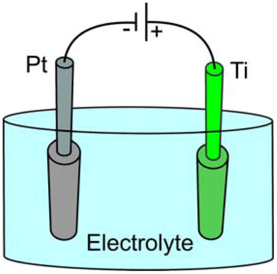
Electrochemical anodization of titanium is a relatively simple and efficient process to fabricate well-aligned and highly ordered TiO2 tubular structures. Anodization is carried out in a two-electrode system and the process is controlled by variation of the anodization parameters (Figure 1).
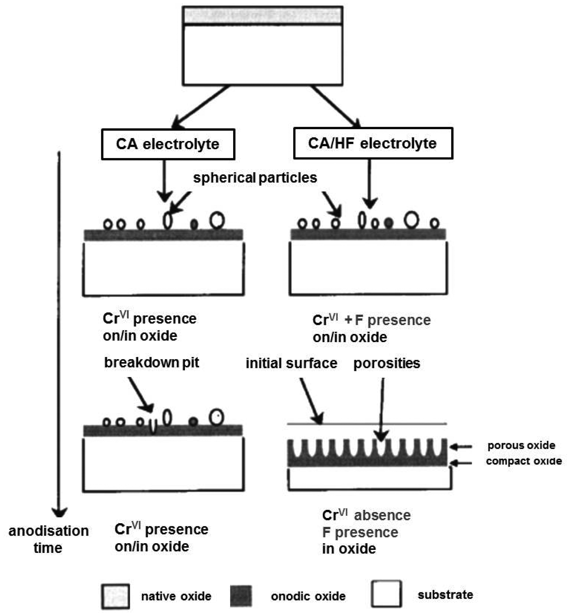
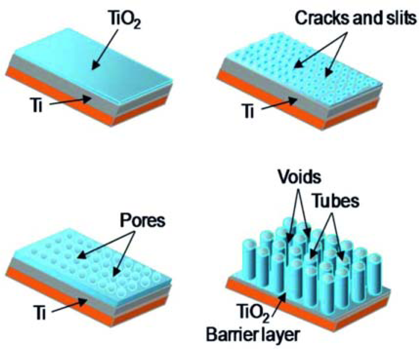
Preparation of titania tubular arrays by means of the anodization method in chromic acid solution both without and with hydrofluoric (HF) acid addition was performed for the first time by Zwilling et al. in 1997 [48,49]. The potential between the specimen and a titanium cathode was increased from 0 to 5 or 10 V in five equal steps of 1 min each. Zero volts means that the anode and the cathode were short-circuited. Then the specimen was maintained at the final voltage for variable times ranging between 1 and 55 min; some experiments were performed by reaching the final voltage in a single step. Non-porous oxide compact films were formed after the anodization of titanium and titanium alloy in chromic acid without HF and a duplex film composed of a compact layer surmounted by a columnar porous layer have been formed in chromic acid containing HF. When fluorine was not present the Cr(VI) species played a poisoning role and stopped the growth of the compact non-porous layer formed in chromic acid media (Figure 2) [49].
In HF-containing solution the fluorine ions played an antidote role and the local competition between Cr(VI) and F− species led to a continuous growth of the porous structure (Figure 2). The consistency of the oxygen content was explained by a compensation between film thickening and pore extension due to the competition between dissolution and growth [49]. Thus, the oxidation and the dissolution of the metal are the key processes for the formation of titania nanotubes by electrochemical anodization. The anodization process can be described as follows: in the first step an oxide barrier layer is formed on the electrolyte-metal interface [39,50]:
Then cracks and narrow slits appear on the surface due to field-enhanced dissolution of the oxide layer. Diffusion of the electrolyte into these cracks and slits enhances the dissolution rate compared with other areas:
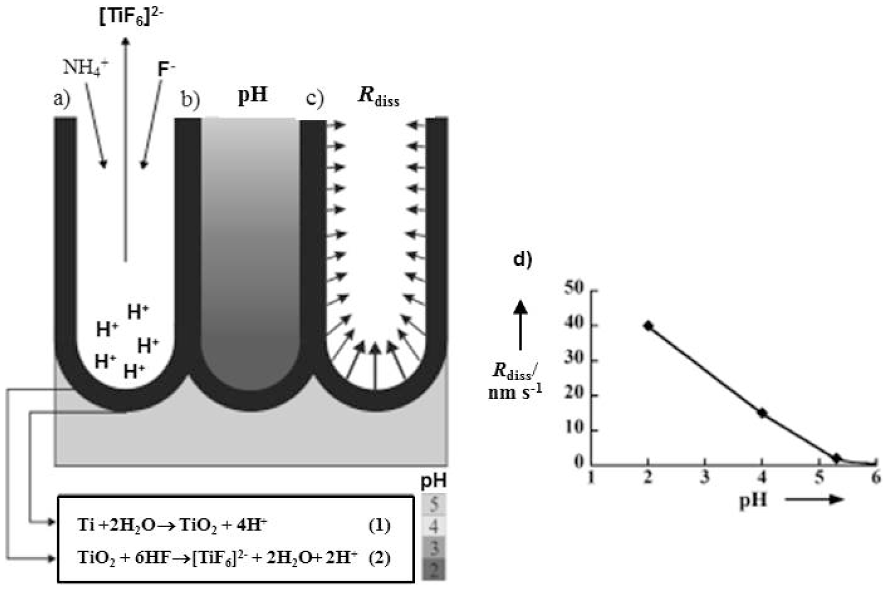
The growth of nanotubes is related to the diffusion of F− ions through the oxide layer and effusion of [TiF6] 2−. Therefore by variation of the content of water and fluorine ions in the electrolyte it is possible to control the titanium anodization process [39,50]. Cracks enlarge and become connected with neighboring cracks. Initial pores are formed in the cracks. Then a random formation of a porous structure in the cracks and slits occurs (Figure 3). As the anodization proceeds, the interpore regions are also attacked by the F− ions. Therefore slits are generated at those parts. The growth of those slits leads to the formation of parallel tube-like arrays [39].
Morphological and structural studies show that the rates of the reactions (1) and (2) are strongly affected by the type and the pH of the electrolyte, the applied voltage (or current) and the anodization temperature. In reaction (1) the Gibbs free energy ΔGel change obeys the Nernst equation and is a function of the electrode potential; ΔGel = −zFE (3) where z is the electron transfer number, F is the Faraday constant, and E is the electrode potential, which is changed by the applied voltage [51]. In the electrochemical cell most of the applied voltage is consumed in the current–resistance drop of the conducting medium and a relatively small fraction of it manifests as the polarization potential on the electrodes. The absolute value of the over-potential on electrode is expected to increase with increasing applied voltage. The chemical dissolution of TiO2 occurs via reaction (2). Fluoride ion is a potent species that can break down metal oxides, i.e., cause metal oxide dissolution reactions when Gibbs free energy change is negative (ΔG0ch). ΔGch is Gibbs free energy change of chemical dissolution of the metal oxide. When ΔGch < ΔGel < 0, the metal oxide formed is protected by the electrical potential against chemical dissolution. In the proximity of the cross-point between ΔGel and ΔGch, the anodized metal oxide is in part dissolved and in part protected, leading to the formation of a porous oxide [51], hence the geometrical parameters of the resulting titania tubular structures are strongly affected by the anodization conditions.
Further the formation of porous TiO2 on titanium was investigated in aqueous solutions of HF and H2SO4/HF electrolyte [36,52]. In aqueous solution of HF the titanium oxide nanotube arrays were obtained under anodizing voltages ranging from 10 to 40 V. In all cases, the final length of the nanotubes was not affected by the anodizing time [36]. Beranek et al. also prepared highly ordered porous TiO2 with single pore diameters of 140 nm in H2SO4/HF electrolyte. During the formation process, significant current oscillations were observed with an amplitude which depended strongly on the HF content of the electrolyte. Investigations had shown that due to the high rate of chemical dissolution of TiO2 in this solution, the nanotubes grown up to a limiting thickness of ∼500 nm [37].
Afterwards Macak et al. reported that the chemical dissolution rate of TiO2 is highly dependent on the pH value of the electrolyte [52]. They demonstrated that the thickness of the porous layer is essentially the result of equilibrium between the electrochemical formation of TiO2 at the pore bottom and the chemical dissolution of this TiO2 in an F− ion containing solution (Figure 4). Paulose et al. confirmed that the nanotube length is a function of both pH and the anodization voltage. By increasing voltage at a given pH value the tube length and the pore size were increased (Table 2) [8].
Varghese et al. increased the thickness of tubular layer by anodization of titanium in fluorine-containing dimethyl sulphoxide (DMSO) electrolyte [53]. The length of tubes was between 0.3 and 33.0 μm. During the experiments ethylene glycol (EG) was also used as an electrolyte besides the fluorine-containing DMSO. They found that the conductivity of an electrolyte composed of hydrofluoric acid (HF) and DMSO is originally low, but can be enhanced substantially by applying an electric field between two immersed electrodes and the oxide dissolution rate during anodization of titanium films in this electrolyte is proportional to its conductivity. To obtain longer nanotubes, the electrolyte conductivity should be lower. DMSO was found to be optimal for obtaining nanotubes of high structural and optical quality with a wide range of lengths compared to EG-based electrolytes.
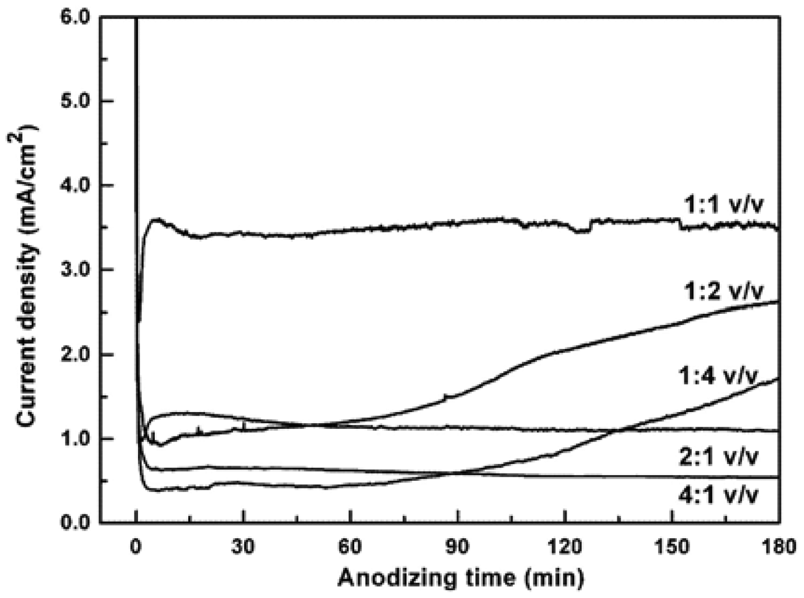
Lai et al. investigated the growth rate of TiO2 nanotube arrays in novel organic–inorganic electrolyte system [38]. The electrolytes were 0.5 wt% NaF and 0.2 M Na2SO4 in a mixed solution containing glycerol (1,2,3-propanetriol) and deionized (DI) water. Dimensions and morphology of the anodized TiO2 were strongly dependent, on the volumetric ratios of glycerol versus water, besides on the applied potential and the anodizing time. The current density-anodizing curve was recorded during the anodization of Ti foil in the water–glycerol electrolyte for different volumetric ratios at 10 V (Figure 5). The values of current densities were significantly different, thus the growth rates of TiO2 nanotube arrays were strongly different.
Wang et al. reported that in non-aqueous electrolyte the TiO2 nanotube dimensions are affected by the electrolyte temperature [54]. They anodized titanium foil in aqueous (i.e., 0.5 wt% hydrofluoric acid in DI water) and nonaqueous electrolytes (i.e., glycerol containing ammonium fluoride); Anodization was performed at room temperature and inside an ice bath. According to the obtained results in nonaqueous electrolyte (i.e., glycerol), the nanotube diameter is markedly affected by the electrolyte temperature (Figure 6). At lower temperature (i.e., in the ice bath), the fluorine ion mobility in the viscous glycerol electrolyte was further suppressed, resulting in much slower etching of formed TiO2, which in turn led to a smaller nanotube diameter.
Recently Galstyan et al. have used different kind of electrolyte to investigate the effect of ion mobility on the anodization process [39]. H2SO4 aqueous solution (0.5–1 M) and H2O in glycerol (1–5 M) with NH4F (0.5–1 wt%) have been used as electrolytes. Nanotubular and nanoporous TiO2 structures have been prepared on different substrates by anodization of Ti films. For the fabrication of the tubular and the porous structures the anodization has been carried out in constant voltage (potentiostatic) mode and constant current (galvanostatic) mode at 20 °C.
Well-aligned TiO2 nanotubes have been obtained in glycerol-based electrolyte by potentiostatic mode on a variety of different substrates: flexible polyethylene terephthalate (PET), smooth and rough alumina, and titanium sheet. Nanoporous structures have been obtained in H2SO4 aqueous solution by potentiostatic mode.
Porosity and pore diameter were strongly dependent on current density and anodization time. In H2SO4-containing aqueous electrolyte a variation in pore size up to ∼80 nm has been obtained, while in NH4F-containing glycerol electrolyte the variation has been no more than 30 nm. The anodization process is slow for NH4F-containing glycerol electrolyte due to the high dielectric constant and coefficient of viscosity, hence the dependence of the diffusion constant on the viscosity follows the Stokes–Einstein equation: D = kBT/(6πηrs), where D is the translational diffusion coefficient, kB is Boltzmann's constant, T is the absolute temperature, η is the dynamic viscosity, and rs is the radius of a spherical body. According to this formula, D is inversely proportional to η, therefore the differences between pore diameters for the samples anodized in NH4F-containing glycerol electrolyte has been less than in H2SO4 aqueous electrolyte, due to the different viscosity of the two solutions.
The influence of the electrolyte viscosity on the growth rate of TiO2 nanotubes was also investigated by Sreekantan et al. [50]. Anodization was carried out in ethylene glycol- (η = 16 cP at 25 °C) and glycerol (η = 945 cP at 25 °C)-based electrolytes. The growth rate of the nanotubes was higher in ethylene glycol because of it's low viscosity. The length of nanotubes was increased when 1 wt% water was added to the ethylene glycol, but when water content was increased to 2 wt% the length of tubes decreased. The calculated rate of formation was approximately 308 nm min−1.
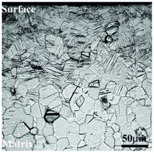
Another important factor for the formation of TiO2 nanotube arrays is the substrate microstructure. Pure titanium subjected to surface mechanical attrition treatment (SMAT-Ti) (Figure 7) and untreated were anodized in a glycol solution containing NH4F and small amounts of water [55]. Ti plates were annealed at 750 °C for 5 h to eliminate any residual deformation. After the annealing, they were ground to remove oxide and polished to a mirror finish. For each anodizing period the thickness of the TiO2 layer on SMATed-Ti was much thicker than that on unSMATed-Ti. The authors mentioned that nanocrystallized Ti is propitious to the growth of TiO2 nanotubes; grain boundaries and dislocations play the leading role in accelerating reaction rate and ion diffusion coefficient during anodization. The nanotube layers on unSMATed-Ti and SMATed-Ti were composed of amorphous TiO2. Nanocrystallization of Ti changed the surface morphologies and the phase components of TiO2 nanotubes.
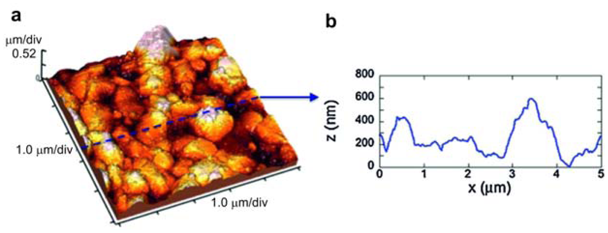
Galstyan et al. studied how surface roughness of the substrates affects the morphology of TiO2 nanotubular arrays [46]. For the morphological analysis nanotubes were obtained on stiff and flexible substrates with different surface roughnesses. Initially metallic titanium films were deposited on flexible (Kapton® HN) and rough alumina substrates by means of RF (13.56 MHz) magnetron sputtering. Then the tubular arrays of TiO2 were prepared by electrochemical anodization in a glycerol- based electrolyte.
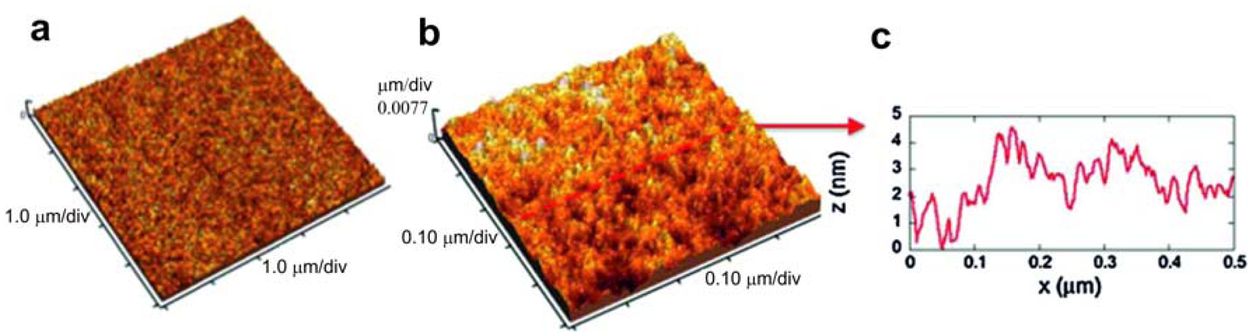
The surface analysis of the substrates showed a surface structure of stiff substrates composed by grains (alumina with the granular morphology) with measured sizes ranging from hundreds of nm to 1 μm (Figure 8), giving the substrate an RMS (root mean square) roughness of about 105 nm. Differently, the flexible polymeric substrate showed an almost flat surface (Figure 9) with an RMS roughness lower than 1 nm. Its morphology is better visualized in Figures 9b,c, where the 0.5 μm × 0.5 μm scan and a profile acquired along with it show the granularity of the polymer at the nanoscale, with grains having measured sizes of a few nm. SEM observations showed that well-aligned smooth tubes with a homogeneous distribution were obtained on both the substrates.
Nanotubes obtained on the granular surface of alumina substrates grew as a bunch of tubes on every grain. On the flexible substrate the same tube growth behavior did not take place due to the low roughness of the substrate, thus the surface roughness of the substrate also has an appreciable influence on the morphology of the resulting TiO2 tubular arrays.
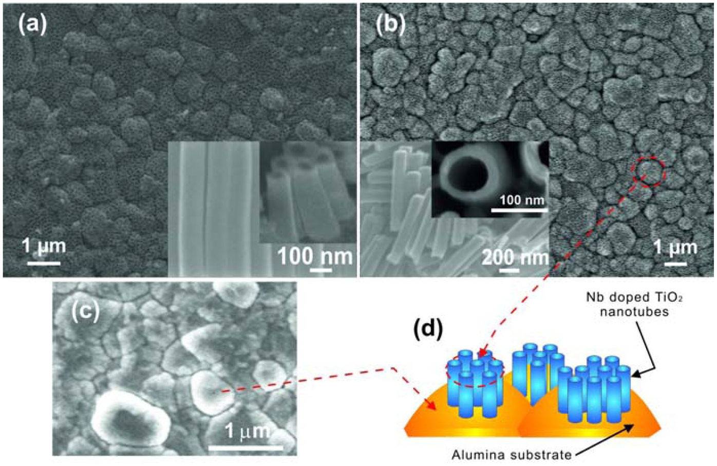
In another work Galstyan et al. reported the properties of pure and doped TiO2 nanotubes prepared on a granular alumina surface with lateral dimensions of grains ranging between 200 and 1,200 nm [47]. Straight nanometric tubes were obtained on alumina decorating the grains of the substrate surface (Figure 10). The morphology of the tubular arrays formed on alumina [47] is different from those that are grown on Kapton® HN [46], but the distribution of tubes on both types of substrates is very homogenous.
Although the experimental results demonstrate that the electrochemical anodization method is a very convenient method for the modification of the surface structure of titania and allows obtaining highly ordered tubular arrays, the as-prepared structures are mainly amorphous. Usually the crystallization of the structures is carried out by post-growth annealing [38,47,54,56]. The amorphous to anatase or rutile phase transition is made possible by a variety of annealing regimes. The conversion from amorphous to crystalline anatase phase takes place at approximately 300 °C. The rutile phase appears at approximately 500 °C and becomes the dominant phase at 600 °C [56]. Improvement of structural and functional properties of titania nanostructures is an important issue for the fabrication of highly sensitive and selective sensing devices with a low working temperature. As we have mentioned above, the conductivity of chemical sensors changes due to the interaction between the sensing layer and gas molecules [3,4,9], therefore controlling the electronic, morphological and chemical properties of the sensing material, namely band-gap, Fermi level position, dispersion of catalyst, size of crystallites and their network connection is fundamental to enhance the sensitivity of chemoresistive devices [57–59]. Along with the development of geometrical parameters of TiO2 nanotubes recent research has concentrated on the enhancement of their structural and functional properties. Below recent advances in the fabrication of doped, mixed and modified TiO2 nanotubes that may improve the sensing properties of titania tubular structures are reported.
2.2. Fabrication of Doped, Mixed and Modified Titania Tubular Structures
During the last years the achievements in preparation of mixed and modified TiO2 nanotubes have been focused on the improvement of the structure properties for light harvesting, photocatalysis, bio-medical and sensing applications [8,60–73]. The nanotubes have been obtained mostly on metallic foil of titanium or its alloys [60,72–75]. Ghicov et al. reported doping of TiO2 nanotubes by an ion implantation method [60]. They prepared TiO2 nanotubes by anodization of metallic titanium and crystallized them by thermal annealing (Figure 11). Then they doped the crystallized structures with Cr using Cr+ ion implantation. Implantation was carried out in a 500 kV high voltage implanter using Cr+ ions at 60 keV accelerating energy and at two different nominal fluences of 1 × 1015 cm−2 and 1 × 1016 cm−2. After ion implantation the intensity of the anatase reflex decreases, indicating that the conversion of the crystalline form into an amorphous structure. The crystallization was recovered by re-heat treatment of the structure.
Ding et al. obtained Ti–Nb–O amorphous nanotubes on the top of titanium alloy surfaces [67]. The plate of Ti35Nb alloy (β-type Ti alloy with an elastic modulus of 68 GPa, the content of Nb is 35 wt%) was anodized in 1 M (NH4)2SO4 solution containing 0.5 wt% NH4F. Morphological analysis showed that the applied potential was crucial for the preparation of tubular arrays. At a lower anodization voltage of 10 V, only porous structures were prepared on the sample surface. When the anodization voltage was 15 V the tubes started to grow on the sample surface. The average inner diameter of the Ti–Nb–O nanotubes (60 nm) obtained at 15 V was also a few times bigger than the diameter of pores (20 nm) obtained at 10 V.
Isimjan et al. doped titania tubes in the electrolyte during the growth [62]. Titanium foil was anodized in an ethylene glycol solution containing NH4F (0.38 wt%) and H2O (1.79 wt%) and placed in a well-insulated bath for 3 h at 30 V. Following the removal of the first anodized TiO2 nanotubular layer with adhesion tape a second anodization was performed for 3 h in glycol containing NH4F (0.38 wt%), H2O (1.79 wt%) and K3Fe(CN)6 (0.38 wt%) (Figure 12). Then the samples were annealed in air at 550 °C for 3 h. The structural analysis indicated that the tubes were doped with Fe, C and N. However, no appreciable signal related to Fe (281.5 eV) was observed by XPS, showing that the amount of Ti-bonded Fe was very low. EDX investigations clearly showed Fe signals in comparison to the un-doped TiO2 nanotubes. According to the composition of N (0.7%), the Fe composition was estimated at ∼0.1%.
However, for fabrication of chemical gas sensors the use of insulating substrates is an important condition, otherwise between the contacts for sensitivity measurements or between the contacts and the heater will cause current leakage. Very recently limited work has been done on the synthesis of doped TiO2 tubular arrays on insulating substrates. Galstyan et al. demonstrated the preparation of Nb-doped TiO2 nanotubes on alumina substrates [47]. The doped tubular arrays were obtained by anodization of metallic Nb-Ti films deposited on insulating alumina substrates (Figure 10). The deposition of metallic alloy was carried out by means of RF magnetron sputtering. The thickness of the metallic film was controlled by the sputtering regime. The anodization of the films was carried out at room temperature in a glycerol-based electrolyte. As-anodized tubular arrays were amorphous. The structural analysis indicated that after the thermal treatment, the Nb-doped TiO2 nanotubes were crystallized in the anatase structure, without any Nb oxide segregation. Introduction of Nb improved the conductivity of TiO2, which is an important feature for TiO2 as a chemical sensor candidate material. The method is also very convenient because the concentration of the dopant in the structure is possible to control by changing the composition of the target.
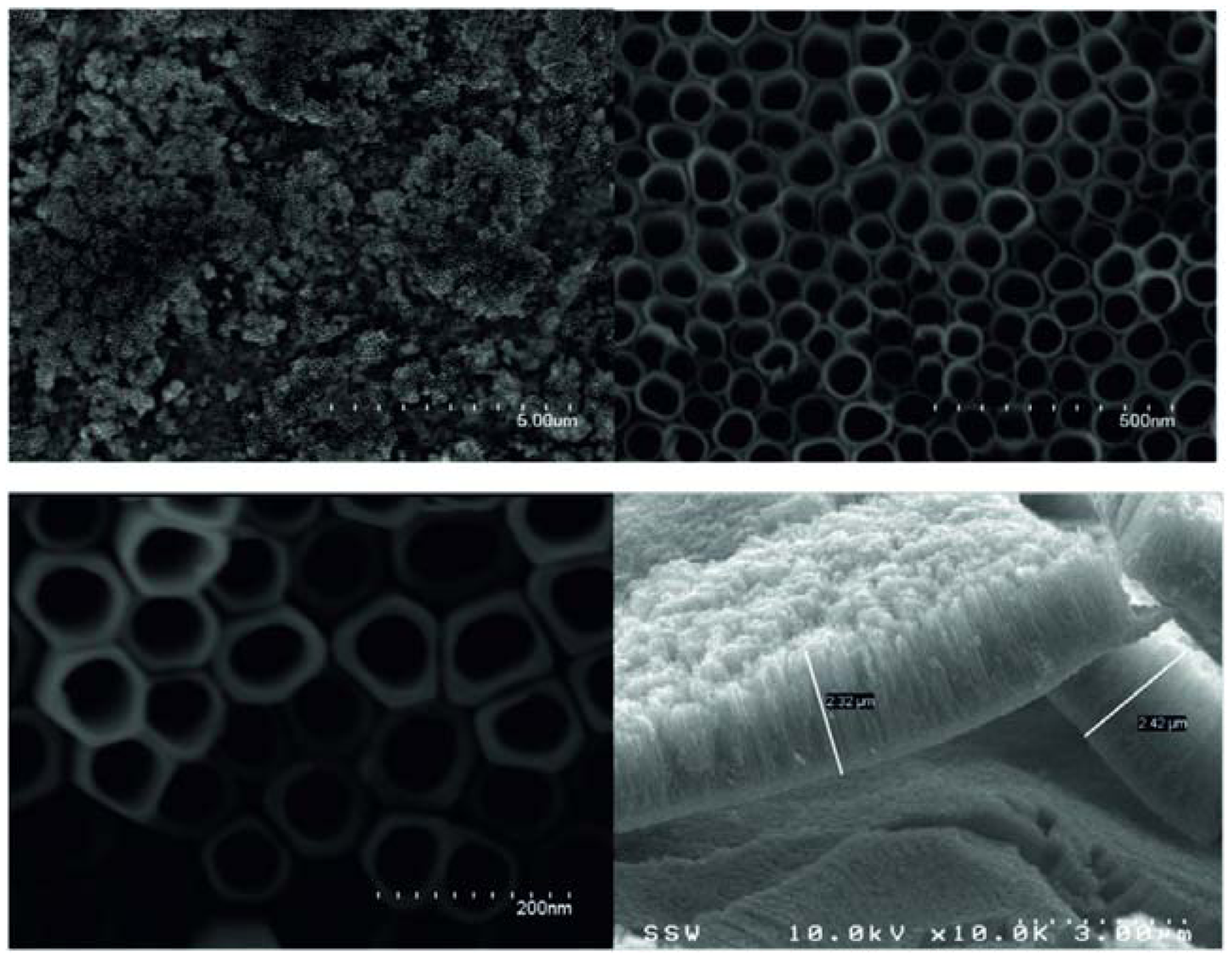
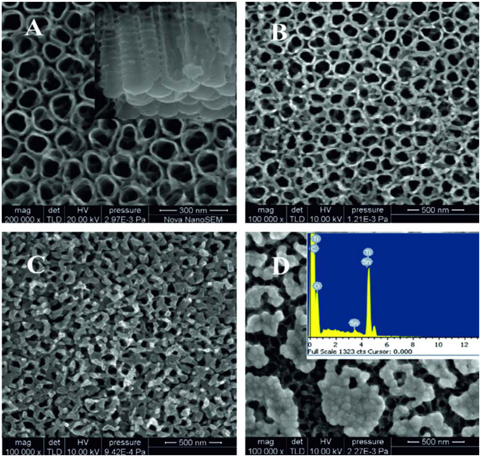
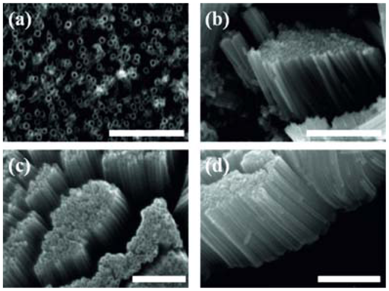
Lai et al. also reported another interesting approach for the preparation of mixed TiO2 nanotubes in [76]. Tungsten trioxide (WO3) was incorporated throughout the walls of anodized TiO2 nanotubes by a wet impregnation method. Anodized TiO2 nanotube foil was dipped into an ammonium paratungstate (APT) aqueous solution with different molarities for 1 h. Subsequently, the samples were annealed at 400 °C, which decomposed the APT into tungsten trioxide (WO3). Meng et al. modified the TiO2 nanotubes in the autoclave [61]. Initially anodized TiO2 nanotubes were annealed in a CO atmosphere at 500 °C. Then the SnO2@C-TiO2 nanotubes were prepared by hydrothermal synthesis in a Teflon-lined stainless steel autoclave. The solution in the autoclave was 0.02 M SnCl·5H2O and 0.04 M NaOH in 50 mL deionized water. The samples were rinsed with distilled water several times in order to remove the residual reactant and then dried at 60 °C. When the reaction time was increased to 7 h (Figure 13), the SnO2 particles aggregated together on the nanotubes and the pores were blocked by the undesired nucleation and growth.
The abovementioned approaches for the synthesis of doped, mixed and modified titania nanotubes have been reported recently, and they still need to be improved. The fabrication of doped and mixed TiO2 nanostructures over a wide range of concentrations requires different approaches. Depending on the type and the concentration of dopant it is possible to change its functional properties [21,47,77–79], therefore it is very important to find the more suitable method for introduction of a specific mixture in titania nanotubes.
3. Gas Sensing Properties of Titania Nanotubes
3.1. Sensing Mechanism
Deviation of stoichiometry of high gap metal oxide is responsible of the semiconducting properties [80]: cation vacancies are acceptors, producing holes and negative charged vacancies, while shallow states made up of oxygen vacancies are double n-type donors, and the electrons on the adjacent cation are easily removed and donated to the conduction band [81].
The working temperature of metal oxide gas sensors ranges between 500 and 800 K in order to keep donor oxygen vacancies ionized but fixed. The gas sensing properties of metal oxides arise from the adsorption of molecules from the gas phase on reactive surface atoms. The first step of adsorption is physisorption, which is a slightly exothermic process characterized by high coverage at low temperature and a low coverage at high temperature. Physisorbed species can be chemisorbed (ionosorbed) when the adsorbate acts as a surface state capturing an electron or a hole [82]. In fact in the simple Charge Transfer Model (CTM) [83] the physi- and chemisorbed atoms and molecules are represented by surface localized states in the semiconductor energy gap, whose occupation statistic is given by the same Fermi-Dirac distribution, with physisorption corresponding to unoccupied and chemisorption to occupied states. The appearance of surface-localized acceptor states in n-type semiconductors induces charge transfer between bulk and surface in order to establish thermal equilibrium between the two. The charge transfer results in a non-neutral region (with a non-zero electric field) in the semiconductor bulk, usually referred to as the surface space charge region (SCR) [82,84]. The process of gas detection is related to the reactions between the species to be detected and ionosorbed surface oxygen [59]. Direct adsorption is also proposed for the gaseous species -like strongly electronegative NO2 whose effect is to decrease sensor conductance. An important ubiquitous species that ionosorbs over MOX surfaces is water; the chemisorption of water onto oxide from air can be very strong, forming a “hydroxylated surface” [82]. As for signal transduction, the easiest measurable physical quantity is the sensor conductance under DC conditions. The sensor response towards a target gas concentration is defined as the (relative) change of conductance (resistance in presence of NO2 or other oxidizing species). Starting from the sensor response it is possible to derive the sensor response curve, which is the representation of the steady state output as a function of the input concentration [85].
3.2. Fabrication of Sensing Devices
Concerning the integration of titania nanotubes into chemical sensing devices several approaches have been reported in the literature. These approaches may be divided firstly considering the eventual use of a substrate for the growth of nanotubes or the direct use of titanium foils. The majority of the literature data follow the second approach, which is the easiest method; nonetheless there are several drawbacks that have to be taken into account. First of all the reliability of the chemical sensing device is strongly dependent on the stability of the electrical contacts, and furthermore the contact preparation process must be as standard as possible in order to evaluate the performances of equivalent devices and not the ones of a single device.
Metal contacts are needed in order to measure electrical properties. The first sensing devices based on titania nanotubes were prepared using an anodized titanium foil and two platinum electrodes pressed onto the nanotubes [86]. Silver paste may be used also, but lack of reproducibility is an issue. Afterwards the anodization of titanium thin film was proposed, together with a direct integration in sensing devices [87] and metallic electrodes were evaporated onto the nanotubular array.
The use of films instead of a metallic foil allows for the direct integration of nanotubes on the transducer. The choice and the proper design of the transducer affect the response of the final device. Moreover a proper choice of bonding and packaging is needed to provide a final sensor device for practical applications.
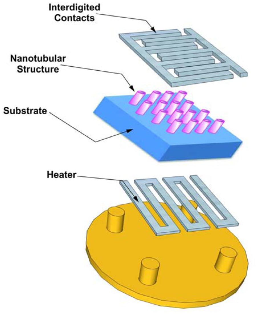
Substrates for gas sensors are usually made of alumina or silicon. When the substrate is conductive an additional layer is required to guarantee insulation of the oxide layer. A heater is needed in order to maintain the layer at the appropriate temperature (up to hundreds of degrees centigrade). Alumina is one of the best substrates thanks to its availability with different roughnesses and crystalline properties. Figure 14 describes a design of the simplest transducer, a bulk substrate with the tubular structure and the electrical contacts on the front side of the substrate and a heater on the back side. In order to reach the desired operating temperature and to keep it constant on the titania nanotubes surface, a constant voltage may be applied to the heater with a feedback circuit to keep either resistance or power consumption constant by Joule heating.
Such transducers are prepared using thin or thick film technologies, the temperature uniformity is good, but unfortunately the power consumption is quite high, in the range 320–490 mW for 300–400 °C for a 2 × 2 mm substrate [88].
The choice of the metal for the electrical contacts is another key aspect, as it can affect the sensing properties of the final device. The contact has to provide as low a sheet resistance as possible in order to minimize the voltage drops between the connections, furthermore it should be ohmic. Platinum is of widespread use for metal oxides since it produces a good ohmic contact, it does not oxidize at high temperatures, it has a low diffusivity and it is resistive to corrosive gases. Gold on the other hand diffuses quickly and may introduce unintentional doping of titanium oxide nanotubes.
As the achievement of stable and reliable titania chemical sensors is important, a particular focus has to placed on the in-depth understanding of the detection mechanism and how the changes in material resistance influence the resistance variation of the entire device. The resistance modulation may be due to a change in the inter-grain potential barrier, but also in the metal semiconductor barrier at the electrical contacts. The latter may depend on the surrounding atmosphere and furthermore there may be possible chemical interactions due to the catalytic nature of the electrode (in general platinum, gold or silver), surface species may diffuse faster to the oxide interface where it can react (spill-over effect).
The most used measurement for chemical sensors is the two probe one that cannot separate the contributions of the active layer and contact resistance to the sensing properties. Changing the metal used for the electrical contacts and connections may influence the sensing performance, therefore great attention has to be paid to the overall device and not just to the sensing layer itself. In order to distinguish the contribution of the active layer four probe array analysis either in square or in collinear configuration may be used, but this increases the difficulties in the preparation of the device, and therefore is almost never proposed.
3.3. Sensing Performances
Starting from the first paper that pointed out the feasibility of using arrays of titania nanotubes as chemical sensors [89], effort has been made in the investigation of sensing performances of titania nanotubes. The majority of the works found in literature are based on nanotube arrays. In this case, a lot of nanotubes are contacted and contribute to the measured electrical and sensing properties. The uniformity of these arrays is generally good, the dispersion in the nanotubes diameter and spacing is low (20%) [90]. Making a single nanotube-based device has intrinsic technical difficulties for the manipulation of the structure and the preparation of reliable electrical contacts on one individual nanostructure with a fabrication process controlled at the nanoscale level. Chemical sensing performances will be classified on the base of the target species, and also on the base of key parameters such as gas carrier, humidity and operating temperatures (Table 3).
When dealing with chemical sensors there are several essential factors that we have to take into account and control carefully, first of all the gas carrier used for the dispersion of the target gas, then the relative humidity and moreover the operating temperature. In the majority of the applications of chemical sensors in real environments there is humid air as a background in which the gases may be detected, therefore the measurements should be made using humid air as gas carrier instead of nitrogen or synthetic air, otherwise the results obtained are not relevant for the preparation of chemical sensors. Oxygen and water vapor play a crucial role on the semiconducting surface and completely change the sensing performances. Sensors are heated in order to activate surface reactions with gaseous species [91].
Many authors did not follow this testing procedure, therefore the comparison of the results from different groups is quite difficult. A constant flux of gaseous species at ambient pressure should be preferred to an injection of desired amount of gas through a syringe in order to study the steady state gas-surface interaction.
The first report on titania nanotube sensing has been proposed in 2003 [89] using a furnace to control the nanotubes' temperature and hydrogen gas was dispersed in nitrogen (carrier gas). An extremely high variation in the electrical resistance was registered as 100–500 ppm of hydrogen was introduced in the test chamber at temperatures ranging between 300–400 °C. This variation in the nanotubes resistance was attributed to hydrogen chemisorption, and an increase in the variation with a decreasing pore diameter was measured.
Following this first report, other articles were published on the gas-surface interactions between titania nanotubes, prepared by anodization of metallic foil, and [12,92], oxygen and SO2 using nitrogen as gas carrier. The responses of amorphous titania nanotubes arrays towards 200 ppm of oxygen at 50–100 °C is reported in [93]. Response time was relatively long, but a complete recovery of the resistance in nitrogen was registered as the nitrogen flow was restored. Zhang et al. studied the interaction with 50 ppm of SO2 as a decomposition product of SF6 with anatase titania nanotubular arrays using silver glue for electrical connection and a furnace to operate from room temperature to 400 °C. The maximum value of the relative change in resistance is 0.8 approximately, relsatively low, but with a good reproducibility when UV light was used to help the desorption of SO2 molecules absorbed on the titania surface. Nitrogen dioxide and carbon monoxide interaction was reported in [94] using Ar as gas carrier, concentrations in the range 10–100 ppm and operating temperatures of 300–500 °C.
The most interesting results for the integration of titania nanotubes into chemical sensors are the ones made for hydrogen [95], ethanol [39,72,87,95,96] ammonia [95,96] and carbon monoxide [39,95] in an air environment. Depending on the preparation technique selected, on the electrical contacts and the measurements technique, different performances have been reported. For example relatively high selectivity towards hydrogen at concentrations of 1,000 ppm with respect to ammonia, carbon monoxide and ethanol at an operating temperature of 100 °C have been reported in [95] (Figure 15). Furthermore the authors report also a good stability and repeatability, which are key aspects for the successful integration in sensing devices.
Chen and co-workers also reported good sensing performances towards hydrogen at room temperature using anodization from titanium foil, platinum or platinum/titanium contacts and the sensor was kept at room temperature [73]. The influence of the environment and electrical contacts was investigated showing a decrease in performance in the presence of oxygen and with Pt/Ti electrodes.
Reference [72] reported instead a relative variation in conductance of about 104 to 1,000 ppm of ethanol at 250 °C; electrical contacts were made with silver glue and gold wires and the gas test measurements were made using a microsyringe to insert a concentration pulse in the environment close to the titania nanotubes array. Static measurements of ethanol and ammonia at room temperature on titania nanotubular arrays prepared by anodization of metallic foil and using a stainless steel crocodile as electrode for gas tests have been reported by Perrillo et al. [96].
Reference [39] reported sensing performances of titania nanotubes arrays prepared by anodization of titanium thin film integrated directly on alumina transducers and contacted with platinum interdigitated electrodes deposited by sputtering. The result showed good sensing performances toward carbon monoxide and ethanol at 200 °C using humid synthetic air as gas carrier.
Even if the majority of the research work published concerns nanotubes arrays, there is a publication on single nanotube based devices. A single nanotube was transferred onto a silicon wafer and was integrated into a field effect transistor [97], allowing the measurement of the electrical transport characteristics (electron mobility and electron concentration) of the individual nanotube, which are interesting parameters for conductometric chemical sensors. Furthermore its sensing performances towards humidity at room temperature were studied.
Actually the main drawback of using titania for chemical sensing is its high resistivity that does not allow an easy integration in chemical sensing systems. It requires expensive equipment for the signal readout. Research efforts have been made to increase the conductance of titania in the form of thin or thick films and also in forms of nanotubes.
Concerning chemical sensor preparation, investigations have been performed on the role of niobium doping on titania nanotubes conductance and chemical sensing performances [47,98]. Reference [47] reports the achievement of Nb-doped (0.14 at%) titania nanotubes by anodization of a Nb-Ti thin film. This concentration was enough to remarkably change the sensing performances (Figure 16) and the conductance, but the latter remained at values still not compatible with standard electronics. Further work of the same authors showed that a highly conducting titania nanotube array can be achieved by a room temperature synthesis of 5% wt Nb-containing titania nanotubular arrays. Results have shown that Nb does not segregate and effectively improves titania nanotube conductance to 10−4 S while maintaining good gas sensing performances.
4. Conclusions
Electrochemical anodization is by far the more performing technique for the synthesis, doping and modification of titania nanotubes. The surface morphology and the parameters of tubular arrays depend on the type, temperature and pH of the electrolyte, as well as the anodization time and the surface of the substrate. Good alignment and high ordering of tubes is straightforward to get reproducible gas sensing properties: thanks to their highly ordered and well-aligned structures, titania nanotubes have great potential applications in metal oxide gas sensors. Besides, doped and mixed oxide titania nanotubes with improved functional properties can be obtained by the anodization method. First of all doping improves the conductivity of TiO2, mainly in the high temperature range where the material is most sensitive to gaseous species. Given the high resistivity of pure TiO2, conductivity improvement is compulsory for low cost gas sensing. Furthermore introduction of dopants greatly enhances the gas sensing performance of TiO2 nanotubes.
Acknowledgments
The research leading to these results has received funding from the Italian Ministry of Education through project FIRB “Rete Nazionale di Ricerca sulle Nanoscienze ItalNanoNet” (Protocollo: RBPR05JH2P, 2009-2013), Italian MIUR through the project FIRB RBAP115AYN “Oxides at the nanoscale: multifunctionality and applications”, European Communities 7th Framework Programme under grant agreement NMP3-LA-2010-246334, ORAMA and Region Lombardia (Italy) through the project “Xnano”.
Conflicts of Interest
The authors declare no conflict of interest.
References
- Lee, J.; Orilall, M.C.; Warren, S.C.; Kamperman, M.; Disalvo, F.J.; Wiesner, U. Direct access to thermally stable and highly crystalline mesoporous transition-metal oxides with uniform pores. Nat. Mater. 2008, 7, 222–228. [Google Scholar]
- Bolink, H.J.; Coronado, E.; Orozco, J.; Sessolo, M. Efficient polymer light-emitting diode using air-stable metal oxides as electrodes. Adv. Mater. 2009, 21, 79–82. [Google Scholar]
- Vallejos, S.; Khatko, V.; Calderer, J.; Gracia, I.; Cane, C.; Llobet, E.; Correig, X. Micro-machined WO3-based sensors selective to oxidizing gases. Sens. Actuators B Chem. 2008, 132, 209–215. [Google Scholar]
- Alessandri, I.; Comini, E.; Bontempi, E.; Faglia, G.; Depero, L.E.; Sberveglieri, G. Cr-inserted TiO2 thin films for chemical gas sensors. Sens. Actuators B Chem. 2007, 128, 312–319. [Google Scholar]
- Ponce, M.A.; Parra, R.; Savu, R.; Joanni, E.; Bueno, P.R.; Cilense, M.; Varela, J.A.; Castro, M.S. Impedance spectroscopy analysis of TiO2 thin film gas sensors obtained from water-based anatase colloids. Sens. Actuators B Chem. 2009, 139, 447–452. [Google Scholar]
- Tian, W.C.; Ho, Y.H.; Chen, C.H.; Kuo, C.Y. Sensing performance of precisely ordered TiO2 nanowire gas sensors fabricated by electron-beam lithography. Sensors 2013, 13, 865–874. [Google Scholar]
- Kim, I.D.; Rothschild, A.; Yang, D.J.; Tuller, H.L. Macroporous TiO2 thin film gas sensors obtained using colloidal templates. Sens. Actuators B Chem. 2008, 130, 9–13. [Google Scholar]
- Paulose, M.; Varghese, O.K.; Mor, G.K.; Grimes, C.A.; Ong, K.G. Unprecedented ultra-high hydrogen gas sensitivity in undoped titania nanotubes. Nanotechnology 2006, 17, 398–402. [Google Scholar]
- Ha, T.J.; Hong, M.H.; Park, C.S.; Park, H.H. Gas sensing properties of ordered mesoporous TiO2 film enhanced by thermal shock induced cracking. Sens. Actuators B Chem. 2013, 181, 874–879. [Google Scholar]
- Zhang, X.X.; Zhang, J.B.; Jia, Y.C.; Xiao, P.; Tang, J. TiO2 nanotube array sensor for detecting the SF6 decomposition product SO2. Sensors 2012, 12, 3302–3313. [Google Scholar]
- Varghese, O.K.; Gong, D.W.; Paulose, M.; Ong, K.G.; Grimes, C.A. Hydrogen sensing using titania nanotubes. Sens. Actuators B Chem. 2003, 93, 338–344. [Google Scholar]
- Sennik, E.; Colak, Z.; Kilinc, N.; Ozturk, Z.Z. Synthesis of highly-ordered TiO2 nanotubes for a hydrogen sensor. Int. J. Hydr. Energy 2010, 35, 4420–4427. [Google Scholar]
- Charanpahari, A.; Umare, S.S.; Sasikala, R. Effect of Ce, N and S multi-doping on the photocatalytic activity of TiO2. Appl. Surf. Sci. 2013, 282, 408–414. [Google Scholar]
- Horie, Y.; Watanabe, T.; Deguchi, M.; Asakura, D.; Nomiyama, T. Enhancement of carrier mobility by electrospun nanofibers of Nb-doped TiO2 in dye sensitized solar cells. Electrochim. Acta. 2013, 105, 394–402. [Google Scholar]
- Ok, K.C.; Park, Y.; Chung, K.B.; Park, J.S. The effect of Nb doping on the performance and stability of TiOx devices. J. Phys. D Appl. Phys. 2013, 46, 295102. [Google Scholar]
- Song, K.; Han, X.; Shao, G. Electronic properties of rutile TiO2 doped with 4d transition metals: First-principles study. J. Alloys Comp. 2013, 551, 118–124. [Google Scholar]
- Neville, E.M.; MacElroy, J.M.D.; Thampi, K.R.; Sullivan, J.A. Visible light active C-doped titanate nanotubes prepared via alkaline hydrothermal treatment of C-doped nanoparticulate TiO2: Photo-electrochemical and photocatalytic properties. J. Photochem. Photobiol. A Chem. 2013, 267, 17–24. [Google Scholar]
- Guo, S.; Han, S.; Haifeng, M.; Zeng, C.; Sun, Y.; Chi, B.; Pu, J.; Li, J. Synthesis of phosphorus-doped titania with mesoporous structure and excellent photocatalytic activity. Mater. Res. Bull. 2013, 48, 3032–3036. [Google Scholar]
- Gao, Y.; Thevuthasan, S.; McCready, D.E.; Engelhard, M. MOCVD growth and structure of Nb- and V-doped TiO2 films on sapphire. J. Cryst. Grow. 2000, 212, 178–190. [Google Scholar]
- Santangelo, S.; Faggio, G.; Messina, G.; Fazio, E.; Neri, F.; Neri, G. On the hydrogen sensing mechanism of Pt/TiO2/CNTs based devices. Sens. Actuators B: Chem. 2013, 178, 473–484. [Google Scholar]
- Moon, J.; Park, J.A.; Lee, S.J.; Zyung, T.; Kim, I.D. Pd-doped TiO2 nanofiber networks for gas sensor applications. Sens. Actuators B: Chem. 2010, 149, 301–305. [Google Scholar]
- Carotta, M.C.; Ferroni, M.; Gnani, D.; Guidi, V.; Merli, M.; Martinelli, G.; Casale, M.C.; Notaro, M. Nanostructured pure and Nb-doped TiO2 as thick film gas sensors for environmental monitoring. Sens. Actuators B Chem. 1999, 58, 310–317. [Google Scholar]
- Benkara, S.; Zerkout, S.; Ghamri, H. Synthesis of SN doped ZnO/TiO2 nanocomposite film and their application to H2 gas sensing properties. Mater. Sci. Semicond. Proc. 2013, 16, 1271–1279. [Google Scholar]
- Han, Z.; Wang, J.; Liao, L.; Pan, H.; Shen, S.; Chen, J. Phosphorus doped TiO2 as oxygen sensor with low operating temperature and sensing mechanism. Appl. Surf. Sci. 2013, 273, 349–356. [Google Scholar]
- Ruggieri, F.; Di Camillo, D.; Lozzi, L.; Santucci, S.; De Marcellis, A.; Ferri, G.; Giancaterini, L.; Cantalini, C. Preparation of nitrogen doped TiO2 nanofibers by near field electrospinning (NFES) technique for NO2 sensing. Sens. Actuators B Chem. 2013, 179, 107–113. [Google Scholar]
- Patil, L.A.; Suryawanshi, D.N.; Pathan, I.G.; Patil, D.M. Nickel doped spray pyrolyzed nanostructured TiO2 thin films for LPG gas sensing. Sens. Actuators B Chem. 2013, 176, 514–521. [Google Scholar]
- Zeng, W.; Liu, T.; Wang, Z. Impact of Nb doping on gas-sensing performance of TiO2thick-film sensors. Sens. Actuators B Chem. 2012, 166–167, 141–149. [Google Scholar]
- Sato, Y.; Akizuki, H.; Kamiyama, T.; Shigesato, Y. Transparent conductive Nb-doped TiO2 films deposited by direct-current magnetron sputtering using a TiO2-x target. Thin Solid Films 2008, 516, 5758–5762. [Google Scholar]
- Körner, W.; Elsässer, C. Density functional theory study of dopants in polycrystalline TiO2. Phys. Rev. B. 2011, 83, 205315. [Google Scholar]
- Arbiol, J.; Cerda, J.; Dezanneau, G.; Cirera, A.; Peiro, F.; Cornet, A.; Morante, J.R. Effects of Nb doping on the TiO2 anatase-to-rutile phase transition. J. Appl. Phys. 2002, 92, 853–861. [Google Scholar]
- Tang, H.; Prasad, K.; Sanjines, R.; Levy, F. TiO2 anatase thin-films as gas sensors. Sens. Actuators B Chem. 1995, 26, 71–75. [Google Scholar]
- Sclafani, A.; Herrmann, J.M. Comparison of the photoelectronic and photocatalytic activities of various anatase and rutile forms of titania in pure liquid organic phases and in aqueous solutions. J. Phys. Chem. 1996, 100, 13655–13661. [Google Scholar]
- Li, S.-C.; Diebold, U. Reactivity of TiO2 rutile and anatase surfaces toward nitroaromatics. J. Am. Chem. Soc. 2009, 132, 64–66. [Google Scholar]
- Su, R.; Bechstein, R.; Sø, L.; Vang, R.T.; Sillassen, M.; Esbjörnsson, B.; Palmqvist, A.; Besenbacher, F. How the anatase-to-rutile ratio influences the photoreactivity of TiO2. J. Phys. Chem. C. 2011, 115, 24287–24292. [Google Scholar]
- Hoyer, P. Formation of a titanium dioxide nanotube array. Langmuir 1996, 12, 1411–1413. [Google Scholar]
- Gong, D.; Grimes, C.A.; Varghese, O.K.; Hu, W.C.; Singh, R.S.; Chen, Z.; Dickey, E.C. Titanium oxide nanotube arrays prepared by anodic oxidation. J. Mater. Res. 2001, 16, 3331–3334. [Google Scholar]
- Beranek, R.; Hildebrand, H.; Schmuki, P. Self-organized porous titanium oxide prepared in H2SO4/HF electrolytes. Electrochem. Solid-State Lett. 2003, 6, B12–B14. [Google Scholar]
- Lai, Y.; Zhuang, H.; Sun, L.; Chen, Z.; Lin, C. Self-organized TiO2 nanotubes in mixed organic-inorganic electrolytes and their photoelectrochemical performance. Electrochim. Acta. 2009, 54, 6536–6542. [Google Scholar]
- Galstyan, V.; Vomiero, A.; Comini, E.; Faglia, G.; Sberveglieri, G. TiO2 nanotubular and nanoporous arrays by electrochemical anodization on different substrates. Rsc Adv. 2011, 1, 1038–1044. [Google Scholar]
- Foong, T.R.B.; Shen, Y.D.; Hu, X.; Sellinger, A. Template-directed liquid ald growth of TiO2 nanotube arrays: Properties and potential in photovoltaic devices. Adv. Funct. Mater. 2010, 20, 1390–1396. [Google Scholar]
- Huang, Y.J.; Pandraud, G.; Sarro, P.M. The atomic layer deposition array defined by etch-back technique: A new method to fabricate TiO2 nanopillars, nanotubes and nanochannel arrays. Nanotechnology 2012, 23, 485306. [Google Scholar]
- Chang, Y-H.; Liu, C.-M.; Chen, C.; Cheng, H.-E. The heterojunction effects of TiO2 nanotubes fabricated by atomic layer deposition on photocarrier transportation direction. Nanos. Res. Lett. 2012, 7, 1–7. [Google Scholar]
- Suzuki, Y.; Yoshikawa, S. Synthesis and thermal analyses of TiO2-derived nanotubes prepared by the hydrothermal method. J. Mater. Res. 2004, 19, 982–985. [Google Scholar]
- Choi, M.G.; Lee, Y.G.; Song, S.W.; Kim, K.M. Lithium-ion battery anode properties of TiO2 nanotubes prepared by the hydrothermal synthesis of mixed (anatase and rutile) particles. Electrochim. Acta. 2010, 55, 5975–5983. [Google Scholar]
- Zhao, P.-J.; Wu, R.; Hou, J.; Chang, A.-m.; Guan, F.; Zhang, B. One-step hydrothermal synthesis and visible-light photocatalytic activity of ultrafine Cu-nanodot-modified TiO2 nanotubes. Acta Phys.-Chim. Sin. 2012, 28, 1971–1977. [Google Scholar]
- Galstyan, V.; Comini, E.; Vomiero, A.; Ponzoni, A.; Concina, I.; Brisotto, M.; Bontempi, E.; Faglia, G.; Sberveglieri, G. Fabrication of pure and Nb-TiO2 nanotubes and their functional properties. J. Alloys Comp. 2012, 536, S488–S490. [Google Scholar]
- Galstyan, V.; Comini, E.; Faglia, G.; Vomiero, A.; Borgese, L.; Bontempi, E.; Sberveglieri, G. Fabrication and investigation of gas sensing properties of Nb-doped TiO2nanotubular arrays. Nanotechnology 2012, 23. [Google Scholar] [CrossRef]
- Zwilling, V.; Darque-Ceretti, E. Characterization of porous and compact oxide films on titanium and Ti-6A1-4V. Caracterisation d'oxydes anodiques poreux et compacts de titane et de Ta6V 1997, 22, 481–493. [Google Scholar]
- Zwilling, V.; Darque-Ceretti, E.; Boutry-Forveille, A.; David, D.; Perrin, M.Y.; Aucouturier, M. Structure and physicochemistry of anodic oxide films on titanium and Ta6V alloy. Surf. Interf. Anal. 1999, 27, 629–637. [Google Scholar]
- Sreekantan, S.; Saharudin, K.A.; Lockman, Z.; Tzu, T.W. Fast-rate formation of TiO2 nanotube arrays in an organic bath and their applications in photocatalysis. Nanotechnology 2010, 21, 365603. [Google Scholar]
- Wang, M.; Liu, Y.; Yang, H. A unified thermodynamic theory for the formation of anodized metal oxide structures. Electrochim. Acta. 2012, 62, 424–432. [Google Scholar]
- Macák, J.M.; Tsuchiya, H.; Schmuki, P. High-aspect-ratio TiO2 nanotubes by anodization of titanium. Angew. Chem. Int. Ed. 2005, 44, 2100–2102. [Google Scholar]
- Varghese, O.K.; Paulose, M.; Grimes, C.A. Long vertically aligned titania nanotubes on transparent conducting oxide for highly efficient solar cells. Nat. Nanotechnol 2009, 4, 592–597. [Google Scholar]
- Wang, J.; Lin, Z. Anodic formation of ordered TiO2 nanotube arrays: Effects of electrolyte temperature and anodization potential. J. Phys. Chem. C. 2009, 113, 4026–4030. [Google Scholar]
- Zhang, L.; Han, Y. Effect of nanostructured titanium on anodization growth of self-organized TiO2 nanotubes. Nanotechnology 2010, 21, 055602. [Google Scholar]
- Regonini, D.; Jaroenworaluck, A.; Stevens, R.; Bowen, C.R. Effect of heat treatment on the properties and structure of TiO2 nanotubes: Phase composition and chemical composition. Surf. Interf. Anal. 2010, 42, 139–144. [Google Scholar]
- Yamazoe, N.; Shimanoe, K. Roles of shape and size of component crystals in semiconductor gas sensors. J. Electrochem. Soc. 2008, 155, J85–J92. [Google Scholar]
- Yamazoe, N.; Shimanoe, K. Roles of shape and size of component crystals in semiconductor gas sensors. J. Electrochem. Soc. 2008, 155, J93–J98. [Google Scholar]
- Barsan, N.; Weimar, U. Conduction model of metal oxide gas sensors. J. Electroceram 2001, 7, 143–167. [Google Scholar]
- Ghicov, A.; Schmidt, B.; Kunze, J.; Schmuki, P. Photoresponse in the visible range from Cr doped TiO2 nanotubes. Chem. Phys. Lett. 2007, 433, 323–326. [Google Scholar]
- Meng, X.Q.; Yao, J.Y.; Liu, F.L.; He, H.C.; Zhou, M.; Xiao, P.; Zhang, Y.H. Preparation of SnO2@C-doping TiO2 nanotube arrays and its electrochemical and photoelectrochemical properties. J. Alloys Comp. 2013, 552, 392–397. [Google Scholar]
- Isimjan, T.T.; El Ruby, A.; Rohani, S.; Ray, A.K. The fabrication of highly ordered and visible-light-responsive Fe-C-N-codoped TiO2 nanotubes. Nanotechnology 2010, 21, 055706. [Google Scholar]
- Yuan, B.; Wang, Y.; Bian, H.; Shen, T.; Wu, Y.; Chen, Z. Nitrogen doped TiO2 nanotube arrays with high photoelectrochemical activity for photocatalytic applications. Appl. Surf. Sci. 2013, 280, 523–529. [Google Scholar]
- Li, D.; Zhang, Y.; Zhang, Y.; Zhou, X.; Guo, S. Fabrication of bidirectionally doped β-Bi2O3/TiO2-NTs with enhanced photocatalysis under visible light irradiation. J. Hazard. Mater. 2013, 258–259, 42–49. [Google Scholar]
- Zhang, X.; Tang, Y.; Li, Y.; Wang, Y.; Liu, X.; Liu, C.; Luo, S. Reduced graphene oxide and PbS nanoparticles co-modified TiO2 nanotube arrays as a recyclable and stable photocatalyst for efficient degradation of pentachlorophenol. Appl. Catal. A General 2013, 457, 78–84. [Google Scholar]
- Liu, C.; Teng, Y.; Liu, R.; Luo, S.; Tang, Y.; Chen, L.; Cai, Q. Fabrication of graphene films on TiO2 nanotube arrays for photocatalytic application. Carbon 2011, 49, 5312–5320. [Google Scholar]
- Ding, D.Y.; Ning, C.Q.; Huang, L.; Jin, F.C.; Hao, Y.Q.; Bai, S.; Li, Y.; Li, M.; Mao, D.L. Anodic fabrication and bioactivity of Nb-doped TiO2 nanotubes. Nanotechnology 2009, 20, 305103. [Google Scholar]
- Hao, Y.Q.; Li, S.J.; Hao, Y.L.; Zhao, Y.K.; Ai, H.J. Effect of nanotube diameters on bioactivity of a multifunctional titanium alloy. Appl. Surf. Sci. 2013, 268, 44–51. [Google Scholar]
- Moon, S.H.; Lee, S.J.; Park, I.S.; Lee, M.H.; Soh, Y.J.; Bae, T.S.; Kim, H.S. Bioactivity of Ti-6Al-4V alloy implants treated with ibandronate after the formation of the nanotube TiO2 layer. J. Biomed. Mater. Res. Part B Appl. Biomater. 2012, 100B, 2053–2059. [Google Scholar]
- Roguska, A.; Belcarz, A.; Piersiak, T.; Pisarek, M.; Ginalska, G.; Lewandowska, M. Evaluation of the antibacterial activity of Ag-loaded TiO2nanotubes. Eur. J. Inorg. Chem. 2012, 5199–5206. [Google Scholar]
- Hang, R.; Huang, X.; Tian, L.; He, Z.; Tang, B. Preparation, characterization, corrosion behavior and bioactivity of Ni2O3-doped TiO2 nanotubes on NiTi alloy. Electrochim. Acta. 2012, 70, 382–393. [Google Scholar]
- Kwon, Y.; Kim, H.; Lee, S.; Chin, I.J.; Seong, T.Y.; Lee, W.I.; Lee, C. Enhanced ethanol sensing properties of TiO2 nanotube sensors. Sens. Actuators B Chem. 2012, 173, 441–446. [Google Scholar]
- Chen, K.S.; Xie, K.; Feng, X.R.; Wang, S.F.; Hu, R.; Gu, H.S.; Li, Y. An excellent room-temperature hydrogen sensor based on titania nanotube-arrays. Int. J. Hydr. Energy 2012, 37, 13602–13609. [Google Scholar]
- Liu, R.; Yang, W.-D.; Qiang, L.-S.; Liu, H.-Y. Conveniently fabricated heterojunction ZnO/TiO2 electrodes using TiO2 nanotube arrays for dye-sensitized solar cells. J. Power Sour. 2012, 220, 153–159. [Google Scholar]
- Das, C.; Paramasivam, I.; Liu, N.; Schmuki, P. Photoelectrochemical and photocatalytic activity of tungsten doped TiO2 nanotube layers in the near visible region. Electrochim. Acta. 2011, 56, 10557–10561. [Google Scholar]
- Lai, C.W.; Sreekantan, S. Incorporation of WO3 species into TiO2 nanotubes via wet impregnation and their water-splitting performance. Electrochim. Acta 2013, 87, 294–302. [Google Scholar]
- Choi, Y.J.; Seeley, Z.; Bandyopadhyay, A.; Bose, S.; Akbar, S.A. Aluminum-doped TiO2 nano-powders for gas sensors. Sens. Actuators B Chem. 2007, 124, 111–117. [Google Scholar]
- Zeng, W.; Liu, T.M.; Wang, Z.C. Impact of Nb doping on gas-sensing performance of TiO2 thick-film sensors. Sens. Actuators B Chem. 2012, 166, 141–149. [Google Scholar]
- Singh, S.; Kaur, H.; Singh, V.N.; Jain, K.; Senguttuvan, T.D. Highly sensitive and pulse-like response toward ethanol of Nb doped TiO2 nanorods based gas sensors. Sens. Actuators B Chem 2012, 171, 899–906. [Google Scholar]
- Tsuda, N.; Nasu, K.; Fujimori, A.; Siratori, K. Electronic Conduction in Oxides, 2 ed; Springer: Berlin, Germany, 2000; p. 369. [Google Scholar]
- Samson, S.; Fonstad, C.G. Defect structure and electronic donor levels in stannic oxide crystals. J. Appl. Phys. 1973, 44, 4618–4621. [Google Scholar]
- Madou, M.J.; Morrison, S.R. Chemical Sensing with Solid State Devices; Academic Press: Boston, MA, USA, 1989. [Google Scholar]
- Kronik, L.; Shapira, Y. Surface photovoltage phenomena: Theory, experiment, and applications. Surf. Sci. Rep. 1999, 37, 1–206. [Google Scholar]
- Morrison, S.R. The Chemical Physics of Surfaces; Plenum Press: New York, NY, USA, 1977. [Google Scholar]
- D'Amico, A.; Di Natale, C. A contribution on some basic definitions of sensors properties. IEEE Sens. J. 2001, 1, 183–190. [Google Scholar]
- Grimes, C.A.; Ong, K.G.; Varghese, O.K.; Yang, X.P.; Mor, G.; Paulose, M.; Dickey, E.C.; Ruan, C.M.; Pishko, M.V.; Kendig, J.W.; et al. A sentinel sensor network for hydrogen sensing. Sensors 2003, 3, 69–82. [Google Scholar]
- Kilinc, N.; Sennik, E.; Ozturk, Z.Z. Fabrication of TiO2 nanotubes by anodization of Ti thin films for VOC sensing. Thin Solid Films 2011, 520, 953–958. [Google Scholar]
- Comini, E.; Faglia, G.; Sberveglieri, G. Electrical-Based Gas Sensing. In Solid State Gas Sensing; Springer: New York, NY, USA, 2009. [Google Scholar]
- Varghese, O.K.; Gong, D.W.; Paulose, M.; Ong, K.G.; Dickey, E.C.; Grimes, C.A. Extreme changes in the electrical resistance of titania nanotubes with hydrogen exposure. Adv. Mater. 2003, 15, 624–627. [Google Scholar]
- Kaneco, S.; Chen, Y.; Westerhoff, P.; Crittenden, J.C. Fabrication of uniform size titanium oxide nanotubes: Impact of current density and solution conditions. Scripta Mater. 2007, 56, 373–376. [Google Scholar]
- Korotchenkov, G.S. Chemical Sensors: Comprehensive Sensors Technologies; Momentum Press: New York, NY, USA, 2011. [Google Scholar]
- Asl, S.K.; Alavi, B.; Ahmadi, S. The effect of highly ordered titania nanotube structures on hydrogen gas detection. Surf. Interf. Anal. 2012, 44, 1051–1053. [Google Scholar]
- Lu, H.F.; Li, F.; Liu, G.; Chen, Z.G.; Wang, D.W.; Fang, H.T.; Lu, G.Q.; Jiang, Z.H.; Cheng, H.M. Amorphous TiO2 nanotube arrays for low-temperature oxygen sensors. Nanotechnology 2008, 19, 405504. [Google Scholar]
- Gonullu, Y.; Rodriguez, G.C.M.; Saruhan, B.; Urgen, M. Improvement of gas sensing performance of TiO2 towards NO2 by nano-tubular structuring. Sens. Actuators B Chem. 2012, 169, 151–160. [Google Scholar]
- Lee, J.; Kim, D.H.; Hong, S.H.; Jho, J.Y. A hydrogen gas sensor employing vertically aligned TiO2 nanotube arrays prepared by template-assisted method. Sens. Actuators B Chem. 2011, 160, 1494–1498. [Google Scholar]
- Perillo, P.M.; Rodriguez, D.F. The gas sensing properties at room temperature of TiO2 nanotubes by anodization. Sens. Actuators B Chem. 2012, 171, 639–643. [Google Scholar]
- Liang, F.X.; Luo, L.B.; Tsang, C.K.; Zheng, L.X.; Cheng, H.; Li, Y.Y. TiO2 nanotube-based field effect transistors and their application as humidity sensors. Mater. Res. Bull. 2012, 47, 54–58. [Google Scholar]
- Liu, H.G.; Ding, D.Y.; Ning, C.Q.; Li, Z.H. Wide-range hydrogen sensing with Nb-doped TiO2 nanotubes. Nanotechnology 2012, 23, 015502. [Google Scholar]


| References | Preparation Method | Growth Temperature (°C) | Crystal Structure | Possibility of Size Control | Template-Assisted Technique | Distribution over the Substrate | Starting Material |
|---|---|---|---|---|---|---|---|
| [36–39,47] | Electro-chemical anodization | Room temperature | Amorphous | Yes | No | Well-ordered and vertically-aligned | Metallic Ti |
| [40,42] | ALD | 90–400 | Amorphous/ crystalline | Yes | Yes | Well-ordered and vertically-aligned | Precursor solution |
| [17,44,45] | Hydrothermal synthesis | 300–450 | Titanate, anatase | Yes | No | Chaotic distribution (powder) | TiO2 crystalline nanoparticulate powder, precursor solution |
| 10 V (30 nm pore size) | |||
|---|---|---|---|
| Length | Log(S) | Log(S) | |
| pH | (nm) | no Pd | with Pd |
| 1.1 | 350 | 7.2 | 7.3 |
| 3.0 | 730 | 8.0 | 8.7 |
| 4.0 | 990 | 8.7 | 8.3 |
| 4.5 | 1400 | 8.0 | 8.3 |
| 5.0 | 2000 | – | – |
| Reference | Preparation | Contacts | Gas Carrier | Measurement | Gas |
|---|---|---|---|---|---|
| [89] | Ti foil anodization | Pt | N2 | Dynamic flow | H2, CO, NH3 |
| [93] | Ti foil anodization | Pt | N2 | Dynamic flow | O2 |
| [12] | Ti foil anodization | Pt | N2 | Dynamic flow | H2 |
| [92] | Ti foil anodization | Au + Ag | N2 | Dynamic flow | H2 |
| [10] | Ti foil anodization | Ag | N2 | Dynamic flow | SO2 |
| [94] | Ti foil anodization | Pt | Ar | Dynamic flow | NO2, CO |
| [96] | Ti foil anodization | Stainless steel | Air | Static | Ethanol, NH3 |
| [73] | Ti foil anodization | Pt | Ar | Static | H2 |
| [72] | Ti foil anodization | Ag+Au | Air | Static | ethanol |
| [87] | Ti film on glass | Au | Air | Static | Volatile organic compounds |
| [95] | ALD | Pt | Air | Dynamic flow | H2, CO, ethanol, NH3 |
| [98] | Ti35Nb foil anodization | Pt + Ag + Cu | Air, N2 | Dynamic flow | H2 |
| [39] | Ti film on alumina anodization | Pt | Air | Dynamic flow | CO, ethanol |
| [47] | Ti/Nb film on alumina anodization | Pt | Air | Dynamic flow | CO, NO2, H2, ethanol, acetone |
© 2013 by the authors; licensee MDPI, Basel, Switzerland. This article is an open access article distributed under the terms and conditions of the Creative Commons Attribution license (http://creativecommons.org/licenses/by/3.0/).
Share and Cite
Galstyan, V.; Comini, E.; Faglia, G.; Sberveglieri, G. TiO2 Nanotubes: Recent Advances in Synthesis and Gas Sensing Properties. Sensors 2013, 13, 14813-14838. https://doi.org/10.3390/s131114813
Galstyan V, Comini E, Faglia G, Sberveglieri G. TiO2 Nanotubes: Recent Advances in Synthesis and Gas Sensing Properties. Sensors. 2013; 13(11):14813-14838. https://doi.org/10.3390/s131114813
Chicago/Turabian StyleGalstyan, Vardan, Elisabetta Comini, Guido Faglia, and Giorgio Sberveglieri. 2013. "TiO2 Nanotubes: Recent Advances in Synthesis and Gas Sensing Properties" Sensors 13, no. 11: 14813-14838. https://doi.org/10.3390/s131114813