<?xml version="1.0" encoding="UTF-8"?>
<!DOCTYPE article PUBLIC "-//NLM//DTD Journal Publishing DTD v2.3 20070202//EN" "journalpublishing.dtd">
<article xmlns:mml="http://www.w3.org/1998/Math/MathML" xmlns:xlink="http://www.w3.org/1999/xlink" xml:lang="en" article-type="review-article">
<front>
<journal-meta>
<journal-id journal-id-type="nlm-ta">Sensors</journal-id>
<journal-title>Sensors</journal-title>
<issn pub-type="epub">1424-8220</issn>
<publisher>
<publisher-name>Molecular Diversity Preservation International (MDPI)</publisher-name></publisher></journal-meta>
<article-meta>
<article-id pub-id-type="doi">10.3390/s120811406</article-id>
<article-id pub-id-type="publisher-id">sensors-12-11406</article-id>
<article-categories>
<subj-group>
<subject>Review</subject></subj-group></article-categories>
<title-group>
<article-title>Development and Application of Integrated Optical Sensors for Intense E-Field Measurement</article-title></title-group>
<contrib-group>
<contrib contrib-type="author">
<name><surname>Zeng</surname><given-names>Rong</given-names></name><xref ref-type="corresp" rid="c1-sensors-12-11406"><sup>*</sup></xref></contrib>
<contrib contrib-type="author">
<name><surname>Wang</surname><given-names>Bo</given-names></name></contrib>
<contrib contrib-type="author">
<name><surname>Niu</surname><given-names>Ben</given-names></name></contrib>
<contrib contrib-type="author">
<name><surname>Yu</surname><given-names>Zhanqing</given-names></name></contrib>
<aff id="af1-sensors-12-11406">State Key Lab of Power Systems, Department of Electrical Engineering, Tsinghua University, Beijing 100084, China; E-Mails: <email>wang-b04@mails.tsinghua.edu.cn</email> (B.W.); <email>niuben@tsinghua.edu.cn</email> (B.N.); <email>yzq@tsinghua.edu.cn</email> (Z.Y.)</aff></contrib-group>
<author-notes>
<corresp id="c1-sensors-12-11406">
<label>*</label>Author to whom correspondence should be addressed; E-Mail: <email>zengrong@tsinghua.edu.cn</email>; Tel.: +86-10-6278-9626; Fax: +86-10-6278-3057.</corresp></author-notes>
<pub-date pub-type="collection">
<year>2012</year></pub-date>
<pub-date pub-type="epub">
<day>21</day>
<month>08</month>
<year>2012</year></pub-date>
<volume>12</volume>
<issue>8</issue>
<fpage>11406</fpage>
<lpage>11434</lpage>
<history>
<date date-type="received">
<day>22</day>
<month>06</month>
<year>2012</year></date>
<date date-type="rev-recd">
<day>25</day>
<month>07</month>
<year>2012</year></date>
<date date-type="accepted">
<day>31</day>
<month>07</month>
<year>2012</year></date></history>
<permissions>
<copyright-statement>© 2012 by the authors; licensee MDPI, Basel, Switzerland.</copyright-statement>
<copyright-year>2012</copyright-year>
<license>
<p>This article is an open access article distributed under the terms and conditions of the Creative Commons Attribution license (http://creativecommons.org/licenses/by/3.0/).</p></license></permissions>
<abstract>
<p>The measurement of intense E-fields is a fundamental need in various research areas. Integrated optical E-field sensors (IOESs) have important advantages and are potentially suitable for intense E-field detection. This paper comprehensively reviews the development and applications of several types of IOESs over the last 30 years, including the Mach-Zehnder interferometer (MZI), coupler interferometer (CI) and common path interferometer (CPI). The features of the different types of IOESs are compared, showing that the MZI has higher sensitivity, the CI has a controllable optical bias, and the CPI has better temperature stability. More specifically, the improvement work of applying IOESs to intense E-field measurement is illustrated. Finally, typical uses of IOESs in the measurement of intense E-fields are demonstrated, including application areas such as E-fields with different frequency ranges in high-voltage engineering, simulated nuclear electromagnetic pulse in high-power electromagnetic pulses, and ion-accelerating field in high-energy physics.</p></abstract>
<kwd-group>
<kwd>electric field</kwd>
<kwd>E-field sensor</kwd>
<kwd>Pockels effect</kwd>
<kwd>integrated optics</kwd></kwd-group></article-meta></front>
<body>
<sec sec-type="intro">
<label>1.</label>
<title>Introduction</title>
<sec>
<label>1.1.</label>
<title>The Demand for and Characteristics of Intense E-Field Measurement</title>
<p>
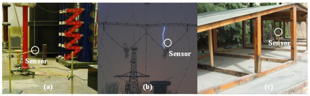
The E-field is a fundamental physical parameter that describes electromagnetic phenomena, and measurement of these phenomena is a basic tool for research in various fields of science and technology. First, in high-voltage engineering studies, various phenomena and problems are attributed to the presence of an E-field, e.g., corona discharge, partial discharge, gap breakdown, and the electromagnetic environment. The acquisition of a direct current (DC) field distribution is important in the optimization of a high voltage direct current converter station [<xref ref-type="bibr" rid="b1-sensors-12-11406">1</xref>]. An alternating current (AC) power frequency E-field measurement near the surface of an overhead line is essential to the study of electromagnetic environmental problems [<xref ref-type="bibr" rid="b2-sensors-12-11406">2</xref>]. Microsecond-order transient E-field detection is necessary for understanding the physical process of long air gap discharge and lightning [<xref ref-type="bibr" rid="b3-sensors-12-11406">3</xref>], shown in <xref ref-type="fig" rid="f1-sensors-12-11406">Figure 1(a) and Figure 1(b)</xref>. Nanosecond-order transient E-field measurement is significant for the investigation of very fast transient overvoltage (VFTO) in a gas insulation substation (GIS) [<xref ref-type="bibr" rid="b4-sensors-12-11406">4</xref>].</p>
<p>Second, high-power electromagnetic pulses (HPEMs) include nuclear electromagnetic pulses (NEMPs), electro-static discharges and high-power microwaves [<xref ref-type="bibr" rid="b5-sensors-12-11406">5</xref>]. HPEMs have caused severe damage to life and property in the civil and military domains [<xref ref-type="bibr" rid="b6-sensors-12-11406">6</xref>]. The amplitude and frequency characteristics of the HPEM field should be studied to evaluate the hazards associated with HPEMs and to improve the protection of electronic facilities, shown in <xref ref-type="fig" rid="f1-sensors-12-11406">Figure 1(c)</xref>.</p>
<p>Third, an important direction in high-energy physics is the development of an ion accelerator. New accelerators such as the Pulse Line Ion Accelerator and Dielectric Wall Accelerator have drawn attention because these devices are highly efficient and have small dimensions [<xref ref-type="bibr" rid="b7-sensors-12-11406">7</xref>,<xref ref-type="bibr" rid="b8-sensors-12-11406">8</xref>]. The acquisition of new knowledge regarding accelerating E-fields is important for improving insulation performance and acceleration efficiency [<xref ref-type="bibr" rid="b9-sensors-12-11406">9</xref>].</p>
<p>Based on the potential applications listed above, the requirements for intense E-field sensors are as follows:</p>
<sec>
<label>(1)</label>
<title>Wide Frequency Bandwidth and Large Dynamic Range</title>
<p>For high voltage engineering studies, the E-field has an amplitude range of ∼1 kV/m to ∼1 MV/m and a frequency ranging from DC to several hundred MHz. For HPEMs, the E-field has an amplitude range of ∼1 kV/m to ∼100 kV/m and typically has an ns-order rise time [<xref ref-type="bibr" rid="b5-sensors-12-11406">5</xref>]. For an accelerator, the E-field amplitude could be as high as ∼1 MV/m with a 10-ns-order rise time. By contrast, a radio-frequency (RF) field for electromagnetic compatibility (EMC) generally has an amplitude from ∼1 mV/m to ∼1 V/m and a lower cutoff frequency, above 10 kHz [<xref ref-type="bibr" rid="b10-sensors-12-11406">10</xref>].</p></sec>
<sec>
<label>(2)</label>
<title>High Spatial Resolution and Little Interference to the Original Field</title>
<p>With a frequency range from DC to ∼100 MHz, the corresponding wavelength is ∼1 m to infinity. Therefore, the sensor is usually situated in the near-field area [<xref ref-type="bibr" rid="b11-sensors-12-11406">11</xref>]; this placement requires a sensor with small dimensions and a high spatial resolution. In addition, the sensor should contain minimal metal material to guarantee the safety of the power apparatus and reduce the interference to the original field. However, the sensors for EMC testing are often located in the far-field area. A commonly used antenna is suitable for RF field measurements, but it has a low spatial resolution and can severely distort the original field [<xref ref-type="bibr" rid="b11-sensors-12-11406">11</xref>].</p></sec>
<sec>
<label>(3)</label>
<title>High Stability and Accuracy</title>
<p>Most intense E-field measurement applications occur outdoors. Environmental factors such as temperature variation and vibration should be considered; this consideration requires that the sensor have high stability. Intense E-field measurements must capture both the field distribution and the absolute value, which require high-accuracy measurements. For the RF field test, the sensor is usually located in a stable environment, e.g., inside microwave chamber, and the main concern in this application is the field distribution [<xref ref-type="bibr" rid="b12-sensors-12-11406">12</xref>].</p></sec></sec>
<sec>
<label>1.2.</label>
<title>The Development of Optical E-Field Sensors</title>
<p>The antennas that are widely used in RF field tests are not appropriate for intense E-field detection. Various types of E-field sensors have been developed based on the modulation of LD or LED [<xref ref-type="bibr" rid="b13-sensors-12-11406">13</xref>,<xref ref-type="bibr" rid="b14-sensors-12-11406">14</xref>]. Sensors with small dimensions and wide frequency bandwidths have been produced, but these types of sensors are made mostly of metal material, which causes large interferences to the original field.</p>
<p>In contrast, optical sensors based on the electro-optic effect have been widely studied [<xref ref-type="bibr" rid="b15-sensors-12-11406">15</xref>,<xref ref-type="bibr" rid="b16-sensors-12-11406">16</xref>]. The electro-optic effect refers to the alterations in the optical properties of a medium caused by an imposed E-field, which varies slowly compared with the optical frequency. Optical sensors can be classified into several types according to their specific optical properties.</p>
<sec>
<label>(1)</label>
<title>Based on the Change of Absorption Loss</title>
<p>In the <bold>electro-absorption effect</bold>, the absorption coefficient of an optical medium is altered by the E-field such that the optical intensity could be modulated by the E-field [<xref ref-type="bibr" rid="b17-sensors-12-11406">17</xref>]. An E-field sensor based on the electro-absorption modulator was developed by Heinzelmann <italic>et al.</italic> with a minimum detectable field of 0.1 V/m and a bandwidth of 6 GHz [<xref ref-type="bibr" rid="b18-sensors-12-11406">18</xref>]. This sensor is an active type and is unsuitable for intense E-field measurement.</p>
<p>In the <bold>electro-chromatic effect</bold>, a certain absorption band is generated by an E-field, resulting in a color change of the optical medium [<xref ref-type="bibr" rid="b19-sensors-12-11406">19</xref>]. Based on this effect, a fiber E-field sensor was developed by F. Valdivielso <italic>et al.</italic>, in which a single mode fiber was tapered and surrounded by an electro-chromic polymer solution [<xref ref-type="bibr" rid="b20-sensors-12-11406">20</xref>]. The response time of this sensor is ∼100 s, which is suitable only for extremely low-frequency field measurement.</p></sec>
<sec>
<label>(2)</label>
<title>Based on the Change of Refractive Index</title>
<p>The <bold>Kerr effect</bold>, also known as the quadratic electro-optic effect, refers to changes in the medium refractive index that are proportional to the square of the electric field strength [<xref ref-type="bibr" rid="b3-sensors-12-11406">3</xref>]. The Kerr effect exists in any medium with a symmetrical structure. The electro-optic coefficient is small (10<sup>−16</sup> to 10<sup>−14</sup> m/V<sup>2</sup>), and therefore, sensors based on the Kerr effect have a low sensitivity and are typically used in the study of E-field distributions in transformer oil [<xref ref-type="bibr" rid="b21-sensors-12-11406">21</xref>,<xref ref-type="bibr" rid="b22-sensors-12-11406">22</xref>].</p>
<p>The <bold>Pockels effect</bold>, also known as the linear electro-optic effect, refers to changes in the medium refractive index that are proportional to the electric field strength [<xref ref-type="bibr" rid="b3-sensors-12-11406">3</xref>]. A sensor based on the Pockels effect has several advantages: it is a passive device that does not need bias voltage and is based on a dielectric material, thus creating little interference to the original field. The modulation of the optical signal produces a wide frequency bandwidth and a fast response. The transmission of optical signals using a fiber can generate electromagnetic immunity and electrical isolation. Optical sensors based on the Pockels effect have been widely studied, and this technical area could be further classified according to whether the sensors are based on bulk optics or integrated optics.</p>
<p>A bulk optic sensor is a common path interferometer based on the birefringence of electro-optic materials and is also known as a Pockels Cell [<xref ref-type="bibr" rid="b3-sensors-12-11406">3</xref>]. Since the 1970s, several electric corporations have applied the Pockels Cell to voltage measurement [<xref ref-type="bibr" rid="b23-sensors-12-11406">23</xref>,<xref ref-type="bibr" rid="b24-sensors-12-11406">24</xref>]. Additionally, the Pockels Cell is also used to detect E-fields [<xref ref-type="bibr" rid="b25-sensors-12-11406">25</xref>]. The electro-optic coefficient of a common crystal (e.g., BGO, KDP and LiNbO<sub>3</sub>) is small, and therefore, the Pockels cell has a relatively low sensitivity that is more suitable for intense field detection than EMC field tests.</p>
<p>In the initial stages, the Pockels Cell was mainly based on discrete optical components. In 1982, Hidaka studied corona discharge fields using the Pockels Cell and developed sensors for two-dimensional measurement [<xref ref-type="bibr" rid="b26-sensors-12-11406">26</xref>–<xref ref-type="bibr" rid="b28-sensors-12-11406">28</xref>]. From 1999 to 2007, Ceceja <italic>et al.</italic> applied the Pockels Cell to measurement of the DC E-field and studied the effect of space charge [<xref ref-type="bibr" rid="b29-sensors-12-11406">29</xref>–<xref ref-type="bibr" rid="b31-sensors-12-11406">31</xref>]. Based on further research developments, discrete components were assembled, which improved the stability and practicality of the sensor, shown in <xref ref-type="fig" rid="f2-sensors-12-11406">Figure 2</xref>. Since 2001, Duvillaret <italic>et al.</italic> have developed assembled Pockels Cells for one-dimensional and two-dimensional detection and demonstrated the simultaneous measurement of E-field and temperature [<xref ref-type="bibr" rid="b32-sensors-12-11406">32</xref>–<xref ref-type="bibr" rid="b35-sensors-12-11406">35</xref>]. Since 2005, the Naval Research Laboratory (NRL) has comprehensively studied the influence of additional physical effects such as the photo-refractive effect, piezo-electric effect and dielectric property on measurement sensitivity. Various outdoor HPM tests were conducted for solving the problems of low-frequency drift and high-frequency noise [<xref ref-type="bibr" rid="b36-sensors-12-11406">36</xref>–<xref ref-type="bibr" rid="b41-sensors-12-11406">41</xref>].</p>
<p>A sensor based on bulk optics has prominent advantages: a favorable optical bias can be achieved with a 1/4 wave plate, and the pyro-electric and piezo-electric can be avoided by selecting a non-ferroelectric crystal. Nevertheless, this sensor type also possesses certain disadvantages: the structure of the sensor head is complicated, resulting in lower reliability and higher interference to the original field, and the relatively large dimension of the crystal limits the frequency bandwidth and spatial resolution.</p>
<p>
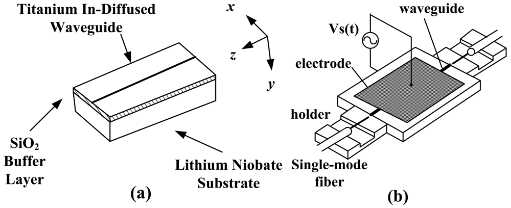
The integrated optical E-field sensor (IOES) has been extensively studied due to the rapid development of integrated optics. In general, a light waveguide is created on the LiNbO<sub>3</sub> substrate through Ti indiffusion or proton exchange, and the antenna/electrode is fabricated near the waveguide by photolithography [<xref ref-type="bibr" rid="b42-sensors-12-11406">42</xref>]. IOESs with various ranges of sensitivity and frequency bandwidth can be achieved by designing specific antennas and electrodes.</p>
<p>The purpose of this paper is to provide a comprehensive overview of the development and application of IOESs for intense E-field measurement and is organized as follows: In Section 2, three types of IOESs are classified and reviewed according to operating principle and sensor configuration. Recent progress and achievements are presented, and the characteristics of different types of IOESs are compared. On this basis, the improvement work of applying IOESs to intense E-field measurement is introduced. Section 3 illustrates the typical applications of intense E-field measurement using IOESs. The measurement of the DC field, power frequency AC field, μs-order transient field, and ns-order transient field are demonstrated for high-voltage engineering. The measurement of simulated NEMP is covered for HPEMs, and for high-energy physics, the measurement of the accelerating E-field of an ion accelerator is presented. Section 4 summarizes the conclusions of this paper and discusses the outlook for future IOES work.</p></sec></sec></sec>
<sec>
<label>2.</label>
<title>The Integrated Optical E-Field Sensor</title>
<p>
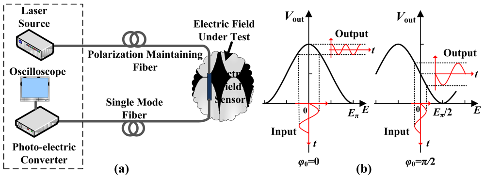
IOESs can be classified into three types according to differences in their waveguide structure and in their operating principle: the Mach-Zehnder Interferometer (MZI), the Coupler Interferometer (CI), and the Common Path Interferometer (CPI). The measurement system is illustrated schematically in <xref ref-type="fig" rid="f3-sensors-12-11406">Figure 3(a)</xref>. The linear polarized light generated by the laser source is transported to the sensor through a polarization-maintaining fiber. The optical signal is phase-modulated or polarization-state-modulated by the E-field as it passes through the waveguide. For the MZI or CI types, the phase modulation is transferred to intensity modulation at the output end of the waveguide. For the CPI type, the polarization-state modulation is changed to intensity modulation by the analyzer. The intensity signal is then delivered to the photo-electric converter by a single-mode fiber, where the optical signal is converted into an electrical signal. The sensor is situated in an intense electromagnetic environment, whereas the electronic devices are located in an electromagnetic shielding environment. The effective electrical isolation could be provided by the input/output fiber.</p>
<p>The ordinary Coupler Interferometer has a complicated transfer function [<xref ref-type="bibr" rid="b43-sensors-12-11406">43</xref>], while both the MZI and CPI have a simple sinusoidal type [<xref ref-type="bibr" rid="b43-sensors-12-11406">43</xref>,<xref ref-type="bibr" rid="b44-sensors-12-11406">44</xref>], expressed as:
<disp-formula id="FD1">
<label>(1)</label>
<mml:math id="mm1" display="block">
<mml:semantics id="sm1">
<mml:mrow>
<mml:msub>
<mml:mi>V</mml:mi>
<mml:mrow>
<mml:mtext>out</mml:mtext></mml:mrow></mml:msub>
<mml:mo>=</mml:mo>
<mml:mi>A</mml:mi>
<mml:mo>⋅</mml:mo>
<mml:mrow>
<mml:mo>[</mml:mo>
<mml:mrow>
<mml:mn>1</mml:mn>
<mml:mo>+</mml:mo>
<mml:mi>b</mml:mi>
<mml:mo>⋅</mml:mo>
<mml:mo>cos</mml:mo>
<mml:mo stretchy="false">(</mml:mo>
<mml:msub>
<mml:mi>φ</mml:mi>
<mml:mn>0</mml:mn></mml:msub>
<mml:mo>+</mml:mo>
<mml:mi>φ</mml:mi>
<mml:mo stretchy="false">(</mml:mo>
<mml:mi>E</mml:mi>
<mml:mo stretchy="false">)</mml:mo>
<mml:mo stretchy="false">)</mml:mo></mml:mrow>
<mml:mo>]</mml:mo></mml:mrow></mml:mrow></mml:semantics></mml:math></disp-formula>where <italic>A</italic> represents the optical power and photo-electric conversion coefficient; <italic>b</italic> represents the extinction ratio, usually ranging from 0.9 to 1; <italic>φ</italic><sub>0</sub> is the operating point, <italic>i.e.</italic>, the phase mismatch under a zero <italic>E</italic>-field; and <italic>φ</italic>(<italic>E</italic>) is the phase mismatch caused by the external E-field. The transfer function is illustrated in <xref ref-type="fig" rid="f3-sensors-12-11406">Figure 3(b)</xref>. Ideally, <italic>φ</italic><sub>0</sub> = π/2 (also known as the quadrature point), which results in an approximately linear input <italic>E</italic> and output <italic>V</italic><sub>out</sub> near this point. The output waveform is severely distorted, with <italic>φ</italic><sub>0</sub> deviating significantly from the quadrature point. <italic>φ</italic>(<italic>E</italic>) could be described as:
<disp-formula id="FD2">
<label>(2)</label>
<mml:math id="mm2" display="block">
<mml:semantics id="sm2">
<mml:mrow>
<mml:mi>φ</mml:mi>
<mml:mo stretchy="false">(</mml:mo>
<mml:mi>E</mml:mi>
<mml:mo stretchy="false">)</mml:mo>
<mml:mo>=</mml:mo>
<mml:mfrac>
<mml:mi>E</mml:mi>
<mml:mrow>
<mml:msub>
<mml:mi>E</mml:mi>
<mml:mrow>
<mml:mi mathvariant="normal">π</mml:mi></mml:mrow></mml:msub></mml:mrow></mml:mfrac>
<mml:mrow>
<mml:mi mathvariant="normal">π</mml:mi></mml:mrow></mml:mrow></mml:semantics></mml:math></disp-formula>where <italic>E</italic><sub>π</sub> is the E-field strength that results in a phase modulation equal to π (also shown in <xref ref-type="fig" rid="f3-sensors-12-11406">Figure 3</xref>). <italic>E</italic><sub>π</sub> is known as the half-wave E-field and determines the dynamic range of the sensor.</p>
<sec>
<label>2.1.</label>
<title>Mach-Zehnder Interferometer</title>
<sec>
<label>2.1.1.</label>
<title>Development of the MZI-Based E-Field Sensor</title>
<p>The typical structure of an IOES based on the MZI is shown in <xref ref-type="fig" rid="f4-sensors-12-11406">Figure 4</xref>. As the linear polarized light enters the waveguide, it is equally divided by the first Y-branch. The antenna and electrode amplify the external E-field. Next, the refractive index of the two waveguide arms are differently altered, resulting in a phase mismatch between the optical signals in the two arms. The two phase-modulated optical signals interfere with each other when they merge at the second Y branch. Consequently, the two optical signals become an intensity-modulated optical signal. The transfer function of the measurement system is expressed in <xref rid="FD1" ref-type="disp-formula">Equation (1)</xref>. To improve the sensitivity, the largest electro-optic coefficient <italic>γ</italic><sub>33</sub> is adopted, and the X-cut Y-propagating LiNbO<sub>3</sub> wafer is commonly used. <italic>φ</italic>(<italic>E</italic>) can be described as [<xref ref-type="bibr" rid="b45-sensors-12-11406">45</xref>]:
<disp-formula id="FD3">
<label>(3)</label>
<mml:math id="mm3" display="block">
<mml:semantics id="sm3">
<mml:mrow>
<mml:mi>φ</mml:mi>
<mml:mo stretchy="false">(</mml:mo>
<mml:mi>E</mml:mi>
<mml:mo stretchy="false">)</mml:mo>
<mml:mo>=</mml:mo>
<mml:mfrac>
<mml:mrow>
<mml:mn>2</mml:mn>
<mml:mrow>
<mml:mi mathvariant="normal">π</mml:mi></mml:mrow>
<mml:mi mathvariant="normal">Γ</mml:mi>
<mml:msup>
<mml:mrow>
<mml:msub>
<mml:mi>n</mml:mi>
<mml:mi>e</mml:mi></mml:msub></mml:mrow>
<mml:mn>3</mml:mn></mml:msup>
<mml:msub>
<mml:mi>r</mml:mi>
<mml:mrow>
<mml:mn>33</mml:mn></mml:mrow></mml:msub>
<mml:msub>
<mml:mi>L</mml:mi>
<mml:mrow>
<mml:mtext>el</mml:mtext></mml:mrow></mml:msub></mml:mrow>
<mml:mrow>
<mml:msub>
<mml:mi>λ</mml:mi>
<mml:mn>0</mml:mn></mml:msub></mml:mrow></mml:mfrac>
<mml:msub>
<mml:mi>E</mml:mi>
<mml:mrow>
<mml:mtext>in</mml:mtext></mml:mrow></mml:msub></mml:mrow></mml:semantics></mml:math></disp-formula>where Γ is the electro-optic overlap integral, representing the interaction of the E-field and the optical field; <italic>n</italic><sub>e</sub> is the extraordinary refractive index; <italic>L</italic><sub>el</sub> is the electrode length; <italic>λ</italic><sub>0</sub> is the vacuum wavelength; and <italic>E</italic><sub>in</sub> is the E-field imposed on the waveguide in the Z direction.</p>
<p>The LiNbO<sub>3</sub> material is a ferro-electric crystal with a pyro-electric property. A temperature change induces polarization charge that accumulates on the surfaces perpendicular to the principal axis [<xref ref-type="bibr" rid="b46-sensors-12-11406">46</xref>,<xref ref-type="bibr" rid="b47-sensors-12-11406">47</xref>]. Therefore, an additional E-field in the Z direction is generated by the pyro-electric effect. The amplitude of this field is estimated to be as high as ∼100 kV/m with a temperature variance of 1 °C [<xref ref-type="bibr" rid="b46-sensors-12-11406">46</xref>], resulting in an additional phase mismatch. <italic>φ</italic><sub>0</sub> can then be expressed as:
<disp-formula id="FD4">
<label>(4)</label>
<mml:math id="mm4" display="block">
<mml:semantics id="sm4">
<mml:mrow>
<mml:msub>
<mml:mi>φ</mml:mi>
<mml:mn>0</mml:mn></mml:msub>
<mml:mo>=</mml:mo>
<mml:msub>
<mml:mi>φ</mml:mi>
<mml:mtext>B</mml:mtext></mml:msub>
<mml:mo>+</mml:mo>
<mml:msub>
<mml:mi>φ</mml:mi>
<mml:mtext>T</mml:mtext></mml:msub></mml:mrow></mml:semantics></mml:math></disp-formula>where <italic>φ</italic><sub>T</sub> is the phase mismatch caused by temperature, mainly due to the pyro-electric effect, and <italic>φ</italic><sub>B</sub> is the optical bias, determined by the intrinsic optical path difference of the two arms.</p>
<p>
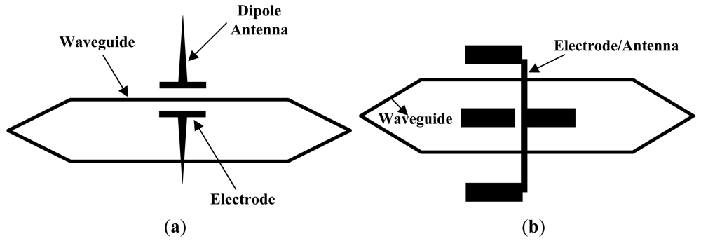
In the early stages of research in this field, an IOES based on MZI was used for RF tests in the EMC. The main objectives focused on the optimization of the antennas and electrodes to improve the sensitivity and frequency bandwidth. During the period from 1980 to 1995, the MZI-based IOES was first reported and comprehensively studied by Bulmer <italic>et al.</italic> at the NRL [<xref ref-type="bibr" rid="b46-sensors-12-11406">46</xref>–<xref ref-type="bibr" rid="b51-sensors-12-11406">51</xref>]. The fabricated sensor had a minimum detectable E-field of 1 V/m and a bandwidth of 300 MHz. As shown in <xref ref-type="fig" rid="f3-sensors-12-11406">Figure 3(b)</xref>, a value of <italic>φ</italic><sub>0</sub>∼π/2 is desirable, which requires <italic>φ</italic><sub>B</sub>∼π/2 and <italic>φ</italic><sub>T</sub>∼0 (see <xref rid="FD4" ref-type="disp-formula">Equation (4)</xref>). To ensure that <italic>φ</italic><sub>B</sub>∼π/2, the length difference of the two arms should be several micrometers. The errors in the photolithography and waveguide fabrication could not meet this accuracy requirement, leading to an uncontrollable value of <italic>φ</italic><sub>B</sub>. Laser ablation was proposed to improve the controllability of <italic>φ</italic><sub>B</sub> [<xref ref-type="bibr" rid="b50-sensors-12-11406">50</xref>,<xref ref-type="bibr" rid="b51-sensors-12-11406">51</xref>], as shown in <xref ref-type="fig" rid="f4-sensors-12-11406">Figure 4</xref>.</p>
<p>To maintain <italic>φ</italic><sub>T</sub>∼0, the two surfaces in the Z direction were short-circuited via a conducting paste, and a more favorable temperature stability was obtained [<xref ref-type="bibr" rid="b51-sensors-12-11406">51</xref>]. It should be noted that laser ablation requires complicated technology and that the short-circuit of the surfaces could also result in higher interference to the original field. From 1991 to 2002, Tajima <italic>et al.</italic> at the NTT Corp. developed high-sensitivity MZI-based IOESs, as shown in <xref ref-type="fig" rid="f5-sensors-12-11406">Figure 5(a)</xref> [<xref ref-type="bibr" rid="b52-sensors-12-11406">52</xref>–<xref ref-type="bibr" rid="b58-sensors-12-11406">58</xref>]. The resonance of the dipole antenna limits the high frequency characteristic of the sensor, and a resistive antenna was developed to expand the bandwidth [<xref ref-type="bibr" rid="b53-sensors-12-11406">53</xref>]. The measurement accuracy could be altered via the piezo-electric resonance phenomenon of the LiNbO<sub>3</sub> crystal; in other words, an E-field with a specific frequency stimulates the mechanical resonance of the crystal through the inverse piezo-electric effect, and the resulting strain alters the refractive index through the photo-elastic effect. The LiNbO<sub>3</sub> substrate was shaped as a trapezoid, dispersing the resonance energy and restraining the piezo-electric resonance phenomena, as shown in <xref ref-type="fig" rid="f5-sensors-12-11406">Figure 5(b)</xref> [<xref ref-type="bibr" rid="b56-sensors-12-11406">56</xref>]. To ensure that <italic>φ</italic><sub>B</sub>∼π/2, a method for adjusting <italic>φ</italic><sub>B</sub> via strain was proposed [<xref ref-type="bibr" rid="b57-sensors-12-11406">57</xref>]. A three-dimensional sensor was implemented by locating three one-dimensional sensors on the surfaces of a triangular prism; the fabricated sensor had a bandwidth greater than 10 GHz and a minimum detectable field of less than 22 mV/m [<xref ref-type="bibr" rid="b58-sensors-12-11406">58</xref>].</p>
<p>From 1992 to 1997, Petermann <italic>et al.</italic> at the Tech. Univ. Berlin developed IOESs with segmented modulator electrodes [<xref ref-type="bibr" rid="b59-sensors-12-11406">59</xref>–<xref ref-type="bibr" rid="b63-sensors-12-11406">63</xref>]. The antenna was located along the waveguide, reducing the equivalent input impedance and improving the match between the dipole antenna and the modulator, as shown in <xref ref-type="fig" rid="f6-sensors-12-11406">Figure 6(a)</xref>. The fabricated sensor had a sensitivity of 1 mV/m and a bandwidth of 3 GHz. A sealed sensor was also implemented to detect an E-field in liquid, as shown in <xref ref-type="fig" rid="f6-sensors-12-11406">Figure 6(b)</xref>.</p>
<p>
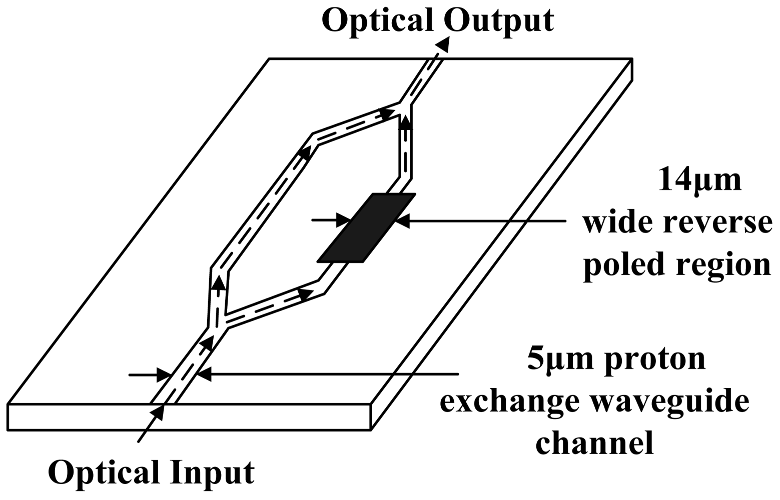
From 1994 to 1995, an MZI-based IOES with neither an antenna nor an electrode was developed separately by the Srico Corp. and the Univ. of British Columbia (UBC) [<xref ref-type="bibr" rid="b64-sensors-12-11406">64</xref>,<xref ref-type="bibr" rid="b65-sensors-12-11406">65</xref>]. The two arms of the MZI had different Ti-ion concentrations corresponding to a distinct Curie temperature. Under a certain temperature (e.g., 1,150 °C), domain inversion occurs in the area with a higher Ti-ion concentration, and the electro-optic coefficient is reversed. The two arms of the MZI have different electro-optic coefficients. The IOES developed by Srico Corp. had a minimum detectable field of 0.22 V/m and a bandwidth of 1 GHz, as shown in <xref ref-type="fig" rid="f7-sensors-12-11406">Figure 7</xref>.</p></sec>
<sec>
<label>2.1.2.</label>
<title>Improvement of Applying MZI Sensors to Intense E-Field Measurement</title>
<p>As stated above, past researchers focused on the RF field test, usually for amplitudes less than 1 V/m. The widely developed IOES performed well in high-frequency applications, but the low-frequency characteristics (DC to 10 kHz) of the sensor were rarely studied. Almost none of the MZI-based IOESs was designed for intense E-field measurement.</p>
<p>
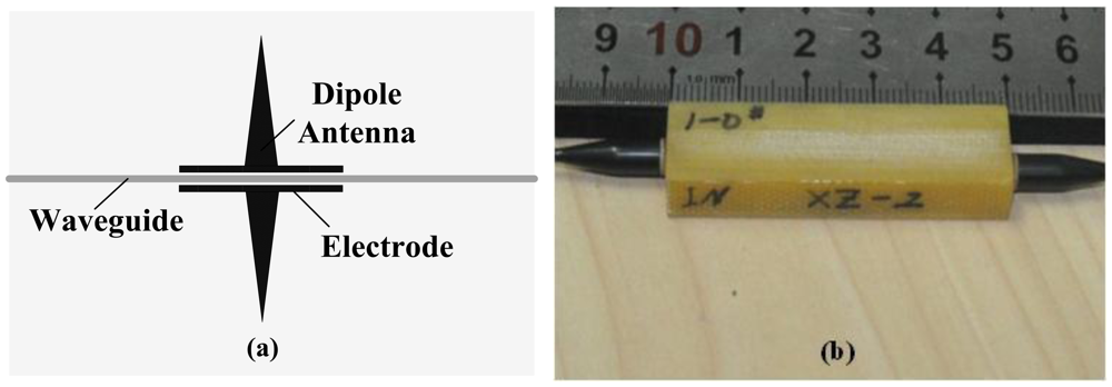
Based on existing knowledge and the requirements for measuring an intense E-field, the structures of the antenna and electrode were optimized, and IOESs suitable for intense E-field detection were developed by Tsinghua Univ. (THU) [<xref ref-type="bibr" rid="b45-sensors-12-11406">45</xref>]. The fabricated sensors have <italic>E</italic><sub>π</sub> ranges from ∼10 kV/m to ∼100 kV/m and a flat frequency response curve from the power frequency to greater than 100 MHz. For the design shown in <xref ref-type="fig" rid="f8-sensors-12-11406">Figure 8(a)</xref>, two electrodes with a distance of 40 μm were connected to the vertical dipole antennas with a length of 2 mm, and the <italic>E</italic><sub>π</sub> was approximately 600 kV/m. For the IOES illustrated in <xref ref-type="fig" rid="f8-sensors-12-11406">Figure 8(b)</xref>, dipole antennas were combined with the electrodes. The gap between the electrodes was enlarged to 100 μm, and the length of the antenna was shortened to 10 mm, leading to an <italic>E</italic><sub>π</sub> of approximately 70 kV/m.</p>
<p>
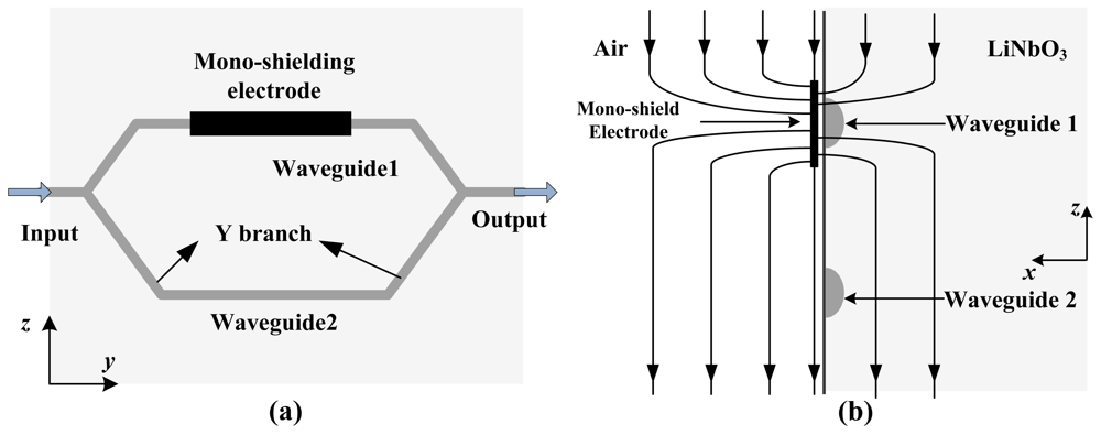
To expand the dynamic range, an IOES with a mono-shielding electrode was developed and is illustrated schematically in <xref ref-type="fig" rid="f9-sensors-12-11406">Figure 9</xref>. The E-field distribution around the waveguide is altered by the mono-shielding electrode, resulting in unbalanced modulation on the two arms of the MZI.</p>
<p>The mono-shielding gold electrode was fabricated by photolithography, with a thickness of 500 nm and a width of 100 μm. The fabricated sensors have <italic>E</italic><sub>π</sub> ranges from 2,000 kV/m to 8,000 kV/m; the <italic>E</italic><sub>π</sub> is altered by changing the length of the electrode (5 mm to 20 mm) and meets the requirement for air discharge field measurement.
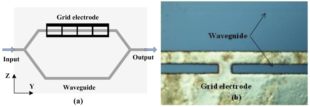
</p>
<p>A buffer layer (Si or SiO<sub>2</sub>) should be added between the waveguide and electrode to eliminate the influence of the metal on the waveguide. However, the buffer layer deteriorates the frequency response [<xref ref-type="bibr" rid="b66-sensors-12-11406">66</xref>] and the stability [<xref ref-type="bibr" rid="b67-sensors-12-11406">67</xref>]. The mono-shielding electrode was optimized as a grid type, shown in <xref ref-type="fig" rid="f10-sensors-12-11406">Figure 10</xref> [<xref ref-type="bibr" rid="b68-sensors-12-11406">68</xref>]. This improvement ameliorates the stability while maintaining the electrical characteristics of the sensor. The reduction of metal material may also generate less interference to the original field.</p>
<p>The MZI type is the most widely studied IOES; it has a simple geometrical structure with an <italic>E</italic><sub>π</sub> ranging from ∼1 V/m to ∼1 MV/m and is tuned using different types of antennas and electrodes. The key problems with this type of IOES are the controllability of <italic>φ</italic><sub>B</sub> and the stability of <italic>φ</italic><sub>0</sub>. The optical bias <italic>φ</italic><sub>B</sub> may severely deviate from the designed value due to errors in the photolithography and waveguide fabrication processes, and the operating point <italic>φ</italic><sub>0</sub> drifts drastically in response to temperature variations due to the pyro-electric effect. The drift rate is ∼1.25 °/°C for an ordinary MZI sensor and ∼5 °/°C for the domain inverse type [<xref ref-type="bibr" rid="b69-sensors-12-11406">69</xref>].</p></sec></sec>
<sec>
<label>2.2.</label>
<title>Coupler Interferometer</title>
<sec>
<label>2.2.1.</label>
<title>Development of the CI-Based E-Field Sensor</title>
<p>For MZI-based IOESs, the controllability of <italic>φ</italic><sub>B</sub> is improved by laser ablation [<xref ref-type="bibr" rid="b50-sensors-12-11406">50</xref>,<xref ref-type="bibr" rid="b51-sensors-12-11406">51</xref>] and strain adjustment [<xref ref-type="bibr" rid="b57-sensors-12-11406">57</xref>], although both processes add to fabrication complexity. Compared with the MZI, the Coupler Interferometer has a natural quadrature optical bias. The transmission and phase modulation of the optical signal in the waveguide is identical for the MZI and CI. The optical fields in the two arms of the CI couple with each other, thus changing the phase modulation to intensity modulation.</p>
<p>In 1986, Thaniyavam initially proposed the CI-based modulator. The experimental result is consistent with the theoretical analysis, and both show that the modulator has a quadrature optical bias [<xref ref-type="bibr" rid="b70-sensors-12-11406">70</xref>]. In 1988, Howerton <italic>et al.</italic> at the NRL created the CI-based IOES and compared the properties of IOESs based on the MZI and CI [<xref ref-type="bibr" rid="b71-sensors-12-11406">71</xref>]. Subsequently, a CI-based IOES with four ports, shown in <xref ref-type="fig" rid="f11-sensors-12-11406">Figure 11</xref>, was reported by Kanda <italic>et al.</italic> [<xref ref-type="bibr" rid="b43-sensors-12-11406">43</xref>].</p></sec>
<sec>
<label>2.2.2.</label>
<title>Improvement of Applying CI Sensors to Intense E-Field Measurement</title>
<p>
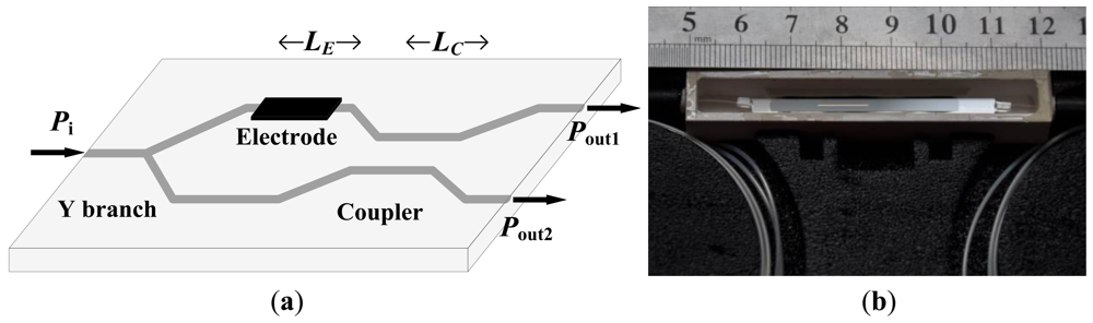
A CI-based IOES can improve the controllability of <italic>φ</italic><sub>B</sub>, but it has a complicated transfer function [<xref ref-type="bibr" rid="b70-sensors-12-11406">70</xref>]. A new CI-based IOES has been proposed that has a simple sinusoidal transfer function and a more favorable optical bias; this IOES has the advantages of both the MZI and conventional CI types [<xref ref-type="bibr" rid="b72-sensors-12-11406">72</xref>]. The structure of the novel sensor is shown in <xref ref-type="fig" rid="f12-sensors-12-11406">Figure 12(a)</xref>. The width of the waveguide was designated to be 6 μm to support a fundamental mode only. The distance of the coupler was selected as 7 μm, and the interaction length <italic>L</italic><sub>C</sub> was chosen as 2.8 mm. The fabricated sensor is shown in <xref ref-type="fig" rid="f12-sensors-12-11406">Figure 12(b)</xref> and has dimensions of 7 × 1 × 1 cm<sup>3</sup>.</p>
<p>The theoretical and experimental results of the transfer function are shown in <xref ref-type="fig" rid="f13-sensors-12-11406">Figure 13</xref>, both illustrating that the novel CI sensor has a sinusoid transfer function. Three sensors were fabricated, and their optical biases deviate from the ideal value by 3.3°, 7.9°, and 14.5°. This CI-based IOES has the ability to effectively improve the controllability of <italic>φ</italic><sub>B</sub>. The modified CI-based IOES has the advantages of the MZI type and improves the controllability of <italic>φ</italic><sub>B</sub>. However, the problem of the temperature stability of the operating point <italic>φ</italic><sub>0</sub> remains unsolved.</p></sec></sec>
<sec>
<label>2.3.</label>
<title>Common Path Interferometer</title>
<sec>
<label>2.3.1.</label>
<title>Development of the CPI-based E-Field Sensor</title>
<p>The potential advantage of the MZI lies in its high sensitivity; thus, the MZI-based IOES has been widely applied to the EMC test. Because the potential advantage of the CPI is high stability, it has drawn much attention in the area of voltage measurement and intense E-field detection. The structure of the CPI is illustrated in <xref ref-type="fig" rid="f14-sensors-12-11406">Figure 14</xref>.</p>
<p>
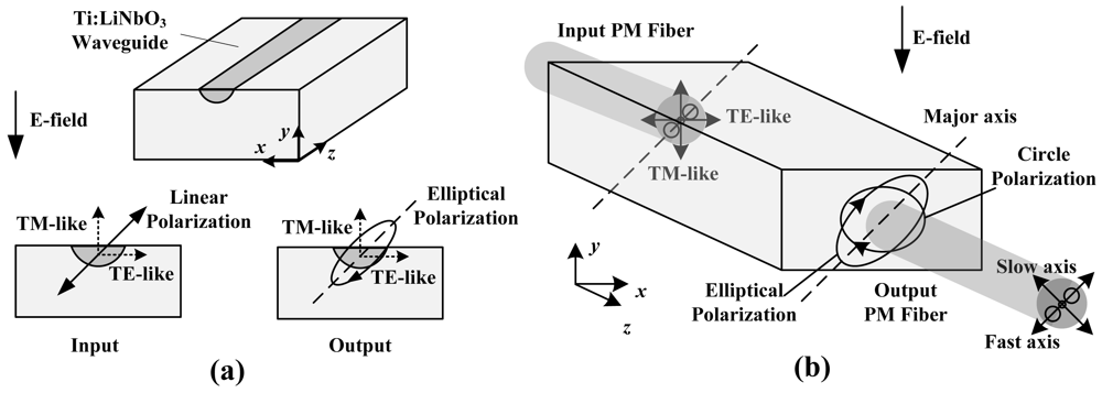
The Ti-indiffusion waveguide is constructed on a Z-propagating LiNbO<sub>3</sub> substrate. As linear polarized light enters the waveguide, it is divided into a TE mode and a TM mode. Imposing the E-field in the Y direction, <italic>n<sub>x</sub></italic> and <italic>n<sub>y</sub></italic> are modified as follows [<xref ref-type="bibr" rid="b73-sensors-12-11406">73</xref>]:
<disp-formula id="FD5">
<label>(5-1)</label>
<mml:math id="mm5" display="block">
<mml:semantics id="sm5">
<mml:mrow>
<mml:msub>
<mml:mi>n</mml:mi>
<mml:mrow>
<mml:mtext>TE</mml:mtext></mml:mrow></mml:msub>
<mml:mo>=</mml:mo>
<mml:msub>
<mml:mi>n</mml:mi>
<mml:mi>x</mml:mi></mml:msub>
<mml:mo>=</mml:mo>
<mml:msub>
<mml:mi>n</mml:mi>
<mml:mrow>
<mml:mrow>
<mml:mtext>o_TE</mml:mtext></mml:mrow></mml:mrow></mml:msub>
<mml:mo>+</mml:mo>
<mml:mfrac>
<mml:mn>1</mml:mn>
<mml:mn>2</mml:mn></mml:mfrac>
<mml:msubsup>
<mml:mi>n</mml:mi>
<mml:mtext>o</mml:mtext>
<mml:mn>3</mml:mn></mml:msubsup>
<mml:msub>
<mml:mi>γ</mml:mi>
<mml:mrow>
<mml:mn>22</mml:mn></mml:mrow></mml:msub>
<mml:msub>
<mml:mi>E</mml:mi>
<mml:mi>y</mml:mi></mml:msub></mml:mrow></mml:semantics></mml:math></disp-formula>
<disp-formula id="FD6">
<label>(5-2)</label>
<mml:math id="mm6" display="block">
<mml:semantics id="sm6">
<mml:mrow>
<mml:msub>
<mml:mi>n</mml:mi>
<mml:mrow>
<mml:mtext>TM</mml:mtext></mml:mrow></mml:msub>
<mml:mo>=</mml:mo>
<mml:msub>
<mml:mi>n</mml:mi>
<mml:mi>y</mml:mi></mml:msub>
<mml:mo>=</mml:mo>
<mml:msub>
<mml:mi>n</mml:mi>
<mml:mrow>
<mml:mrow>
<mml:mtext>o_TM</mml:mtext></mml:mrow></mml:mrow></mml:msub>
<mml:mo>−</mml:mo>
<mml:mfrac>
<mml:mn>1</mml:mn>
<mml:mn>2</mml:mn></mml:mfrac>
<mml:msubsup>
<mml:mi>n</mml:mi>
<mml:mtext>o</mml:mtext>
<mml:mn>3</mml:mn></mml:msubsup>
<mml:msub>
<mml:mi>γ</mml:mi>
<mml:mrow>
<mml:mn>22</mml:mn></mml:mrow></mml:msub>
<mml:msub>
<mml:mi>E</mml:mi>
<mml:mi>y</mml:mi></mml:msub></mml:mrow></mml:semantics></mml:math></disp-formula>where <italic>n</italic><sub>o</sub> is the ordinary refractive index. The refractive indices <italic>n</italic><sub>o_TE</sub> (X direction) and <italic>n</italic><sub>o_TM</sub> (Y direction) are slightly different due to the Ti indiffusion, <italic>γ</italic><sub>22</sub> is the electro-optic coefficient, and <italic>E<sub>y</sub></italic> is the E-field imposed on the waveguide in the Y direction.</p>
<p>When emitted from the waveguide, the TE mode and TM mode display a phase difference, and the light is transferred from linear polarization to elliptical polarization. The elliptically polarized light is analyzed by a polarization beam splitter (PBS) or by an analyzer. The transfer function of the measurement system is also presented in <xref rid="FD1" ref-type="disp-formula">Equation (1)</xref>. Similar to that of the MZI, the phase mismatch of the CPI could be described as <italic>φ</italic> = <italic>φ</italic>(<italic>E</italic>) + <italic>φ</italic><sub>B</sub> + <italic>φ</italic><sub>T</sub>:
<disp-formula id="FD7">
<label>(6-1)</label>
<mml:math id="mm7" display="block">
<mml:semantics id="sm7">
<mml:mrow>
<mml:mi>φ</mml:mi>
<mml:mo stretchy="false">(</mml:mo>
<mml:msub>
<mml:mi>E</mml:mi>
<mml:mi>y</mml:mi></mml:msub>
<mml:mo stretchy="false">)</mml:mo>
<mml:mo>≈</mml:mo>
<mml:mfrac>
<mml:mrow>
<mml:mn>2</mml:mn>
<mml:mrow>
<mml:mi mathvariant="normal">π</mml:mi></mml:mrow>
<mml:mi mathvariant="normal">Γ</mml:mi>
<mml:msup>
<mml:mrow>
<mml:msub>
<mml:mi>n</mml:mi>
<mml:mi>o</mml:mi></mml:msub></mml:mrow>
<mml:mn>3</mml:mn></mml:msup>
<mml:msub>
<mml:mi>r</mml:mi>
<mml:mrow>
<mml:mn>22</mml:mn></mml:mrow></mml:msub>
<mml:mi>L</mml:mi></mml:mrow>
<mml:mrow>
<mml:msub>
<mml:mi>λ</mml:mi>
<mml:mn>0</mml:mn></mml:msub></mml:mrow></mml:mfrac>
<mml:msub>
<mml:mi>E</mml:mi>
<mml:mi>y</mml:mi></mml:msub></mml:mrow></mml:semantics></mml:math></disp-formula>
<disp-formula id="FD8">
<label>(6-2)</label>
<mml:math id="mm8" display="block">
<mml:semantics id="sm8">
<mml:mrow>
<mml:msub>
<mml:mi>φ</mml:mi>
<mml:mtext>B</mml:mtext></mml:msub>
<mml:mo>=</mml:mo>
<mml:mfrac>
<mml:mrow>
<mml:mn>2</mml:mn>
<mml:mrow>
<mml:mi mathvariant="normal">π</mml:mi>
<mml:mo stretchy="false">(</mml:mo></mml:mrow>
<mml:msub>
<mml:mi>n</mml:mi>
<mml:mrow>
<mml:mrow>
<mml:mtext>o_TE</mml:mtext></mml:mrow></mml:mrow></mml:msub>
<mml:mo>−</mml:mo>
<mml:msub>
<mml:mi>n</mml:mi>
<mml:mrow>
<mml:mrow>
<mml:mtext>o_TM</mml:mtext></mml:mrow></mml:mrow></mml:msub>
<mml:mo stretchy="false">)</mml:mo>
<mml:mi>L</mml:mi></mml:mrow>
<mml:mrow>
<mml:msub>
<mml:mi>λ</mml:mi>
<mml:mn>0</mml:mn></mml:msub></mml:mrow></mml:mfrac>
<mml:mo>=</mml:mo>
<mml:mfrac>
<mml:mrow>
<mml:mn>2</mml:mn>
<mml:mrow>
<mml:mi mathvariant="normal">π</mml:mi></mml:mrow>
<mml:mi mathvariant="normal">Δ</mml:mi>
<mml:msub>
<mml:mi>n</mml:mi>
<mml:mtext>o</mml:mtext></mml:msub>
<mml:mi>L</mml:mi></mml:mrow>
<mml:mrow>
<mml:msub>
<mml:mi>λ</mml:mi>
<mml:mn>0</mml:mn></mml:msub></mml:mrow></mml:mfrac></mml:mrow></mml:semantics></mml:math></disp-formula>where <italic>L</italic> is the waveguide length. (<italic>n</italic><sub>o_TE</sub>-<italic>n</italic><sub>o_TM</sub>) is related to the waveguide width, such that <italic>φ</italic><sub>B</sub> could be controlled by changing the waveguide width.</p>
<p>Imposing the E-field in the Z direction, <italic>n<sub>x</sub></italic> and <italic>n<sub>y</sub></italic> are altered as follows [<xref ref-type="bibr" rid="b73-sensors-12-11406">73</xref>]:
<disp-formula id="FD9">
<label>(7-1)</label>
<mml:math id="mm9" display="block">
<mml:semantics id="sm9">
<mml:mrow>
<mml:msup>
<mml:mrow>
<mml:msub>
<mml:mi>n</mml:mi>
<mml:mrow>
<mml:mtext>TE</mml:mtext></mml:mrow></mml:msub></mml:mrow>
<mml:mo>′</mml:mo></mml:msup>
<mml:mo>=</mml:mo>
<mml:msub>
<mml:mi>n</mml:mi>
<mml:mrow>
<mml:mrow>
<mml:mtext>o_TE</mml:mtext></mml:mrow></mml:mrow></mml:msub>
<mml:mo>+</mml:mo>
<mml:mfrac>
<mml:mn>1</mml:mn>
<mml:mn>2</mml:mn></mml:mfrac>
<mml:msubsup>
<mml:mi>n</mml:mi>
<mml:mtext>o</mml:mtext>
<mml:mn>3</mml:mn></mml:msubsup>
<mml:msub>
<mml:mi>γ</mml:mi>
<mml:mrow>
<mml:mn>13</mml:mn></mml:mrow></mml:msub>
<mml:msub>
<mml:mi>E</mml:mi>
<mml:mi>z</mml:mi></mml:msub></mml:mrow></mml:semantics></mml:math></disp-formula>
<disp-formula id="FD10">
<label>(7-2)</label>
<mml:math id="mm10" display="block">
<mml:semantics id="sm10">
<mml:mrow>
<mml:msup>
<mml:mrow>
<mml:msub>
<mml:mi>n</mml:mi>
<mml:mrow>
<mml:mtext>TM</mml:mtext></mml:mrow></mml:msub></mml:mrow>
<mml:mo>′</mml:mo></mml:msup>
<mml:mo>=</mml:mo>
<mml:msub>
<mml:mi>n</mml:mi>
<mml:mrow>
<mml:mrow>
<mml:mtext>o_TM</mml:mtext></mml:mrow></mml:mrow></mml:msub>
<mml:mo>+</mml:mo>
<mml:mfrac>
<mml:mn>1</mml:mn>
<mml:mn>2</mml:mn></mml:mfrac>
<mml:msubsup>
<mml:mi>n</mml:mi>
<mml:mtext>o</mml:mtext>
<mml:mn>3</mml:mn></mml:msubsup>
<mml:msub>
<mml:mi>γ</mml:mi>
<mml:mrow>
<mml:mn>13</mml:mn></mml:mrow></mml:msub>
<mml:msub>
<mml:mi>E</mml:mi>
<mml:mi>z</mml:mi></mml:msub></mml:mrow></mml:semantics></mml:math></disp-formula></p>
<p>Next:
<disp-formula id="FD11">
<label>(8)</label>
<mml:math id="mm11" display="block">
<mml:semantics id="sm11">
<mml:mrow>
<mml:mi>φ</mml:mi>
<mml:mo stretchy="false">(</mml:mo>
<mml:msub>
<mml:mi>E</mml:mi>
<mml:mi>z</mml:mi></mml:msub>
<mml:mo stretchy="false">)</mml:mo>
<mml:mo>=</mml:mo>
<mml:mtext>O</mml:mtext></mml:mrow></mml:semantics></mml:math></disp-formula></p>
<p>The additional E-field caused by the pyro-electric effect is along the Z direction. Thus, <italic>φ</italic><sub>T</sub> approaches zero in theory, indicating that the CPI-based IOES will not be influenced by the pyro-electric effect and will have better temperature stability.</p>
<p>A comparison of the IOESs shown in <xref ref-type="fig" rid="f7-sensors-12-11406">Figure 7</xref> and <xref ref-type="fig" rid="f14-sensors-12-11406">Figure 14</xref> indicates that both are of the all-dielectric type. The <italic>E</italic><sub>π</sub> of the MZI type and the CPI type are presented as <xref rid="FD12" ref-type="disp-formula">Equation (9-1)</xref> and <xref rid="FD13" ref-type="disp-formula">Equation (9-2)</xref>, respectively. The E-field in this case is referred to as that imposed on the waveguide:
<disp-formula id="FD12">
<label>(9-1)</label>
<mml:math id="mm12" display="block">
<mml:semantics id="sm12">
<mml:mrow>
<mml:msup>
<mml:mrow>
<mml:msub>
<mml:mi>E</mml:mi>
<mml:mrow>
<mml:mrow>
<mml:mi mathvariant="normal">π</mml:mi>
<mml:mn>1</mml:mn></mml:mrow></mml:mrow></mml:msub></mml:mrow>
<mml:mo>′</mml:mo></mml:msup>
<mml:mo>=</mml:mo>
<mml:mfrac>
<mml:mrow>
<mml:msub>
<mml:mi>λ</mml:mi>
<mml:mn>0</mml:mn></mml:msub></mml:mrow>
<mml:mrow>
<mml:mn>2</mml:mn>
<mml:mi mathvariant="normal">Γ</mml:mi>
<mml:msup>
<mml:mrow>
<mml:msub>
<mml:mi>n</mml:mi>
<mml:mi>e</mml:mi></mml:msub></mml:mrow>
<mml:mn>3</mml:mn></mml:msup>
<mml:msub>
<mml:mi>r</mml:mi>
<mml:mrow>
<mml:mn>33</mml:mn></mml:mrow></mml:msub>
<mml:mi>L</mml:mi></mml:mrow></mml:mfrac></mml:mrow></mml:semantics></mml:math></disp-formula>
<disp-formula id="FD13">
<label>(9-2)</label>
<mml:math id="mm13" display="block">
<mml:semantics id="sm13">
<mml:mrow>
<mml:msup>
<mml:mrow>
<mml:msub>
<mml:mi>E</mml:mi>
<mml:mrow>
<mml:mrow>
<mml:mi mathvariant="normal">π</mml:mi>
<mml:mn>2</mml:mn></mml:mrow></mml:mrow></mml:msub></mml:mrow>
<mml:mo>′</mml:mo></mml:msup>
<mml:mo>=</mml:mo>
<mml:mfrac>
<mml:mrow>
<mml:msub>
<mml:mi>λ</mml:mi>
<mml:mn>0</mml:mn></mml:msub></mml:mrow>
<mml:mrow>
<mml:mn>2</mml:mn>
<mml:mi mathvariant="normal">Γ</mml:mi>
<mml:msup>
<mml:mrow>
<mml:msub>
<mml:mi>n</mml:mi>
<mml:mi>o</mml:mi></mml:msub></mml:mrow>
<mml:mn>3</mml:mn></mml:msup>
<mml:msub>
<mml:mi>r</mml:mi>
<mml:mrow>
<mml:mn>22</mml:mn></mml:mrow></mml:msub>
<mml:mi>L</mml:mi></mml:mrow></mml:mfrac></mml:mrow></mml:semantics></mml:math></disp-formula></p>
<p>The external E-field and that imposed on the waveguide have an approximate relation <italic>E</italic><sub>ex</sub> = <italic>εE</italic><sub>in</sub>, where <italic>ε</italic> is the dielectric constant. Assuming the domain-inversed waveguide length of the MZI is equal to the waveguide length of the CPI, the ratio is <italic>E</italic><sub>π1</sub>/<italic>E</italic><sub>π2</sub> ≈ (<italic>ε</italic><sub>33</sub>/<italic>ε</italic><sub>22</sub>) × (<italic>γ</italic><sub>22</sub>/<italic>γ</italic><sub>22</sub>) = 0.075 [<xref ref-type="bibr" rid="b74-sensors-12-11406">74</xref>]. The CPI-based IOES has an <italic>E</italic><sub>π</sub> that is 13 times larger than that of the domain inversed MZI sensor. With <italic>L</italic> = 10 mm and <italic>λ</italic><sub>0</sub> = 1,310 nm, the <italic>E</italic><sub>π</sub> of CPI is approximately 74 MV/m. Therefore, a notably large <italic>E</italic><sub>π</sub> is another feature of the CPI-based IOES.</p>
<p>In 1990, Jaeger <italic>et al.</italic> at UBC initially proposed the CPI-based IOES [<xref ref-type="bibr" rid="b75-sensors-12-11406">75</xref>]. The birefringence (<italic>n</italic><sub>o_TE</sub>-<italic>n</italic><sub>o_TM</sub>) caused by Ti indiffusion is related to the waveguide width. The waveguide with an optical bias close to π/2 could be obtained by designing waveguides with a series of widths on the same substrate [<xref ref-type="bibr" rid="b76-sensors-12-11406">76</xref>]. The relationship between the substrate dimension and the piezo-electric resonance frequency was studied, and it was concluded that <italic>f</italic><sub>r</sub> ≈ 6.8 /2<italic>w</italic> MHz (<italic>f</italic><sub>r</sub> is the lowest resonance frequency and <italic>w</italic> is the substrate width) [<xref ref-type="bibr" rid="b77-sensors-12-11406">77</xref>]. The schematic of the IOES is shown in <xref ref-type="fig" rid="f15-sensors-12-11406">Figure 15(a)</xref>, and the E-field sensor was eventually applied to the optical voltage transformer [<xref ref-type="bibr" rid="b78-sensors-12-11406">78</xref>].</p>
<p>In 1999, Ogawa <italic>et al.</italic> at the Tokyo Elec. Corp. studied and improved the temperature stability of this type of sensor [<xref ref-type="bibr" rid="b79-sensors-12-11406">79</xref>]. The sensor schematic is illustrated in <xref ref-type="fig" rid="f15-sensors-12-11406">Figure 15(b)</xref>. The coupling of the fiber and the waveguide was optimized, and the influence of the pyro-electric effect was further reduced by depositing an ITO film on the surfaces of the crystal perpendicular to the principal axis. The fluctuation of <italic>φ</italic><sub>0</sub> is as low as ±0.17 rad with the temperature varying from −30 °C to 90 °C.</p></sec>
<sec>
<label>2.3.2.</label>
<title>Improvement of Applying CPI Sensors to Intense E-Field Measurement</title>
<p>The main objective of UBC and the Tokyo Elec. Corp. was to apply the CPI-based IOES to voltage measurement. Since 1994, Takahashi <italic>et al.</italic> have worked on development of this type of sensor and applied it to discharge field measurement [<xref ref-type="bibr" rid="b80-sensors-12-11406">80</xref>–<xref ref-type="bibr" rid="b82-sensors-12-11406">82</xref>]. To improve the spatial resolution, a CPI sensor with a small dimension (1 × 0.39 × 0.6 mm<sup>3</sup>) was produced, as shown in <xref ref-type="fig" rid="f16-sensors-12-11406">Figure 16</xref>.</p>
<p>The half-wave E-field of the sensor developed by Takahashi is greater than 100 MV/m. According to the analysis in Section 1, the magnitude of an intense E-field measurement primarily ranges from ∼1 kV/m to ∼1 MV/m. The sensitivity of the CPI-based IOES is so low that it was not able to meet most of the requirements of the applications in measurement of intense E-fields.</p>
<p>To improve the sensitivity, THU designed antennas and electrodes around the waveguide, as shown in <xref ref-type="fig" rid="f17-sensors-12-11406">Figure 17(a)</xref>. The Ti-indiffusion waveguide has a length of 2 mm and a width ranging from 10 μm to 12 μm; the antenna has a length of 2 mm, and the electrode has variable dimensions for different <italic>E</italic><sub>π</sub>. The IOES after encapsulation is shown in <xref ref-type="fig" rid="f17-sensors-12-11406">Figure 17(b)</xref>. This type of sensor could be shorter than the MZI or CI types. Because the waveguide with a favorable optical bias in the CPI could have a length on the order of millimeters, the Y branch of the MZI or CI limits the reduction of the waveguide length.</p>
<p>The fabricated sensors have an <italic>E</italic><sub>π</sub> of approximately 2,500 kV/m, and the optical biases deviate from the ideal values within 8°, as shown in <xref ref-type="table" rid="t1-sensors-12-11406">Table 1</xref>. The operating point <italic>φ</italic><sub>0</sub> varies slowly with temperature, and the drift rate is approximately 0.015 °/°C/mm (the waveguide length is 20 mm), as shown in <xref ref-type="fig" rid="f18-sensors-12-11406">Figure 18</xref>. This value is similar to the 0.014 °/°C/mm value reported by UBC [<xref ref-type="bibr" rid="b68-sensors-12-11406">68</xref>], and both demonstrate that the CPI-based IOES has much better temperature stability.</p>
<p>The CPI-based IOES has overcome the key problems of the MZI or CI types: controllability of the optical bias and temperature stability of the operating point. By designing dipole antennas and electrodes, the dynamic range of the optimized sensor is able to meet the requirement of intense E-field measurement.</p></sec></sec>
<sec>
<label>2.4.</label>
<title>Characteristic Comparison of IOES</title>
<p>Comparison of the three types of IOESs yields the following observations:
<list list-type="order">
<list-item>
<p>The MZI type is most widely studied. It has a simple geometrical structure, and <italic>E</italic><sub>π</sub> ranges from ∼1 V/m to ∼1 MV/m can be realized by varying the design of the antennas and electrodes. The key problem is that the optical bias <italic>φ</italic><sub>B</sub> is difficult to control and that the operating point <italic>φ</italic><sub>0</sub> is severely affected by temperature.</p></list-item>
<list-item>
<p>The CI type has a natural quadrature <italic>φ</italic><sub>B</sub>. The improved sensor has both a better <italic>φ</italic><sub>B</sub> and a simple sinusoidal transfer function. Similar to the MZI, the temperature stability of <italic>φ</italic><sub>0</sub> remains a challenge.</p></list-item>
<list-item>
<p>The CPI type could effectively solve the problems that exist in the other two types. The advantages of the CPI type include the following: a <italic>φ</italic><sub>B</sub> close to the quadrature point can be obtained by selecting the waveguide width. The pyro-electric effect has no influence on <italic>φ</italic><sub>0</sub> in theory, and the sensor has much better temperature stability in practice. However, the disadvantages are that the sensor adopts the smaller electro-optic coefficient <italic>γ</italic><sub>22</sub> and the larger dielectric constant <italic>ε</italic><sub>22</sub>, resulting in a lower sensitivity. An additional polarizer and PBS are needed, thus increasing the complexity of the optical system. The characteristics of the three types of IOESs are summarized in <xref ref-type="table" rid="t2-sensors-12-11406">Table 2</xref>.</p></list-item></list></p></sec></sec>
<sec>
<label>3.</label>
<title>Typical Applications of Intense E-Field Measurement</title>
<sec>
<label>3.1.</label>
<title>E-Field Measurement in High-Voltage Engineering</title>
<sec>
<label>3.1.1.</label>
<title>DC E-Field Measurement</title>
<p>Cecelja <italic>et al.</italic> has studied DC field measurement based on bulk optic sensors [<xref ref-type="bibr" rid="b29-sensors-12-11406">29</xref>–<xref ref-type="bibr" rid="b31-sensors-12-11406">31</xref>]. The discrete optical components can only be located on the optical bench, which is not realistic for practical measurements. A MZI-based IOES with a mono-shielding electrode was primarily used to measure the DC field without space charge [<xref ref-type="bibr" rid="b83-sensors-12-11406">83</xref>].</p>
<p>
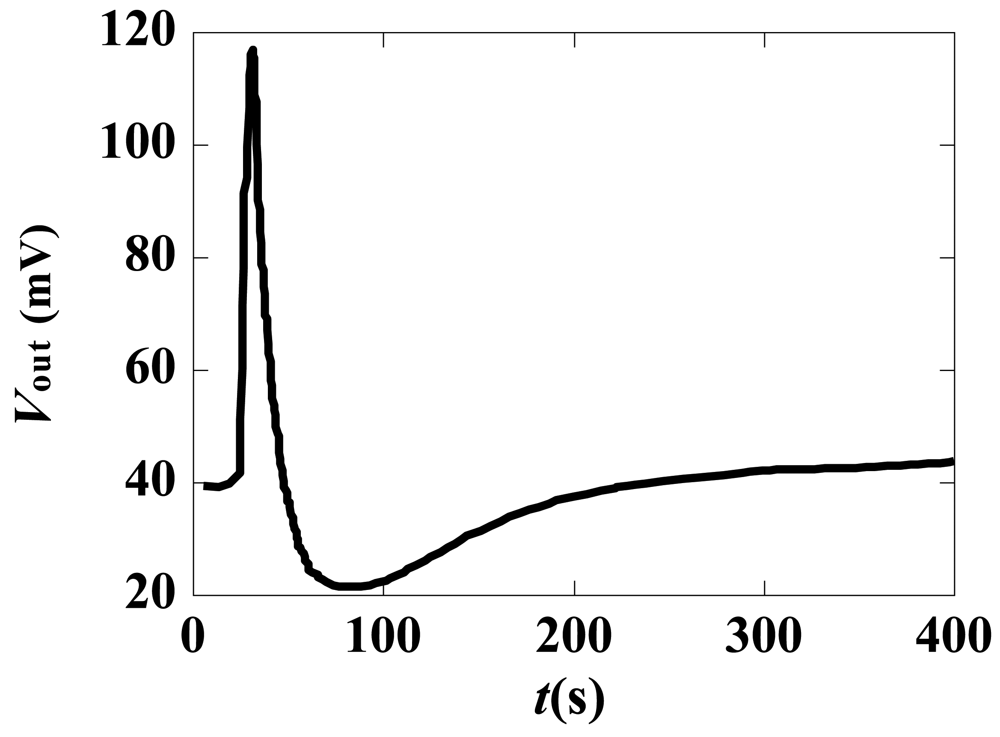
The step response of the sensor is shown in <xref ref-type="fig" rid="f19-sensors-12-11406">Figure 19</xref>. The sensor has a rapidly decaying response due to the dielectric property of the LiNbO<sub>3</sub> crystal [<xref ref-type="bibr" rid="b38-sensors-12-11406">38</xref>]; therefore, the sensor cannot directly measure the DC field.</p>
<p>An approximately rectangular pulse was applied to the sensor, and the frequency response of the measurement system was obtained via Fast Fourier Transform (FFT), shown in <xref ref-type="fig" rid="f20-sensors-12-11406">Figure 20</xref>. A vector fitting with three poles and three zeros was performed, and the fitting results are also displayed in <xref ref-type="fig" rid="f20-sensors-12-11406">Figure 20</xref>.</p>
<p>
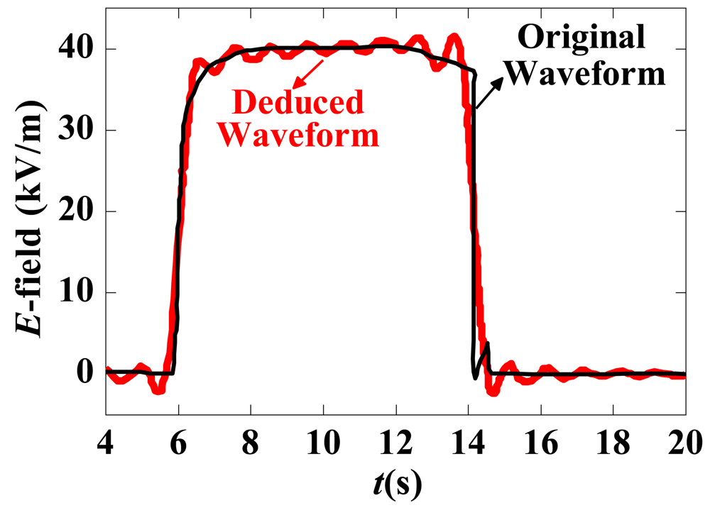
Obtaining the time-domain response under a rectangular pulse E-field together with the frequency response curve of the measurement system, the time-domain input waveform can be restored. The deduced excitation waveform is shown in <xref ref-type="fig" rid="f21-sensors-12-11406">Figure 21</xref>, as is the original excitation waveform; the two waveforms are almost identical.</p></sec></sec>
<sec>
<label>3.1.2.</label>
<title>AC Power Frequency E-Field Measurement</title>
<p>
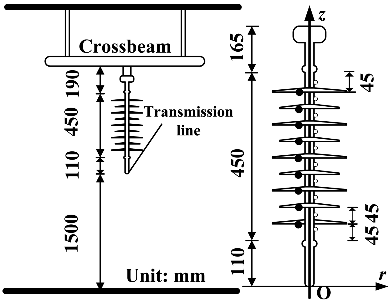
Measurement of the power frequency E-field distribution along composite insulators is important for the optimization of the insulator structure [<xref ref-type="bibr" rid="b84-sensors-12-11406">84</xref>]. The experimental configuration is shown in <xref ref-type="fig" rid="f22-sensors-12-11406">Figure 22</xref>, which simulates the arrangement of suspension insulators on a tower. The E-field sensor was fixed by an insulated bracket to ensure the proper position of the sensor. The output voltage of the power frequency transformer was fixed at 35 kV during the experiment.</p>
<p>The axial component (direction <italic>z</italic> in <xref ref-type="fig" rid="f22-sensors-12-11406">Figure 22</xref>) of the E-field was measured first. The measured positions were selected at the middle of each of two sheds and were numbered from 1 to 10 in sequence from highest to lowest potential, illustrated in <xref ref-type="fig" rid="f22-sensors-12-11406">Figure 22</xref> as hollow circles. The radial E-field component (direction <italic>r</italic> in <xref ref-type="fig" rid="f22-sensors-12-11406">Figure 22</xref>) was measured as well. The measurement positions were selected just below each shed and were numbered from 1 to 9 in sequence from highest to lowest potential, shown in <xref ref-type="fig" rid="f22-sensors-12-11406">Figure 22</xref> as solid circles. The surface of the sensor contacted the surface of the shed as closely as possible.</p>
<p>The measurement and calculation results of the RMS value of the E-field were obtained and are shown in <xref ref-type="fig" rid="f23-sensors-12-11406">Figure 23</xref> (with <italic>r</italic> = 30 mm). The measured and calculated curves are similar. The distribution of the axial E-field is U-shaped, and the distribution of the radial E-field is monotonously decreased.</p>
<sec>
<label>3.1.3.</label>
<title>Air Gap Discharge E-Field Measurement [<xref ref-type="bibr" rid="b85-sensors-12-11406">85</xref>,<xref ref-type="bibr" rid="b86-sensors-12-11406">86</xref>]</title>
<p>
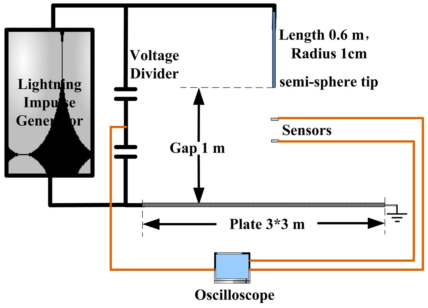
The IOES is able to effectively respond to a standard lightning wave (1.2/50 μs) and an EMP with an ns-order rise time [<xref ref-type="bibr" rid="b85-sensors-12-11406">85</xref>]. The performance of the adopted sensor is adequate for measuring the E-field in air gap discharges. After calibrating the sensor, a rod-plane discharge experiment under positive lightning impulse was designed and is shown in <xref ref-type="fig" rid="f24-sensors-12-11406">Figure 24</xref>. A rod with a semi-spherical tip with a 1 cm radius was hung at a height of 1 m above a well-grounded plane. The E-field sensors were placed in the gap at distances ranging from 30 cm to 70 cm above the plane.
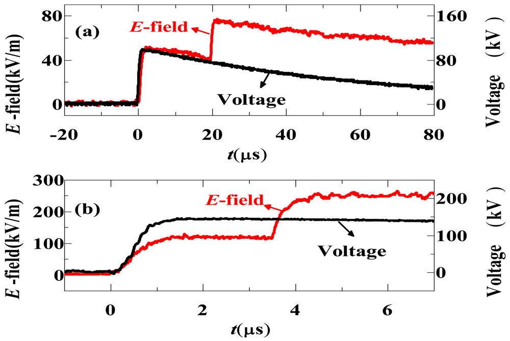
</p>
<p>Typical results are shown in <xref ref-type="fig" rid="f25-sensors-12-11406">Figure 25</xref>. When the applied voltage is low, the space E-field followed the applied voltage with less than 5% error. When the voltage reached a specific level (e.g., above 200 kV under the experimental conditions), the space E-field was distorted. The E-field strength suddenly increased ΔE, and an E-field step with a rapid rise time was observed. The E-field step was shown to be caused by the space net charge. From the E-step rise time and the corona area range, the average electron drift speed under the experiment situation was estimated to be approximately 0.2 × 10<sup>6</sup> to 0.6 × 10<sup>6</sup> m/s.</p></sec>
<sec>
<label>3.1.4.</label>
<title>VFTO E-Field Measurement [<xref ref-type="bibr" rid="b87-sensors-12-11406">87</xref>]</title>
<p>Very fast transient overvoltages (VFTOs) are generated by system faults or switching operations in the GIS. The travelling wave has a fundamental frequency of ∼10 MHz due to the compacted structure of the GIS. High-frequency components of ∼100 MHz superposed on the fundamental frequency component are generated due to the refraction and reflection of the travelling wave between different devices.</p>
<p>
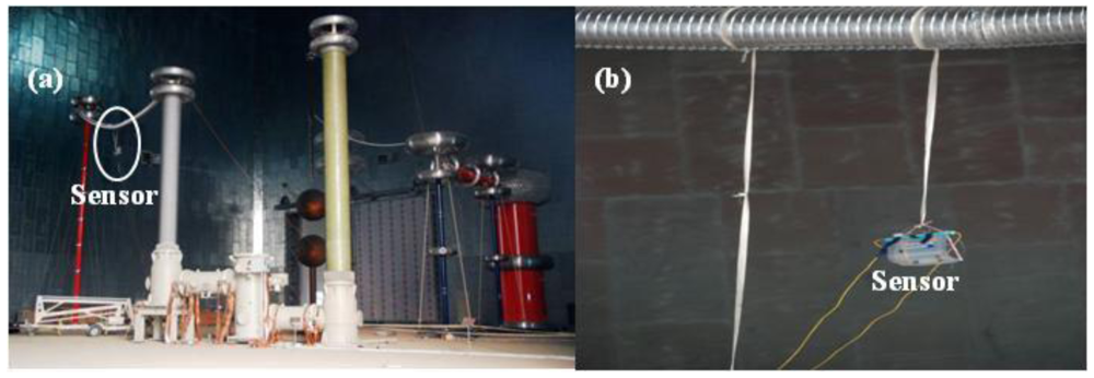
The measuring system developed by THU was applied to a 1,000-kV GIS test setup. <xref ref-type="fig" rid="f26-sensors-12-11406">Figure 26(a)</xref> shows the global view of the equipment: the 1,000-kV experimental transformer is connected to the gas insulated switchgear by the protection resistor, and the output of the switchgear is connected to a capacitive load. The sensor was placed 1 m beneath the center of the long conductor that connects the load and the switchgear, as shown in <xref ref-type="fig" rid="f26-sensors-12-11406">Figure 26(b)</xref>.</p>
<p>
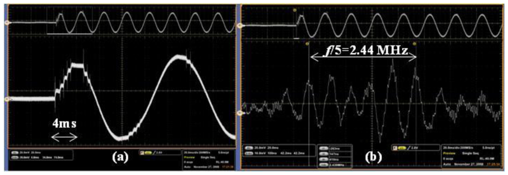
The transient E-field was measured during a close-operation of the disconnector with an RMS AC voltage of 680 kV. As shown in <xref ref-type="fig" rid="f27-sensors-12-11406">Figure 27(a)</xref>, the process of the close-operation lasts for approximately one power frequency cycle. With the expansion of <xref ref-type="fig" rid="f27-sensors-12-11406">Figure 27(a)</xref>, it was observed that the fundamental frequency is approximately 12 MHz, shown in <xref ref-type="fig" rid="f27-sensors-12-11406">Figure 27(b)</xref>. The overvoltage is approximately 1.78 p.u. considering the most serious condition in which the high frequency components are superposed on the peak of the power frequency component.</p></sec></sec>
<sec>
<label>3.2.</label>
<title>E-Field Measurement in HPEM</title>
<p>
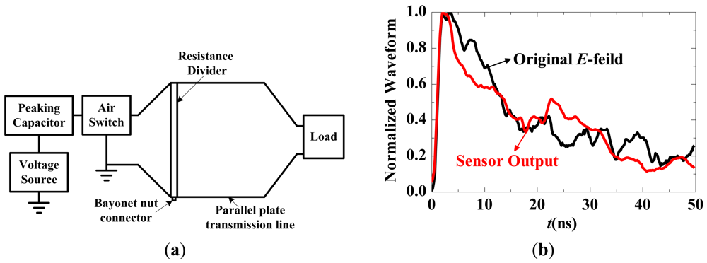
The nuclear electromagnetic pulse (NEMP) generally has a double exponential pulse shape with a rise time of a few ns, a maximum E-field strength of 50 kV/m, and a full-width half-max time of 200–400 ns [<xref ref-type="bibr" rid="b5-sensors-12-11406">5</xref>]. The simulated NEMP can be generated by an NEMP simulator [<xref ref-type="bibr" rid="b88-sensors-12-11406">88</xref>] such as a high voltage source, a gas discharge switch and a transverse electromagnetic strip transmission line, as shown in <xref ref-type="fig" rid="f28-sensors-12-11406">Figure 28(a)</xref>. The voltage source is connected to the input end of the gas discharge switch through the peaking capacitor. The terminal of the transmission line is a matched load comprising metal film resistors. The voltage U between the transmission lines can be measured by the resistor divider, and the E-field at the central point can be calculated using U/d (where d is the separation of the transmission line). The sensor is located at the central point, and the electronic devices are housed in a screened room.</p>
<p>The simulated NEMP has a rise time of approximately 1.2 ns. The normalized waveforms of the original E-field and the sensor output are shown in <xref ref-type="fig" rid="f28-sensors-12-11406">Figure 28(b)</xref>, indicating that the IOES has a response time less than 1.2 ns.</p></sec>
<sec>
<label>3.3.</label>
<title>E-Field Measurement in High-Energy Physics</title>
<p>
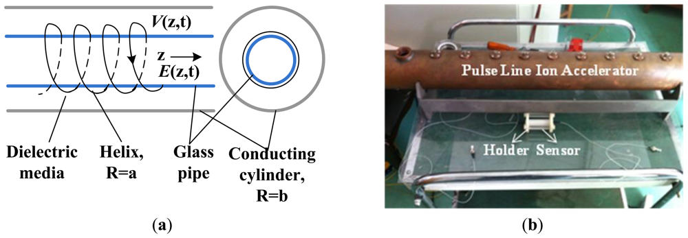
A pulse line ion accelerator (PLIA) is a new type of heavy ion accelerator that was developed to meet the need for studying High Energy Density Physics and Warm Dense Matter. Due to the limited space inside the PLIA (cm order), the large E-field strength (kV/m order), and the high frequency (MHz order), measuring the accelerating E-field of the PLIA is difficult [<xref ref-type="bibr" rid="b7-sensors-12-11406">7</xref>]. The structure of the PLIA is schematically illustrated in <xref ref-type="fig" rid="f29-sensors-12-11406">Figure 29(a)</xref>, and a picture of a PLIA prototype is shown in <xref ref-type="fig" rid="f29-sensors-12-11406">Figure 29(b)</xref>. The interior glass pipe has a length of 90 cm and a diameter of 52 mm. The cross-sectional dimension of the IOES is 10 mm, which is suitable for measurement of the PLIA field.</p>
<p>The E-field waveforms on the axis of the PLIA are shown in <xref ref-type="fig" rid="f30-sensors-12-11406">Figure 30(a)</xref>. The three measurement points are located at 25 cm, 45 cm and 65 cm away from the front end of the glass pipe. The waveforms appear quite similar in different locations, indicating that the propagation of the electromagnetic field is nearly lossless. With an input voltage of 1 kV, the peak value of the E-field on the axis is approximately 2.9 kV/m. A simulation model of the PLIA was built using the Finite Integration Technique, and the simulated waveform is in agreement with the measured one, as shown in <xref ref-type="fig" rid="f30-sensors-12-11406">Figure 30(b)</xref>.</p></sec></sec>
<sec sec-type="conclusions">
<label>5.</label>
<title>Conclusions/Outlook</title>
<p>Since the 1980s, the rapid growth of integrated optics technology has led to an increase in worldwide research on integrated optical sensors. Time domain electric and magnetic field measurements are key research topics for scientific work in areas such as high-voltage engineering, high-power electromagnetic pulses, and high-energy physics. Until recently, in these research areas, only integrated optical E-field sensors (IOESs) were able to satisfy most of the application requirements, which include a small size (mm), broadband response (DC ∼ GHz), high signal amplitude (kV/m∼MV/m), and appropriate insulation (MV).</p>
<p>In the search for clear advantages, researchers from the USA, Canada, Japan, Germany and China have focused on the IOES advancements that have been achieved over the past 30 years. These researchers have developed a wide variety of IOES designs, and some have been implemented and applied in practice. As this review details, the Mach-Zehnder interferometer (MZI), coupler interferometer (CI) and common path interferometer (CPI) are the fundamental structures that have been most widely adopted in those designs.</p>
<p>The improvements in applications of IOESs to intense E-field measurement are presented in this work. The theoretical concerns and specific characteristics of these IOESs are illustrated in terms of their structures and key parameters. Finally, selected applications of intense E-field measurement in various research areas are introduced for measuring the time-domain waveform in the nanosecond to microsecond, millisecond, and DC ranges. These applications indicate that IOESs are useful in these applications and will be put into broad use in transient measurement research in areas such as natural lightning physics, gas discharge physics, and HPEMs, among others.</p>
<p>In spite of the prominent advantages and enormous potential of IOESs, challenges still remain for improving IOES performance and expanding their scope of application. First, the operating stability (especially the stability with the temperature variance) should be improved in the future. The mechanism of temperature stability should be studied in-depth, and new materials, innovative structures and design measures should be explored. Second, our experiments and those of others have demonstrated that humidity affects the performance of the sensor; for example, the phase shift between the input and output signals changes with the humidity. Humidity may have additional impacts on the sensor that we have not observed; these impacts should be investigated in detail. Third, the encapsulation of the small sensor should be improved. New packaging materials and techniques should be applied, and the size could be further decreased not only for more accurate measurement but also for reducing the distortion of the original E-field. Fourth, additional work must be conducted for the time-domain and frequency-domain calibration of the intense E-field sensor because it is very difficult to generate a standard field that is sufficiently strong. Finally, questions that are clearly important for on-site applications remain; for example, it remains to be determined how the distortion caused by the sensor in different circumstances should be evaluated and how the accurate original E-field should be obtained. All of the above challenges will motivate continued research in this field.</p></sec></body>
<back>
<ack>
<p>This work was supported by the Fund of the National Priority Basic Research of China (2011CB209403) and the National Natural Science Foundation of China under Grant 51107063.</p></ack>
<ref-list>
<title>References</title>
<ref id="b1-sensors-12-11406"><label>1.</label><citation citation-type="journal"><person-group person-group-type="author"><name><surname>Bahrman</surname><given-names>M.P.</given-names></name><name><surname>Johnson</surname><given-names>B.K.</given-names></name></person-group><article-title>The ABCs of HVDC transmission technologies</article-title><source>IEEE Power Energy Mag.</source><year>2007</year><volume>5</volume><fpage>32</fpage><lpage>44</lpage></citation></ref>
<ref id="b2-sensors-12-11406"><label>2.</label><citation citation-type="book"><person-group person-group-type="author"><name><surname>Comber</surname><given-names>M.</given-names></name><name><surname>Nigbor</surname><given-names>R.</given-names></name><name><surname>Zaffanella</surname><given-names>L.</given-names></name></person-group><source>Transmission Line Reference Book-345 kV and Above</source><publisher-name>EPRI</publisher-name><publisher-loc>Palo Alto, CA, USA</publisher-loc><year>1987</year><comment>Chapter 6</comment></citation></ref>
<ref id="b3-sensors-12-11406"><label>3.</label><citation citation-type="journal"><person-group person-group-type="author"><name><surname>Hidaka</surname><given-names>K.</given-names></name></person-group><article-title>Progress in Japan of space charge field measurement in gaseous dielectric using a pockels sensor</article-title><source>IEEE Electr. Insul. Mag.</source><year>1996</year><volume>12</volume><fpage>17</fpage><lpage>28</lpage></citation></ref>
<ref id="b4-sensors-12-11406"><label>4.</label><citation citation-type="journal"><person-group person-group-type="author"><name><surname>Meppelink</surname><given-names>J.</given-names></name><name><surname>Diederich</surname><given-names>K.J.</given-names></name><name><surname>Feser</surname><given-names>K.</given-names></name><name><surname>Pfaff</surname><given-names>W.R.</given-names></name></person-group><article-title>Very fast transients in GIS</article-title><source>IEEE Trans. Power Deliv.</source><year>1989</year><volume>4</volume><fpage>223</fpage><lpage>233</lpage><pub-id pub-id-type="doi">10.1109/61.19208</pub-id></citation></ref>
<ref id="b5-sensors-12-11406"><label>5.</label><citation citation-type="journal"><person-group person-group-type="author"><name><surname>Daniel</surname><given-names>N.</given-names></name><name><surname>Camp</surname><given-names>M.</given-names></name><name><surname>Sabath</surname><given-names>F.</given-names></name><name><surname>Haseborg</surname><given-names>J.L.</given-names></name><name><surname>Garbe</surname><given-names>H.</given-names></name></person-group><article-title>Susceptibility of some electronic equipment to HPEM threats</article-title><source>IEEE Trans. Electr. Comput.</source><year>2004</year><volume>46</volume><fpage>380</fpage><lpage>389</lpage><pub-id pub-id-type="doi">10.1109/TEMC.2004.831842</pub-id></citation></ref>
<ref id="b6-sensors-12-11406"><label>6.</label><citation citation-type="journal"><person-group person-group-type="author"><name><surname>Radasky</surname><given-names>W.A.</given-names></name><name><surname>Baum</surname><given-names>C.E.</given-names></name><name><surname>Wik</surname><given-names>M.W.</given-names></name></person-group><article-title>Introduction to the special issue on High-Power Electromagnetics (HPEM) and Intentional Electromagnetic Interference (IEMI)</article-title><source>IEEE Trans. Electr. Comput.</source><year>2004</year><volume>46</volume><fpage>314</fpage><lpage>321</lpage><pub-id pub-id-type="doi">10.1109/TEMC.2004.831899</pub-id></citation></ref>
<ref id="b7-sensors-12-11406"><label>7.</label><citation citation-type="journal"><person-group person-group-type="author"><name><surname>Briggs</surname><given-names>R.J.</given-names></name></person-group><article-title>Pulse line ion accelerator concept</article-title><source>Phys. Rev. ST Accel. Beams</source><year>2006</year><volume>9</volume><fpage>060401:1</fpage><lpage>060401:16</lpage></citation></ref>
<ref id="b8-sensors-12-11406"><label>8.</label><citation citation-type="confproc"><person-group person-group-type="author"><name><surname>Caporaso</surname><given-names>G.J.</given-names></name><name><surname>Sampayan</surname><given-names>S.</given-names></name><name><surname>Chen</surname><given-names>Y.-J.</given-names></name><name><surname>Blackfield</surname><given-names>D.</given-names></name><name><surname>Harris</surname><given-names>J.</given-names></name><name><surname>Hawkins</surname><given-names>S.</given-names></name><name><surname>Holmes</surname><given-names>C.</given-names></name><name><surname>Krogh</surname><given-names>M.</given-names></name><name><surname>Nelson</surname><given-names>S.</given-names></name><name><surname>Nunnally</surname><given-names>W.</given-names></name><etal/></person-group><article-title>High Gradient Induction Accelerator</article-title><conf-name>Proceedings of the IEEE Particle Accelerator Conference</conf-name><conf-loc>Albuquerque, NM, USA</conf-loc><conf-date>25–29 June 2007</conf-date><fpage>857</fpage><lpage>861</lpage></citation></ref>
<ref id="b9-sensors-12-11406"><label>9.</label><citation citation-type="journal"><person-group person-group-type="author"><name><surname>Shen</surname><given-names>X.-K.</given-names></name><name><surname>Cao</surname><given-names>S.-C.</given-names></name><name><surname>Zhang</surname><given-names>Z.-M.</given-names></name><name><surname>Zhao</surname><given-names>H.-W.</given-names></name><name><surname>Zhao</surname><given-names>Q.-T.</given-names></name><name><surname>Liu</surname><given-names>M.</given-names></name><name><surname>Jing</surname><given-names>Y.</given-names></name><name><surname>Li</surname><given-names>Z.-P.</given-names></name><name><surname>Wan</surname><given-names>M.</given-names></name><name><surname>Wang</surname><given-names>B.</given-names></name><etal/></person-group><article-title>The test pulse line ion accelerator in Lanzhou</article-title><source>CPC(HEP &amp; NP)</source><year>2012</year><volume>36</volume><fpage>241</fpage><lpage>246</lpage></citation></ref>
<ref id="b10-sensors-12-11406"><label>10.</label><citation citation-type="journal"><person-group person-group-type="author"><name><surname>Masamitsu</surname><given-names>T.</given-names></name><name><surname>Nobuo</surname><given-names>K.</given-names></name></person-group><article-title>Recent progress in fiber optic antennas for EMC measurement</article-title><source>IEICE Trans. Commun.</source><year>1992</year><volume>E75-B</volume><fpage>107</fpage><lpage>114</lpage></citation></ref>
<ref id="b11-sensors-12-11406"><label>11.</label><citation citation-type="book"><person-group person-group-type="author"><collab>IEEE International Committee on Electromagnetic Safety</collab></person-group><source>IEEE Recommended Practice for Measurements and Computations of radio Frequency Electromagnetic Fields with Respect to Human Exposure to Such Fields, 100 kHz–300 GHz</source><comment>IEEE Std C95.3</comment><year>2002</year></citation></ref>
<ref id="b12-sensors-12-11406"><label>12.</label><citation citation-type="journal"><person-group person-group-type="author"><name><surname>Togo</surname><given-names>H.</given-names></name><name><surname>Kukutsu</surname><given-names>N.</given-names></name><name><surname>Shimizu</surname><given-names>N.</given-names></name><name><surname>Nagatsuma</surname><given-names>T.</given-names></name></person-group><article-title>Sensitivity stabilized fiber mounted electrooptic probe for electric field mapping</article-title><source>IEEE J. Light. Technol.</source><year>2008</year><volume>26</volume><fpage>2700</fpage><lpage>2705</lpage><pub-id pub-id-type="doi">10.1109/JLT.2008.927612</pub-id></citation></ref>
<ref id="b13-sensors-12-11406"><label>13.</label><citation citation-type="journal"><person-group person-group-type="author"><name><surname>Feser</surname><given-names>W.</given-names></name><name><surname>Pfaff</surname><given-names>W.</given-names></name></person-group><article-title>A potential free spherical sensor for the measurement of transient electric field</article-title><source>IEEE Trans. Power Appar. Syst.</source><year>1984</year><volume>PAS-103</volume><fpage>2904</fpage><lpage>2911</lpage><pub-id pub-id-type="doi">10.1109/TPAS.1984.318292</pub-id></citation></ref>
<ref id="b14-sensors-12-11406"><label>14.</label><citation citation-type="journal"><person-group person-group-type="author"><name><surname>Rosolem</surname><given-names>J.B.</given-names></name><name><surname>Barbosa</surname><given-names>C.F.</given-names></name><name><surname>Floridia</surname><given-names>C.</given-names></name><name><surname>Bezerra</surname><given-names>E.W.</given-names></name></person-group><article-title>A passive opto-electronic lightning sensor based on electromagnetic field detection for utilities applications</article-title><source>Meas. Sci. Technol.</source><year>2010</year><volume>21</volume><fpage>094032:1</fpage><lpage>094032:5</lpage></citation></ref>
<ref id="b15-sensors-12-11406"><label>15.</label><citation citation-type="journal"><person-group person-group-type="author"><name><surname>Passaroa</surname><given-names>V.M.N.</given-names></name><name><surname>Dell'Olioa</surname><given-names>F.</given-names></name><name><surname>Leonardisb</surname><given-names>D.</given-names></name></person-group><article-title>Electromagnetic field photonic sensors</article-title><source>Prog. Quantum Electron.</source><year>2003</year><volume>30</volume><fpage>45</fpage><lpage>73</lpage></citation></ref>
<ref id="b16-sensors-12-11406"><label>16.</label><citation citation-type="journal"><person-group person-group-type="author"><name><surname>Lee</surname><given-names>D.-J.</given-names></name><name><surname>Kang</surname><given-names>N.-W.</given-names></name><name><surname>Choi</surname><given-names>J.-H.</given-names></name><name><surname>Whitaker</surname><given-names>J.F.</given-names></name></person-group><article-title>Recent advances in the design of electro-optic sensors for minimally destructive microwave field probing</article-title><source>Sensors</source><year>2011</year><volume>11</volume><fpage>806</fpage><lpage>824</lpage><pub-id pub-id-type="doi">10.3390/s110100806</pub-id><pub-id pub-id-type="pmid">22346604</pub-id></citation></ref>
<ref id="b17-sensors-12-11406"><label>17.</label><citation citation-type="book"><person-group person-group-type="author"><name><surname>Wakita</surname><given-names>K.</given-names></name></person-group><source>Semiconductor Optical Modulators</source><comment>Chapter 4</comment><publisher-name>Springer</publisher-name><publisher-loc>Berlin, Germany</publisher-loc><year>1998</year><fpage>79</fpage><lpage>92</lpage></citation></ref>
<ref id="b18-sensors-12-11406"><label>18.</label><citation citation-type="confproc"><person-group person-group-type="author"><name><surname>Heinzelmann</surname><given-names>R.</given-names></name><name><surname>Stohr</surname><given-names>A.</given-names></name><name><surname>Groz</surname><given-names>M.</given-names></name><name><surname>Kalinowski</surname><given-names>D.</given-names></name><name><surname>Alder</surname><given-names>T.</given-names></name><name><surname>Schmidt</surname><given-names>M.</given-names></name><name><surname>Idger</surname><given-names>D.</given-names></name></person-group><article-title>Optically Powered Remote Optical Field Sensor System Using an Electroabsorption-Modulator</article-title><conf-name>Proceedings of the IEEE MTT-S International Microwave Symposium Digest</conf-name><conf-loc>Baltimore, MD, USA</conf-loc><conf-date>7–12 June 1998</conf-date><fpage>1225</fpage><lpage>1228</lpage></citation></ref>
<ref id="b19-sensors-12-11406"><label>19.</label><citation citation-type="journal"><person-group person-group-type="author"><name><surname>Hanson</surname><given-names>L.K.</given-names></name><name><surname>Fajer</surname><given-names>J.</given-names></name><name><surname>Thompson</surname><given-names>M.A.</given-names></name><name><surname>Zerner</surname><given-names>M.C.</given-names></name></person-group><article-title>Electrochromic effects of charge separation in bacterial photo synthesis: Theoretical models</article-title><source>J. Am. Chem. Soc.</source><year>1987</year><volume>109</volume><fpage>4728</fpage><lpage>4730</lpage><pub-id pub-id-type="doi">10.1021/ja00249a050</pub-id></citation></ref>
<ref id="b20-sensors-12-11406"><label>20.</label><citation citation-type="confproc"><person-group person-group-type="author"><name><surname>Fernandez-Valdivielso</surname><given-names>C.</given-names></name><name><surname>Matias</surname><given-names>I.R.</given-names></name><name><surname>Gorraiz</surname><given-names>M.</given-names></name><name><surname>Arregui</surname><given-names>F.J.</given-names></name><name><surname>Bariain</surname><given-names>C.</given-names></name><name><surname>Lopez-Amo</surname><given-names>M.</given-names></name></person-group><article-title>Low Cost Electric Field Optical Fiber Detector</article-title><conf-name>Proceedings of the Optical Fiber Sensors Conference Technical Digest</conf-name><conf-loc>Portland, OR, USA</conf-loc><conf-date>6–10 May 2002</conf-date><fpage>499</fpage><lpage>502</lpage></citation></ref>
<ref id="b21-sensors-12-11406"><label>21.</label><citation citation-type="journal"><person-group person-group-type="author"><name><surname>Shimizu</surname><given-names>R.</given-names></name><name><surname>Matsuoka</surname><given-names>M.</given-names></name><name><surname>Kato</surname><given-names>K.</given-names></name><name><surname>Hayakawa</surname><given-names>N.</given-names></name><name><surname>Hikita</surname><given-names>M.</given-names></name><name><surname>Okubo</surname><given-names>H.</given-names></name></person-group><article-title>Development of Kerr electro-optic 3-d electric field measuring technique and its experimental verification</article-title><source>IEEE Trans. Dielectr. Electr. Insul.</source><year>1996</year><volume>3</volume><fpage>191</fpage><lpage>196</lpage><pub-id pub-id-type="doi">10.1109/94.486769</pub-id></citation></ref>
<ref id="b22-sensors-12-11406"><label>22.</label><citation citation-type="journal"><person-group person-group-type="author"><name><surname>Zahn</surname><given-names>M.</given-names></name></person-group><article-title>Optical, electrical and electromechanical measurement methodologies of field, charge and polarization in dielectrics</article-title><source>IEEE Trans. Dielectr. Electr. Insul.</source><year>1998</year><volume>5</volume><fpage>627</fpage><lpage>650</lpage><pub-id pub-id-type="doi">10.1109/94.729687</pub-id></citation></ref>
<ref id="b23-sensors-12-11406"><label>23.</label><citation citation-type="journal"><person-group person-group-type="author"><name><surname>Kuhara</surname><given-names>Y.</given-names></name><name><surname>Hamasaki</surname><given-names>Y.</given-names></name><name><surname>Kawakami</surname><given-names>A.</given-names></name><name><surname>Murakami</surname><given-names>Y.</given-names></name><name><surname>Tatsumi</surname><given-names>M.</given-names></name><name><surname>Takimoto</surname><given-names>H.</given-names></name><name><surname>Tada</surname><given-names>K.</given-names></name><name><surname>Mitsui</surname><given-names>T.</given-names></name></person-group><article-title>BSO/fibre-optic voltmeter with excellent temperature stability</article-title><source>Electron. Lett.</source><year>1982</year><volume>18</volume><fpage>1055</fpage><lpage>1056</lpage><pub-id pub-id-type="doi">10.1049/el:19820721</pub-id></citation></ref>
<ref id="b24-sensors-12-11406"><label>24.</label><citation citation-type="journal"><person-group person-group-type="author"><name><surname>Mitsui</surname><given-names>T.</given-names></name><name><surname>Hosoe</surname><given-names>K.</given-names></name><name><surname>Usami</surname><given-names>H.</given-names></name><name><surname>Miyamoto</surname><given-names>S.</given-names></name></person-group><article-title>Development of fiber-optic voltage sensors and magnetic-field sensors</article-title><source>IEEE Trans. Power Deliv.</source><year>1987</year><volume>2</volume><fpage>87</fpage><lpage>93</lpage><pub-id pub-id-type="doi">10.1109/TPWRD.1987.4308077</pub-id></citation></ref>
<ref id="b25-sensors-12-11406"><label>25.</label><citation citation-type="confproc"><person-group person-group-type="author"><name><surname>Hidaka</surname><given-names>K.</given-names></name></person-group><article-title>Electric Field and Voltage Measurement by Using Electro-Optic Sensor</article-title><conf-name>Proceedings of the Eleventh International Symposium on High Voltage Engineering</conf-name><conf-loc>London, England</conf-loc><conf-date>23–27 August 1999</conf-date><fpage>1</fpage><lpage>14</lpage></citation></ref>
<ref id="b26-sensors-12-11406"><label>26.</label><citation citation-type="journal"><person-group person-group-type="author"><name><surname>Hidaka</surname><given-names>K.</given-names></name><name><surname>Fujita</surname><given-names>H.</given-names></name></person-group><article-title>A new method of electric field measurements in corona discharge using Pockels device</article-title><source>J. Appl. Phys.</source><year>1982</year><volume>53</volume><fpage>5999</fpage><lpage>6003</lpage><pub-id pub-id-type="doi">10.1063/1.331568</pub-id></citation></ref>
<ref id="b27-sensors-12-11406"><label>27.</label><citation citation-type="journal"><person-group person-group-type="author"><name><surname>Hidaka</surname><given-names>K.</given-names></name><name><surname>Murooka</surname><given-names>Y.</given-names></name></person-group><article-title>Electric field measurements in long gap discharge using Pockels device</article-title><source>Proc. IEEE</source><year>1985</year><volume>132</volume><fpage>139</fpage><lpage>146</lpage></citation></ref>
<ref id="b28-sensors-12-11406"><label>28.</label><citation citation-type="journal"><person-group person-group-type="author"><name><surname>Hidaka</surname><given-names>K.</given-names></name><name><surname>Teruya</surname><given-names>K.</given-names></name></person-group><article-title>Simultaneous measurement of two orthogonal components of electric field using a Pockels device</article-title><source>Rev. Sci. Instrum.</source><year>1989</year><volume>60</volume><fpage>1252</fpage><lpage>1257</lpage><pub-id pub-id-type="doi">10.1063/1.1140299</pub-id></citation></ref>
<ref id="b29-sensors-12-11406"><label>29.</label><citation citation-type="journal"><person-group person-group-type="author"><name><surname>Bordovsky</surname><given-names>M.</given-names></name><name><surname>Cecelja</surname><given-names>F.</given-names></name><name><surname>Balachandran</surname><given-names>W.</given-names></name></person-group><article-title>Comparative study of cubic crystals performance in bulk electro-optic sensor for DC and extra-low-frequency measurements</article-title><source>Proc. SPIE</source><year>1999</year><volume>2389</volume><fpage>166</fpage><lpage>173</lpage></citation></ref>
<ref id="b30-sensors-12-11406"><label>30.</label><citation citation-type="journal"><person-group person-group-type="author"><name><surname>Cecelja</surname><given-names>F.</given-names></name><name><surname>Bordovsky</surname><given-names>M.</given-names></name><name><surname>Balachandran</surname><given-names>W.</given-names></name></person-group><article-title>Lithium niobate sensor for measurement of DC electric fields</article-title><source>IEEE Trans. Instrum. Meas.</source><year>2001</year><volume>50</volume><fpage>465</fpage><lpage>469</lpage><pub-id pub-id-type="doi">10.1109/19.918167</pub-id></citation></ref>
<ref id="b31-sensors-12-11406"><label>31.</label><citation citation-type="journal"><person-group person-group-type="author"><name><surname>Cecelja</surname><given-names>F.</given-names></name><name><surname>Balachandran</surname><given-names>W.</given-names></name><name><surname>Bordovsky</surname><given-names>M.</given-names></name></person-group><article-title>Validation of electro-optic sensors for measurement of DC fields in the presence of space charge</article-title><source>Measurement</source><year>2007</year><volume>40</volume><fpage>450</fpage><lpage>458</lpage><pub-id pub-id-type="doi">10.1016/j.measurement.2006.06.003</pub-id></citation></ref>
<ref id="b32-sensors-12-11406"><label>32.</label><citation citation-type="journal"><person-group person-group-type="author"><name><surname>Duvillaret</surname><given-names>L.</given-names></name><name><surname>Rialland</surname><given-names>S.</given-names></name><name><surname>Coutaz</surname><given-names>J.L.</given-names></name></person-group><article-title>Electro-optic sensors for electric field measurements. I. Theoretical comparison among different modulation techniques</article-title><source>J. Opt. Soc. Am. B</source><year>2002</year><volume>19</volume><fpage>2692</fpage><lpage>703</lpage><pub-id pub-id-type="doi">10.1364/JOSAB.19.002692</pub-id></citation></ref>
<ref id="b33-sensors-12-11406"><label>33.</label><citation citation-type="journal"><person-group person-group-type="author"><name><surname>Duvillaret</surname><given-names>L.</given-names></name><name><surname>Rialland</surname><given-names>S.</given-names></name><name><surname>Coutaz</surname><given-names>J.L.</given-names></name></person-group><article-title>Electro-optic sensors for electric field measurements. II. Choice of the crystals and complete optimization of their orientation</article-title><source>J. Opt. Soc. Am. B</source><year>2002</year><volume>19</volume><fpage>2704</fpage><lpage>2715</lpage><pub-id pub-id-type="doi">10.1364/JOSAB.19.002704</pub-id></citation></ref>
<ref id="b34-sensors-12-11406"><label>34.</label><citation citation-type="journal"><person-group person-group-type="author"><name><surname>Bernier</surname><given-names>M.</given-names></name><name><surname>Gaborit</surname><given-names>G.</given-names></name><name><surname>Duvillaret</surname><given-names>L.</given-names></name><name><surname>Paupert</surname><given-names>A.</given-names></name><name><surname>Lasserr</surname><given-names>J.L.</given-names></name></person-group><article-title>Electric field and temperature measurement using ultra wide bandwidth pigtailed electro-optic probes</article-title><source>Appl. Opt.</source><year>2008</year><volume>47</volume><fpage>2470</fpage><lpage>2476</lpage><pub-id pub-id-type="doi">10.1364/AO.47.002470</pub-id><pub-id pub-id-type="pmid">18449315</pub-id></citation></ref>
<ref id="b35-sensors-12-11406"><label>35.</label><citation citation-type="journal"><person-group person-group-type="author"><name><surname>Gaeremynck</surname><given-names>Y.</given-names></name><name><surname>Gaborit</surname><given-names>G.</given-names></name><name><surname>Duvillaret</surname><given-names>L.</given-names></name><name><surname>Ruaro</surname><given-names>M.</given-names></name><name><surname>Lecoche</surname><given-names>F.</given-names></name></person-group><article-title>Two electric-field components measurement using a 2-port pigtailed electro-optic sensor</article-title><source>Appl. Phys. Lett.</source><year>2011</year><volume>99</volume><fpage>141102:1</fpage><lpage>141102:3</lpage></citation></ref>
<ref id="b36-sensors-12-11406"><label>36.</label><citation citation-type="journal"><person-group person-group-type="author"><name><surname>Garzarella</surname><given-names>A.</given-names></name><name><surname>Qadri</surname><given-names>S.B.</given-names></name><name><surname>Wieting</surname><given-names>T.J.</given-names></name><name><surname>Wu</surname><given-names>D.H.</given-names></name></person-group><article-title>Piezoinduced sensitivity enhancements in electro-optic field sensors</article-title><source>J. Appl. Phys.</source><year>2005</year><volume>98</volume><fpage>043113:1</fpage><lpage>043113:6</lpage></citation></ref>
<ref id="b37-sensors-12-11406"><label>37.</label><citation citation-type="journal"><person-group person-group-type="author"><name><surname>Garzarella</surname><given-names>A.</given-names></name><name><surname>Qadri</surname><given-names>S.B.</given-names></name><name><surname>Wieting</surname><given-names>T.J.</given-names></name><name><surname>Wu</surname><given-names>D.H.</given-names></name></person-group><article-title>The effects of photorefraction on electro-optic field sensors</article-title><source>J. Appl. Phys.</source><year>2005</year><volume>97</volume><fpage>113108:1</fpage><lpage>113108:5</lpage></citation></ref>
<ref id="b38-sensors-12-11406"><label>38.</label><citation citation-type="journal"><person-group person-group-type="author"><name><surname>Garzarella</surname><given-names>A.</given-names></name><name><surname>Qadri</surname><given-names>S.B.</given-names></name><name><surname>Wieting</surname><given-names>T.J.</given-names></name><name><surname>Wu</surname><given-names>D.H.</given-names></name><name><surname>Hinton</surname><given-names>R.J.</given-names></name></person-group><article-title>Dielectrically induced sensitivity enhancements in electro-optic field sensors</article-title><source>Opt. Lett.</source><year>2007</year><volume>32</volume><fpage>964</fpage><lpage>944</lpage><pub-id pub-id-type="doi">10.1364/OL.32.000964</pub-id><pub-id pub-id-type="pmid">17375169</pub-id></citation></ref>
<ref id="b39-sensors-12-11406"><label>39.</label><citation citation-type="journal"><person-group person-group-type="author"><name><surname>Garzarella</surname><given-names>A.</given-names></name><name><surname>Qadri</surname><given-names>S.B.</given-names></name><name><surname>Wieting</surname><given-names>T.J.</given-names></name><name><surname>Wu</surname><given-names>D.H.</given-names></name><name><surname>Hinton</surname><given-names>R.J.</given-names></name></person-group><article-title>Responsivity optimization and stabilization in electro-optic field sensors</article-title><source>Appl. Opt.</source><year>2007</year><volume>46</volume><fpage>6636</fpage><lpage>6640</lpage><pub-id pub-id-type="doi">10.1364/AO.46.006636</pub-id><pub-id pub-id-type="pmid">17846657</pub-id></citation></ref>
<ref id="b40-sensors-12-11406"><label>40.</label><citation citation-type="journal"><person-group person-group-type="author"><name><surname>Garzarella</surname><given-names>A.</given-names></name><name><surname>Qadri</surname><given-names>S.B.</given-names></name><name><surname>Wu</surname><given-names>D.H.</given-names></name></person-group><article-title>Optimal electro-optic sensor configuration for phase noise limited, remote field sensing applications</article-title><source>Appl. Phys. Lett.</source><year>2009</year><volume>94</volume><fpage>221113:1</fpage><lpage>221113:3</lpage></citation></ref>
<ref id="b41-sensors-12-11406"><label>41.</label><citation citation-type="confproc"><person-group person-group-type="author"><name><surname>Garzarella</surname><given-names>A.</given-names></name><name><surname>Wu</surname><given-names>D.H.</given-names></name></person-group><article-title>Non Intrusive Electromagnetic Sensors for Ultra Wideband Applications Using Electro-Optic and Magneto-Optic Materials</article-title><conf-name>Proceedings of the IEEE International Conference on Ultra-Wideband</conf-name><conf-loc>Bologna, Italia</conf-loc><conf-date>14–16 September 2011</conf-date><fpage>240</fpage><lpage>242</lpage></citation></ref>
<ref id="b42-sensors-12-11406"><label>42.</label><citation citation-type="journal"><person-group person-group-type="author"><name><surname>Wooten</surname><given-names>E.L.</given-names></name><name><surname>Kissa</surname><given-names>K.M.</given-names></name><name><surname>Kissa</surname><given-names>K.M.</given-names></name><name><surname>Yi-Yan</surname><given-names>A.</given-names></name><name><surname>Murphy</surname><given-names>E.J.</given-names></name><name><surname>Lafaw</surname><given-names>D.A.</given-names></name><name><surname>Hallemeier</surname><given-names>P.F.</given-names></name><name><surname>Maack</surname><given-names>D.</given-names></name><name><surname>Attanasio</surname><given-names>D.V.</given-names></name><name><surname>Fritz</surname><given-names>D.J.</given-names></name><etal/></person-group><article-title>A review of lithium niobate modulators for fiber-optic communications systems</article-title><source>IEEE J. Sel. Top. Quantum Electron.</source><year>2000</year><volume>6</volume><fpage>69</fpage><lpage>82</lpage><pub-id pub-id-type="doi">10.1109/2944.826874</pub-id></citation></ref>
<ref id="b43-sensors-12-11406"><label>43.</label><citation citation-type="journal"><person-group person-group-type="author"><name><surname>Kanda</surname><given-names>M.</given-names></name><name><surname>Masterson</surname><given-names>K.D.</given-names></name></person-group><article-title>Optically sensed EM-field probes for pulsed fields</article-title><source>Proc. IEEE</source><year>1992</year><volume>80</volume><fpage>209</fpage><lpage>215</lpage><pub-id pub-id-type="doi">10.1109/5.119581</pub-id></citation></ref>
<ref id="b44-sensors-12-11406"><label>44.</label><citation citation-type="journal"><person-group person-group-type="author"><name><surname>Bulmer</surname><given-names>C.H.</given-names></name><name><surname>Burns</surname><given-names>W.K.</given-names></name><name><surname>Moeller</surname><given-names>R.P.</given-names></name></person-group><article-title>Linear interferometric waveguide modulator for electromagnetic-field detection</article-title><source>Opt. Lett.</source><year>1980</year><volume>5</volume><fpage>176</fpage><lpage>178</lpage><pub-id pub-id-type="doi">10.1364/OL.5.000176</pub-id><pub-id pub-id-type="pmid">19693163</pub-id></citation></ref>
<ref id="b45-sensors-12-11406"><label>45.</label><citation citation-type="journal"><person-group person-group-type="author"><name><surname>Zeng</surname><given-names>R.</given-names></name><name><surname>Wang</surname><given-names>B.</given-names></name><name><surname>Yu</surname><given-names>Z.-Q.</given-names></name><name><surname>Chen</surname><given-names>W.-Y.</given-names></name></person-group><article-title>Design and application of an integrated electro-optic sensor for intensive electric field measurement</article-title><source>IEEE Trans. Dielectr. Electr. Insul.</source><year>2011</year><volume>18</volume><fpage>312</fpage><lpage>319</lpage><pub-id pub-id-type="doi">10.1109/TDEI.2011.5704523</pub-id></citation></ref>
<ref id="b46-sensors-12-11406"><label>46.</label><citation citation-type="journal"><person-group person-group-type="author"><name><surname>Bulmer</surname><given-names>C.H.</given-names></name><name><surname>Hiser</surname><given-names>S.C.</given-names></name><name><surname>Burns</surname><given-names>W.K.</given-names></name></person-group><article-title>Novel electrostatic mechanism in the thermal instability of Z-cut LiNbO<sub>3</sub> interferometers</article-title><source>Appl. Phys. Lett.</source><year>1986</year><volume>49</volume><fpage>1221</fpage><lpage>1223</lpage><pub-id pub-id-type="doi">10.1063/1.97419</pub-id></citation></ref>
<ref id="b47-sensors-12-11406"><label>47.</label><citation citation-type="journal"><person-group person-group-type="author"><name><surname>Bulmer</surname><given-names>C.H.</given-names></name><name><surname>Burns</surname><given-names>W.K.</given-names></name><name><surname>Hiser</surname><given-names>S.C.</given-names></name></person-group><article-title>Pyroelectric effects in LiNbO3 channel-waveguide devices</article-title><source>Appl. Phys. Lett.</source><year>1986</year><volume>48</volume><fpage>1036</fpage><lpage>1038</lpage><pub-id pub-id-type="doi">10.1063/1.96640</pub-id></citation></ref>
<ref id="b48-sensors-12-11406"><label>48.</label><citation citation-type="journal"><person-group person-group-type="author"><name><surname>Bulmer</surname><given-names>C.H.</given-names></name><name><surname>Burns</surname><given-names>W.K.</given-names></name></person-group><article-title>Linear interferometric modulators in Ti: LiNbO<sub>3</sub></article-title><source>J. Lightwave. Tech.</source><year>1984</year><volume>LT-2</volume><fpage>512</fpage><lpage>521</lpage></citation></ref>
<ref id="b49-sensors-12-11406"><label>49.</label><citation citation-type="journal"><person-group person-group-type="author"><name><surname>Howerton</surname><given-names>M.M.</given-names></name><name><surname>Bulmer</surname><given-names>C.H.</given-names></name><name><surname>Burns</surname><given-names>W.K.</given-names></name></person-group><article-title>Effect of intrinsic phase mismatch on linear modulator performance of the 1 × 2 directional coupler and Mach-Zehnder interferometer</article-title><source>J. Lightwave. Tech.</source><year>1990</year><volume>8</volume><fpage>1177</fpage><lpage>1186</lpage><pub-id pub-id-type="doi">10.1109/50.57838</pub-id></citation></ref>
<ref id="b50-sensors-12-11406"><label>50.</label><citation citation-type="journal"><person-group person-group-type="author"><name><surname>Bulmer</surname><given-names>C.H.</given-names></name><name><surname>Burn</surname><given-names>W.K.</given-names></name><name><surname>Greenblatt</surname><given-names>A.S.</given-names></name></person-group><article-title>Phase tuning by laser ablation of LiNbO3 interferometric modulators to optimum linearity</article-title><source>IEEE Photo. Technol. Lett.</source><year>1991</year><volume>3</volume><fpage>510</fpage><lpage>512</lpage><pub-id pub-id-type="doi">10.1109/68.91017</pub-id></citation></ref>
<ref id="b51-sensors-12-11406"><label>51.</label><citation citation-type="journal"><person-group person-group-type="author"><name><surname>Greenblatt</surname><given-names>A.S.</given-names></name><name><surname>Bulmer</surname><given-names>C.H.</given-names></name><name><surname>Moeller</surname><given-names>R.P.</given-names></name><name><surname>Burns</surname><given-names>W.K.</given-names></name></person-group><article-title>Thermal stability of bias point of packaged linear modulators in lithium niobate</article-title><source>J. Lightwave. Tech.</source><year>1995</year><volume>13</volume><fpage>2314</fpage><lpage>2319</lpage><pub-id pub-id-type="doi">10.1109/50.475569</pub-id></citation></ref>
<ref id="b52-sensors-12-11406"><label>52.</label><citation citation-type="journal"><person-group person-group-type="author"><name><surname>Kuwabara</surname><given-names>N.</given-names></name><name><surname>Tajima</surname><given-names>K.</given-names></name><name><surname>Kobayashi</surname><given-names>R.</given-names></name><name><surname>Amemiya</surname><given-names>F.</given-names></name></person-group><article-title>Development and analysis of electric field sensor using LiNbO<sub>3</sub> optical modulator</article-title><source>IEEE Trans. Electron. Comput.</source><year>1992</year><volume>34</volume><fpage>391</fpage><lpage>396</lpage><pub-id pub-id-type="doi">10.1109/15.179271</pub-id></citation></ref>
<ref id="b53-sensors-12-11406"><label>53.</label><citation citation-type="journal"><person-group person-group-type="author"><name><surname>Tajima</surname><given-names>K.</given-names></name><name><surname>Kobayashi</surname><given-names>R.</given-names></name><name><surname>Kuwabara</surname><given-names>N.</given-names></name></person-group><article-title>Frequency bandwidth improvement of electric field sensor using optical modulator by resistively loaded element</article-title><source>Electr. Eng. Jpn.</source><year>1996</year><volume>123</volume><fpage>515</fpage><lpage>522</lpage></citation></ref>
<ref id="b54-sensors-12-11406"><label>54.</label><citation citation-type="journal"><person-group person-group-type="author"><name><surname>Tajima</surname><given-names>K.</given-names></name><name><surname>Kuwabara</surname><given-names>N.</given-names></name><name><surname>Kobayashi</surname><given-names>R.</given-names></name><name><surname>Tokuda</surname><given-names>M.</given-names></name></person-group><article-title>Evaluation of an Electric field sensor with very small elements using a Mach-Zehnder interferometer</article-title><source>Electron. Commun. Jpn.</source><year>1997</year><volume>80</volume><fpage>69</fpage><lpage>78</lpage></citation></ref>
<ref id="b55-sensors-12-11406"><label>55.</label><citation citation-type="journal"><person-group person-group-type="author"><name><surname>Tajima</surname><given-names>K.</given-names></name><name><surname>Kobayashi</surname><given-names>R.</given-names></name><name><surname>Kuwabara</surname><given-names>N.</given-names></name><name><surname>Tokuda</surname><given-names>M.</given-names></name></person-group><article-title>Improving design method for sensitivity and frequency response of E-field sensor using a Mach-Zehnder interferometer</article-title><source>IEICE Trans. Electron.</source><year>2000</year><volume>E83-C</volume><fpage>347</fpage><lpage>354</lpage></citation></ref>
<ref id="b56-sensors-12-11406"><label>56.</label><citation citation-type="journal"><person-group person-group-type="author"><name><surname>Kobayyashi</surname><given-names>R.</given-names></name><name><surname>Tajima</surname><given-names>K.</given-names></name><name><surname>Kuwabara</surname><given-names>N.</given-names></name><name><surname>Tokuda</surname><given-names>M.</given-names></name></person-group><article-title>Improvement of frequency characteristics of electric field sensor using Mach-Zehnder interferometer</article-title><source>Electron. Commun. Jpn.</source><year>2000</year><volume>83</volume><fpage>699</fpage><lpage>706</lpage></citation></ref>
<ref id="b57-sensors-12-11406"><label>57.</label><citation citation-type="journal"><person-group person-group-type="author"><name><surname>Kobayyashi</surname><given-names>R.</given-names></name><name><surname>Tajima</surname><given-names>K.</given-names></name><name><surname>Kuwabara</surname><given-names>N.</given-names></name></person-group><article-title>Optical bias angle control method for electric field sensor using Mach-Zehnder Interferometer</article-title><source>Electron. Commun. Jpn.</source><year>2000</year><volume>83</volume><fpage>53</fpage><lpage>61</lpage></citation></ref>
<ref id="b58-sensors-12-11406"><label>58.</label><citation citation-type="journal"><person-group person-group-type="author"><name><surname>Tajima</surname><given-names>K.</given-names></name><name><surname>Kobayyashi</surname><given-names>R.</given-names></name><name><surname>Kuwabara</surname><given-names>N.</given-names></name><name><surname>Tokuda</surname><given-names>M.</given-names></name></person-group><article-title>Development of optical isotropic E-field sensor operating more than 10 GHz using Mach-Zehnder interferometer</article-title><source>IEICE Trans. Electron.</source><year>2002</year><volume>E85-C</volume><fpage>961</fpage><lpage>967</lpage></citation></ref>
<ref id="b59-sensors-12-11406"><label>59.</label><citation citation-type="journal"><person-group person-group-type="author"><name><surname>Meier</surname><given-names>T.</given-names></name><name><surname>Kostrzcewa</surname><given-names>K.</given-names></name><name><surname>Schuppert</surname><given-names>B.</given-names></name><name><surname>Petermann</surname><given-names>K.</given-names></name></person-group><article-title>Electro-optical E-field sensor with optimised electrode structure</article-title><source>Electron. Lett.</source><year>1992</year><volume>28</volume><fpage>1327</fpage><lpage>1329</lpage><pub-id pub-id-type="doi">10.1049/el:19920843</pub-id></citation></ref>
<ref id="b60-sensors-12-11406"><label>60.</label><citation citation-type="journal"><person-group person-group-type="author"><name><surname>Meier</surname><given-names>T.</given-names></name><name><surname>Kostrzewa</surname><given-names>C.</given-names></name><name><surname>Petermann</surname><given-names>K.</given-names></name><name><surname>Schuppert</surname><given-names>B.</given-names></name></person-group><article-title>Integrated optical E-field probes with segmented modulator electrodes</article-title><source>J. Lightwave. Tech.</source><year>1994</year><volume>12</volume><fpage>1497</fpage><lpage>1503</lpage><pub-id pub-id-type="doi">10.1109/50.317540</pub-id></citation></ref>
<ref id="b61-sensors-12-11406"><label>61.</label><citation citation-type="journal"><person-group person-group-type="author"><name><surname>Meier</surname><given-names>T.</given-names></name><name><surname>Kostrzewa</surname><given-names>C.</given-names></name><name><surname>Petermann</surname><given-names>K.</given-names></name><name><surname>Seebass</surname><given-names>M.</given-names></name><name><surname>Wust</surname><given-names>P.</given-names></name><name><surname>Fahling</surname><given-names>H.</given-names></name></person-group><article-title>Noninvasive E-field measurements using an integrated optical sensor</article-title><source>Proc. SPIE</source><year>1994</year><volume>2360</volume><fpage>49</fpage><lpage>52</lpage></citation></ref>
<ref id="b62-sensors-12-11406"><label>62.</label><citation citation-type="journal"><person-group person-group-type="author"><name><surname>Schwerdt</surname><given-names>M.</given-names></name><name><surname>Berger</surname><given-names>J.</given-names></name><name><surname>Schuppert</surname><given-names>B.</given-names></name><name><surname>Petermann</surname><given-names>K.</given-names></name></person-group><article-title>Integrated optical E-field sensors with a balanced detection scheme</article-title><source>IEEE Trans. Electron. Comput.</source><year>1997</year><volume>39</volume><fpage>386</fpage><lpage>390</lpage><pub-id pub-id-type="doi">10.1109/15.649844</pub-id></citation></ref>
<ref id="b63-sensors-12-11406"><label>63.</label><citation citation-type="journal"><person-group person-group-type="author"><name><surname>Berger</surname><given-names>J.</given-names></name><name><surname>Pouhe</surname><given-names>D.</given-names></name><name><surname>Monich</surname><given-names>G.</given-names></name><name><surname>Fahling</surname><given-names>H.</given-names></name><name><surname>Wust</surname><given-names>P.</given-names></name><name><surname>Petermann</surname><given-names>K.</given-names></name></person-group><article-title>Calibration cell for E-field sensors in water environment</article-title><source>Electron. Lett.</source><year>1999</year><volume>35</volume><fpage>1317</fpage><lpage>1318</lpage><pub-id pub-id-type="doi">10.1049/el:19990924</pub-id></citation></ref>
<ref id="b64-sensors-12-11406"><label>64.</label><citation citation-type="journal"><person-group person-group-type="author"><name><surname>Naghski</surname><given-names>D.H.</given-names></name><name><surname>Boyd</surname><given-names>J.T.</given-names></name><name><surname>Jackson</surname><given-names>H.E.</given-names></name><name><surname>Sriram</surname><given-names>S.</given-names></name><name><surname>Kingsley</surname><given-names>S.A.</given-names></name><name><surname>Latess</surname><given-names>J.</given-names></name></person-group><article-title>An integrated photonic mach-zehnder interferometer with no electrodes for sensing electric fields</article-title><source>J. Lightwave. Tech.</source><year>1994</year><volume>12</volume><fpage>1092</fpage><lpage>1098</lpage><pub-id pub-id-type="doi">10.1109/50.296204</pub-id></citation></ref>
<ref id="b65-sensors-12-11406"><label>65.</label><citation citation-type="journal"><person-group person-group-type="author"><name><surname>Jaeger</surname><given-names>N.A.F.</given-names></name><name><surname>Lisheng</surname><given-names>H.</given-names></name></person-group><article-title>Push–pull integrated-optics Mach–Zehnder interferometer with domain inversion in one branch</article-title><source>Opt. Lett.</source><year>1995</year><volume>20</volume><fpage>288</fpage><lpage>290</lpage><pub-id pub-id-type="doi">10.1364/OL.20.000288</pub-id><pub-id pub-id-type="pmid">19859163</pub-id></citation></ref>
<ref id="b66-sensors-12-11406"><label>66.</label><citation citation-type="journal"><person-group person-group-type="author"><name><surname>Bull</surname><given-names>J.D.</given-names></name><name><surname>Jaeger</surname><given-names>N.A.F.</given-names></name><name><surname>Rahmatian</surname><given-names>F.</given-names></name></person-group><article-title>A new hybrid current sensor for high-voltage applications</article-title><source>IEEE Trans. Power Deliv.</source><year>2005</year><volume>20</volume><fpage>32</fpage><lpage>38</lpage><pub-id pub-id-type="doi">10.1109/TPWRD.2004.833889</pub-id></citation></ref>
<ref id="b67-sensors-12-11406"><label>67.</label><citation citation-type="journal"><person-group person-group-type="author"><name><surname>Korotky</surname><given-names>S.K.</given-names></name><name><surname>Veselka</surname><given-names>J.J.</given-names></name></person-group><article-title>An RC network analysis of long term Ti: LiNbO<sub>3</sub> bias stability</article-title><source>J. Lightwave. Tech.</source><year>1996</year><volume>14</volume><fpage>2687</fpage><lpage>2697</lpage><pub-id pub-id-type="doi">10.1109/50.545788</pub-id></citation></ref>
<ref id="b68-sensors-12-11406"><label>68.</label><citation citation-type="book"><person-group person-group-type="author"><name><surname>Rong</surname><given-names>Z.</given-names></name><name><surname>Zhanqing</surname><given-names>Y.</given-names></name><name><surname>Bo</surname><given-names>W.</given-names></name><name><surname>Feng</surname><given-names>W.</given-names></name><name><surname>Jinliang</surname><given-names>H.</given-names></name><name><surname>Bo</surname><given-names>Z.</given-names></name><name><surname>Ben</surname><given-names>N.</given-names></name></person-group><source>Integrated optical sensor with grid electrode for intense electric field measurement</source><comment>CN 200920143317.7</comment><month>October</month><year>2009</year></citation></ref>
<ref id="b69-sensors-12-11406"><label>69.</label><citation citation-type="journal"><person-group person-group-type="author"><name><surname>Jaeger</surname><given-names>N.A.F.</given-names></name></person-group><article-title>Integrated-optic sensors for high-voltage substation applications</article-title><source>Proc. SPIE</source><year>1998</year><volume>3489</volume><fpage>41</fpage><lpage>52</lpage></citation></ref>
<ref id="b70-sensors-12-11406"><label>70.</label><citation citation-type="journal"><person-group person-group-type="author"><name><surname>Thaniyavarn</surname><given-names>S.</given-names></name></person-group><article-title>Modified 1 × 2 directional coupler waveguide modulator</article-title><source>Electron. Lett.</source><year>1986</year><volume>22</volume><fpage>941</fpage><lpage>942</lpage><pub-id pub-id-type="doi">10.1049/el:19860641</pub-id></citation></ref>
<ref id="b71-sensors-12-11406"><label>71.</label><citation citation-type="journal"><person-group person-group-type="author"><name><surname>Howerton</surname><given-names>M.M.</given-names></name><name><surname>Bulmer</surname><given-names>C.H.</given-names></name><name><surname>Burns</surname><given-names>W.K.</given-names></name></person-group><article-title>Linear 1 × 2 directional coupler for electromagnetic field detection</article-title><source>Appl. Phys. Lett.</source><year>1988</year><volume>55</volume><fpage>1850</fpage><lpage>1852</lpage></citation></ref>
<ref id="b72-sensors-12-11406"><label>72.</label><citation citation-type="journal"><person-group person-group-type="author"><name><surname>Zeng</surname><given-names>R.</given-names></name><name><surname>Wang</surname><given-names>B.</given-names></name><name><surname>Yu</surname><given-names>Z.-Q.</given-names></name><name><surname>Niu</surname><given-names>B.</given-names></name><name><surname>Hua</surname><given-names>Y.</given-names></name></person-group><article-title>Integrated optical E-field sensor based on balanced Mach–Zehnder interferometer</article-title><source>Opt. Eng.</source><year>2011</year><volume>50</volume><fpage>11404</fpage></citation></ref>
<ref id="b73-sensors-12-11406"><label>73.</label><citation citation-type="book"><person-group person-group-type="author"><name><surname>Yariv</surname><given-names>A.</given-names></name><name><surname>Yeh</surname><given-names>B.</given-names></name></person-group><source>Optical Waves in Crystal</source><publisher-name>Wiley</publisher-name><publisher-loc>New York, NY, USA</publisher-loc><year>1984</year><fpage>220</fpage><lpage>238</lpage></citation></ref>
<ref id="b74-sensors-12-11406"><label>74.</label><citation citation-type="journal"><person-group person-group-type="author"><name><surname>Weis</surname><given-names>R.S.</given-names></name><name><surname>Gaylord</surname><given-names>T.K.</given-names></name></person-group><article-title>Lithium niobate: Summary of physical properties and crystal structure</article-title><source>Appl. Phys. A</source><year>1985</year><volume>37</volume><fpage>191</fpage><lpage>203</lpage><pub-id pub-id-type="doi">10.1007/BF00614817</pub-id></citation></ref>
<ref id="b75-sensors-12-11406"><label>75.</label><citation citation-type="patent"><person-group person-group-type="author"><name><surname>Jaeger</surname><given-names>N.A.F.</given-names></name></person-group><article-title>Integrated Optics Pockels Cell Voltage Sensor</article-title><patent>U.S. Patent 5029273</patent><month>July</month><year>1991</year></citation></ref>
<ref id="b76-sensors-12-11406"><label>76.</label><citation citation-type="journal"><person-group person-group-type="author"><name><surname>Jaeger</surname><given-names>N.A.F.</given-names></name><name><surname>Rahmatian</surname><given-names>F.</given-names></name></person-group><article-title>Bias of integrated optics Pockels cell high-voltage sensors</article-title><source>Proc. SPIE</source><year>1994</year><volume>2072</volume><fpage>87</fpage><lpage>95</lpage></citation></ref>
<ref id="b77-sensors-12-11406"><label>77.</label><citation citation-type="journal"><person-group person-group-type="author"><name><surname>Jaeger</surname><given-names>N.A.F.</given-names></name><name><surname>Rahmation</surname><given-names>F.</given-names></name></person-group><article-title>Integrated optics pockels cell high-voltage sensor</article-title><source>IEEE Trans. Power Deliv.</source><year>1995</year><volume>10</volume><fpage>127</fpage><lpage>134</lpage><pub-id pub-id-type="doi">10.1109/61.368406</pub-id></citation></ref>
<ref id="b78-sensors-12-11406"><label>78.</label><citation citation-type="journal"><person-group person-group-type="author"><name><surname>Chavez</surname><given-names>P.P.</given-names></name><name><surname>Rahmatian</surname><given-names>F.</given-names></name><name><surname>Jaeger</surname><given-names>N.A.F.</given-names></name></person-group><article-title>Accurate voltage measurement with electric field sampling using permittivity-shielding</article-title><source>IEEE Trans. Power Deliv.</source><year>2002</year><volume>17</volume><fpage>362</fpage><lpage>368</lpage><pub-id pub-id-type="doi">10.1109/61.997900</pub-id></citation></ref>
<ref id="b79-sensors-12-11406"><label>79.</label><citation citation-type="journal"><person-group person-group-type="author"><name><surname>Ogawa</surname><given-names>O.</given-names></name><name><surname>Sowa</surname><given-names>T.</given-names></name><name><surname>Ichizono</surname><given-names>S.</given-names></name></person-group><article-title>A guide-wave optical electric field sensor with improved temperature stability</article-title><source>J. Lightwave. Tech.</source><year>1999</year><volume>17</volume><fpage>823</fpage><lpage>830</lpage><pub-id pub-id-type="doi">10.1109/50.762899</pub-id></citation></ref>
<ref id="b80-sensors-12-11406"><label>80.</label><citation citation-type="journal"><person-group person-group-type="author"><name><surname>Takahashi</surname><given-names>T.</given-names></name><name><surname>Hidaka</surname><given-names>K.</given-names></name><name><surname>Kouno</surname><given-names>T.</given-names></name></person-group><article-title>Single optical-waveguide electric-field sensor using pockels device</article-title><source>IEEE Trans. Jpn.</source><year>1994</year><volume>114-B</volume><fpage>26</fpage><lpage>31</lpage></citation></ref>
<ref id="b81-sensors-12-11406"><label>81.</label><citation citation-type="journal"><person-group person-group-type="author"><name><surname>Takahashi</surname><given-names>T.</given-names></name><name><surname>Hidaka</surname><given-names>K.</given-names></name><name><surname>Kouno</surname><given-names>T.</given-names></name></person-group><article-title>New optical-waveguide pockels sensor for measuring electric fields</article-title><source>Jpn. J. Appl. Phys.</source><year>1996</year><volume>35</volume><fpage>767</fpage><lpage>771</lpage><pub-id pub-id-type="doi">10.1143/JJAP.35.767</pub-id></citation></ref>
<ref id="b82-sensors-12-11406"><label>82.</label><citation citation-type="journal"><person-group person-group-type="author"><name><surname>Takahashi</surname><given-names>T.</given-names></name></person-group><article-title>Electric field measurement just beneath a surface discharge by optical-waveguide pockels sensors</article-title><source>Electr. Eng. Jpn.</source><year>2003</year><volume>145</volume><fpage>28</fpage><lpage>34</lpage></citation></ref>
<ref id="b83-sensors-12-11406"><label>83.</label><citation citation-type="confproc"><person-group person-group-type="author"><name><surname>Li</surname><given-names>H.</given-names></name><name><surname>Zeng</surname><given-names>R.</given-names></name><name><surname>Wang</surname><given-names>B.</given-names></name></person-group><article-title>Electric Field Measurement from Tremendously Low Frequency to DC Based on Electro-optic Integrated Sensors</article-title><conf-name>Proceedings of the PIERS2009</conf-name><conf-loc>Moscow, Russia</conf-loc><conf-date>18–21 August 2009</conf-date><fpage>1712</fpage><lpage>1716</lpage></citation></ref>
<ref id="b84-sensors-12-11406"><label>84.</label><citation citation-type="journal"><person-group person-group-type="author"><name><surname>Zeng</surname><given-names>R.</given-names></name><name><surname>Zhang</surname><given-names>Y.</given-names></name><name><surname>Chen</surname><given-names>W.-Y.</given-names></name><name><surname>Zhang</surname><given-names>B.</given-names></name></person-group><article-title>Measurement of electric field distribution along composite insulators by integrated optical electric field sensor</article-title><source>IEEE Trans. Dieliv. Electr. Insul.</source><year>2008</year><volume>15</volume><fpage>302</fpage><lpage>310</lpage><pub-id pub-id-type="doi">10.1109/T-DEI.2008.4446764</pub-id></citation></ref>
<ref id="b85-sensors-12-11406"><label>85.</label><citation citation-type="journal"><person-group person-group-type="author"><name><surname>Zeng</surname><given-names>R.</given-names></name><name><surname>Zhuang</surname><given-names>C.-J.</given-names></name><name><surname>Yu</surname><given-names>Z.-Q.</given-names></name><name><surname>Li</surname><given-names>Z.-Z.</given-names></name><name><surname>Geng</surname><given-names>Y.-N.</given-names></name></person-group><article-title>Electric field step in air gap streamer discharges</article-title><source>Appl. Phys. Lett.</source><year>2011</year><volume>99</volume><fpage>221503</fpage><pub-id pub-id-type="doi">10.1063/1.3665633</pub-id></citation></ref>
<ref id="b86-sensors-12-11406"><label>86.</label><citation citation-type="confproc"><person-group person-group-type="author"><name><surname>Zeng</surname><given-names>R.</given-names></name><name><surname>Geng</surname><given-names>Y.-N.</given-names></name><name><surname>Zhang</surname><given-names>B.</given-names></name><name><surname>Yu</surname><given-names>Z.-Q.</given-names></name><name><surname>Li</surname><given-names>H.</given-names></name><name><surname>He</surname><given-names>J.-L.</given-names></name></person-group><article-title>Measurement of the Speed of Leader Progression in Long Air Gap Breakdown by Means of Electro-Optic Integrated Sensor</article-title><conf-name>Proceedings of the Eleventh International Symposium on High Voltage Engineering</conf-name><conf-loc>Johannesburg, South Africa</conf-loc><conf-date>24–28 August 2009</conf-date></citation></ref>
<ref id="b87-sensors-12-11406"><label>87.</label><citation citation-type="confproc"><person-group person-group-type="author"><name><surname>Zeng</surname><given-names>R.</given-names></name><name><surname>Wang</surname><given-names>B.</given-names></name><name><surname>Yu</surname><given-names>Z.-Q.</given-names></name><name><surname>Li</surname><given-names>H.</given-names></name></person-group><article-title>Application of an Integrated Electro-Optic Sensor for Measuring very Fast Overvoltages in GIS</article-title><conf-name>Proceedings of the Eleventh International Symposium on High Voltage Engineering</conf-name><conf-loc>Johannesburg, South Africa</conf-loc><conf-date>24–28 August 2009</conf-date></citation></ref>
<ref id="b88-sensors-12-11406"><label>88.</label><citation citation-type="confproc"><person-group person-group-type="author"><name><surname>Gavenda</surname><given-names>J.D.</given-names></name><name><surname>Foegelle</surname><given-names>M.D.</given-names></name></person-group><article-title>A Strip-Line TEM cell for Measuring Electromagnetic Emissions</article-title><conf-name>Proceedings of the IEEE International Symposium on Electromagnetic Compatibility</conf-name><conf-loc>Cherry Hill, NJ, USA</conf-loc><conf-date>12–16 August 1991</conf-date><fpage>17</fpage><lpage>18</lpage></citation></ref></ref-list>
<sec sec-type="display-objects">
<title>Figures and Tables</title>
<fig id="f1-sensors-12-11406" position="float">
<label>Figure 1.</label>
<caption>
<p>Intense E-field measurement in (<bold>a</bold>) a 1 m rod-plane air gap; (<bold>b</bold>) a window of an ultra-high voltage transmission tower; and (<bold>c</bold>) a NEMP simulator.</p></caption>
<graphic xlink:href="sensors-12-11406f1.gif"/></fig>
<fig id="f2-sensors-12-11406" position="float">
<label>Figure 2.</label>
<caption>
<p>(<bold>a</bold>) Miniature Pockels Cell [<xref ref-type="bibr" rid="b34-sensors-12-11406">34</xref>] (Copyright © 2008 OSA, Reprinted with permission); (<bold>b</bold>) Pockels Cell based on KDP crystal [<xref ref-type="bibr" rid="b41-sensors-12-11406">41</xref>] (Copyright © 2011 IEEE, Reprinted with permission).</p></caption>
<graphic xlink:href="sensors-12-11406f2.gif"/></fig>
<fig id="f3-sensors-12-11406" position="float">
<label>Figure 3.</label>
<caption>
<p>(<bold>a</bold>) Structure of the measurement system; (<bold>b</bold>) Transfer function with different <italic>φ</italic><sub>0</sub>.</p></caption>
<graphic xlink:href="sensors-12-11406f3.gif"/></fig>
<fig id="f4-sensors-12-11406" position="float">
<label>Figure 4.</label>
<caption>
<p>IOES produced by NRL; the optical bias <italic>φ</italic><sub>B</sub> is adjusted by laser ablation [<xref ref-type="bibr" rid="b51-sensors-12-11406">51</xref>] (Copyright © 1995 IEEE, Reprinted with permission).</p></caption>
<graphic xlink:href="sensors-12-11406f4.gif"/></fig>
<fig id="f5-sensors-12-11406" position="float">
<label>Figure 5.</label>
<caption>
<p>(<bold>a</bold>) Bandwidth improvement using a resistive antenna [<xref ref-type="bibr" rid="b53-sensors-12-11406">53</xref>]; (<bold>b</bold>) The piezo-electric resonance is restrained using a trapezoidal substrate [<xref ref-type="bibr" rid="b56-sensors-12-11406">56</xref>] (Copyright © 2000 John Wiley &amp; Sons, Inc., Reprinted with permission).</p></caption>
<graphic xlink:href="sensors-12-11406f5.gif"/></fig>
<fig id="f6-sensors-12-11406" position="float">
<label>Figure 6.</label>
<caption>
<p>(<bold>a</bold>) Segmented electrodes proposed to improve the sensitivity and bandwidth [<xref ref-type="bibr" rid="b59-sensors-12-11406">59</xref>]; (<bold>b</bold>) The sensor sealed with epoxy resin [<xref ref-type="bibr" rid="b62-sensors-12-11406">62</xref>] (Copyright © 1997 IEEE, Reprinted with permission).</p></caption>
<graphic xlink:href="sensors-12-11406f6.gif"/></fig>
<fig id="f7-sensors-12-11406" position="float">
<label>Figure 7.</label>
<caption>
<p>The domain-inversed IOES developed by the Srico Corp [<xref ref-type="bibr" rid="b64-sensors-12-11406">64</xref>].</p></caption>
<graphic xlink:href="sensors-12-11406f7.gif"/></fig>
<fig id="f8-sensors-12-11406" position="float">
<label>Figure 8.</label>
<caption>
<p>(<bold>a</bold>) IOES with an <italic>E</italic><sub>π</sub> of 600 kV/m; (<bold>b</bold>) IOES with an <italic>E</italic><sub>π</sub> of 70 kV/m [<xref ref-type="bibr" rid="b45-sensors-12-11406">45</xref>].</p></caption>
<graphic xlink:href="sensors-12-11406f8.gif"/></fig>
<fig id="f9-sensors-12-11406" position="float">
<label>Figure 9.</label>
<caption>
<p>(<bold>a</bold>) Top view of the sensor with a mono-shielding electrode located on one of the waveguide arms; (<bold>b</bold>) Side view of the sensor; the electric field line is altered due to the electrode.</p></caption>
<graphic xlink:href="sensors-12-11406f9.gif"/></fig>
<fig id="f10-sensors-12-11406" position="float">
<label>Figure 10.</label>
<caption>
<p>Mono-shielding electrode optimized as a grid type. (<bold>a</bold>) Schematic of the sensor; (<bold>b</bold>) Micrograph of the fabricated electrode.</p></caption>
<graphic xlink:href="sensors-12-11406f10.gif"/></fig>
<fig id="f11-sensors-12-11406" position="float">
<label>Figure 11.</label>
<caption>
<p>CI-based IOES with three ports and four ports [<xref ref-type="bibr" rid="b43-sensors-12-11406">43</xref>].</p></caption>
<graphic xlink:href="sensors-12-11406f11.gif"/></fig>
<fig id="f12-sensors-12-11406" position="float">
<label>Figure 12.</label>
<caption>
<p>(<bold>a</bold>) Schematic of CI-based IOES; (<bold>b</bold>) Sensor after encapsulation.</p></caption>
<graphic xlink:href="sensors-12-11406f12.gif"/></fig>
<fig id="f13-sensors-12-11406" position="float">
<label>Figure 13.</label>
<caption>
<p>(<bold>a</bold>) Theoretical transfer function of a conventional CI (upper curve) and novel CI (lower curve); (<bold>b</bold>) Experimental transfer function of the novel CI-based IOES.</p></caption>
<graphic xlink:href="sensors-12-11406f13.gif"/></fig>
<fig id="f14-sensors-12-11406" position="float">
<label>Figure 14.</label>
<caption>
<p>Structure of CPI-based IOES. (<bold>a</bold>) Polarization state of the input and output light; (<bold>b</bold>) Coupling of the fiber and the waveguide.</p></caption>
<graphic xlink:href="sensors-12-11406f14.gif"/></fig>
<fig id="f15-sensors-12-11406" position="float">
<label>Figure 15.</label>
<caption>
<p>(<bold>a</bold>) Schematic of the CPI-based IOES developed by UBC [<xref ref-type="bibr" rid="b77-sensors-12-11406">77</xref>]; (<bold>b</bold>) The CPI sensor developed by the Tokyo Elec. Corp [<xref ref-type="bibr" rid="b79-sensors-12-11406">79</xref>] (Copyright © 1997 IEEE, Reprinted with permission).</p></caption>
<graphic xlink:href="sensors-12-11406f15.gif"/></fig>
<fig id="f16-sensors-12-11406" position="float">
<label>Figure 16.</label>
<caption>
<p>The CPI-based IOES developed by T. Takahashi <italic>et al</italic> [<xref ref-type="bibr" rid="b82-sensors-12-11406">82</xref>] (Copyright © 2003 John Wiley &amp; Sons, Inc., Reprinted with permission).</p></caption>
<graphic xlink:href="sensors-12-11406f16.gif"/></fig>
<fig id="f17-sensors-12-11406" position="float">
<label>Figure 17.</label>
<caption>
<p>The CPI-based IOES with dipole antenna and electrode. (<bold>a</bold>) Schematic of the sensor; (<bold>b</bold>) Fabricated sensor with dimensions of 5 × 1.2 × 0.5 cm<sup>3</sup>.</p></caption>
<graphic xlink:href="sensors-12-11406f17.gif"/></fig>
<fig id="f18-sensors-12-11406" position="float">
<label>Figure 18.</label>
<caption>
<p>Drift of <italic>φ</italic><sub>0</sub> with temperature.</p></caption>
<graphic xlink:href="sensors-12-11406f18.gif"/></fig>
<fig id="f19-sensors-12-11406" position="float">
<label>Figure 19.</label>
<caption>
<p>Typical step response of the sensor.</p></caption>
<graphic xlink:href="sensors-12-11406f19.gif"/></fig>
<fig id="f20-sensors-12-11406" position="float">
<label>Figure 20.</label>
<caption>
<p>Frequency characteristics and fitting result. (<bold>a</bold>) Amplitude frequency response characteristic; (<bold>b</bold>) Phase frequency response characteristic.</p></caption>
<graphic xlink:href="sensors-12-11406f20.gif"/></fig>
<fig id="f21-sensors-12-11406" position="float">
<label>Figure 21.</label>
<caption>
<p>The deduced excitation waveform and the original waveform.</p></caption>
<graphic xlink:href="sensors-12-11406f21.gif"/></fig>
<fig id="f22-sensors-12-11406" position="float">
<label>Figure 22.</label>
<caption>
<p>Measurement of E-field distribution along a composite insulator [<xref ref-type="bibr" rid="b84-sensors-12-11406">84</xref>] (Copyright © 1997 IEEE, Reprinted with permission).</p></caption>
<graphic xlink:href="sensors-12-11406f22.gif"/></fig>
<fig id="f23-sensors-12-11406" position="float">
<label>Figure 23.</label>
<caption>
<p>E-field distribution along the insulators with <italic>r</italic> = 30 mm (<bold>a</bold>) in the axial direction and (<bold>b</bold>) in the radial direction.</p></caption>
<graphic xlink:href="sensors-12-11406f23.gif"/></fig>
<fig id="f24-sensors-12-11406" position="float">
<label>Figure 24.</label>
<caption>
<p>Configuration of a rod-plane air gap discharge experiment [<xref ref-type="bibr" rid="b85-sensors-12-11406">85</xref>] (Copyright © 2011 AIP, Reprinted with permission).</p></caption>
<graphic xlink:href="sensors-12-11406f24.gif"/></fig>
<fig id="f25-sensors-12-11406" position="float">
<label>Figure 25.</label>
<caption>
<p>Typical results of E-field at 70 cm above the plane (<bold>a</bold>) with applied voltage of 100 kV and (<bold>b</bold>) with applied voltage of 150 kV [<xref ref-type="bibr" rid="b85-sensors-12-11406">85</xref>] (Copyright © 2011 AIP, Reprinted with permission).</p></caption>
<graphic xlink:href="sensors-12-11406f25.gif"/></fig>
<fig id="f26-sensors-12-11406" position="float">
<label>Figure 26.</label>
<caption>
<p>VFTO field measurement: (<bold>a</bold>) Overall configuration; (<bold>b</bold>) Setup of the sensor.</p></caption>
<graphic xlink:href="sensors-12-11406f26.gif"/></fig>
<fig id="f27-sensors-12-11406" position="float">
<label>Figure 27.</label>
<caption>
<p>The E-field waveform during a close-operation of disconnector: (<bold>a</bold>) Recording of a power frequency cycle; (<bold>b</bold>) Expansion of (a).</p></caption>
<graphic xlink:href="sensors-12-11406f27.gif"/></fig>
<fig id="f28-sensors-12-11406" position="float">
<label>Figure 28.</label>
<caption>
<p>(<bold>a</bold>) NEMP simulator; (<bold>b</bold>) Normalized waveforms of the original E-field and the sensor output.</p></caption>
<graphic xlink:href="sensors-12-11406f28.gif"/></fig>
<fig id="f29-sensors-12-11406" position="float">
<label>Figure 29.</label>
<caption>
<p>(<bold>a</bold>) Schematic diagram of the PLIA; (<bold>b</bold>) Photo of a PLIA prototype.</p></caption>
<graphic xlink:href="sensors-12-11406f29.gif"/></fig>
<fig id="f30-sensors-12-11406" position="float">
<label>Figure 30.</label>
<caption>
<p>(<bold>a</bold>) E-field along the axis; (<bold>b</bold>) Normalized simulation result and measurement result.</p></caption>
<graphic xlink:href="sensors-12-11406f30.gif"/></fig>
<table-wrap id="t1-sensors-12-11406" position="float">
<label>Table 1.</label>
<caption>
<p>Experimental parameters of CPI sensors with antenna and electrode.</p></caption>
<table frame="hsides" rules="groups">
<thead>
<tr>
<th align="center" valign="middle"><bold>Sensor</bold></th>
<th align="center" valign="middle"><bold>Optical Bias(degree)</bold></th>
<th align="center" valign="middle"><bold>Deviation from Ideal Value(degree)</bold></th>
<th align="center" valign="middle"><bold>Linear Measurement Range(kV/m)</bold></th>
<th align="center" valign="middle"><bold><italic>E</italic><sub>π</sub>(kV/m)</bold></th></tr></thead>
<tbody>
<tr>
<td align="center" valign="top">1</td>
<td align="center" valign="top">98</td>
<td align="center" valign="top">8</td>
<td align="center" valign="top">10–500</td>
<td align="center" valign="top">2,800</td></tr>
<tr>
<td align="center" valign="top">2</td>
<td align="center" valign="top">93</td>
<td align="center" valign="top">3</td>
<td align="center" valign="top">10–430</td>
<td align="center" valign="top">2,180</td></tr>
<tr>
<td align="center" valign="top">3</td>
<td align="center" valign="top">92</td>
<td align="center" valign="top">2</td>
<td align="center" valign="top">10–400</td>
<td align="center" valign="top">2,150</td></tr></tbody></table></table-wrap>
<table-wrap id="t2-sensors-12-11406" position="float">
<label>Table 2.</label>
<caption>
<p>Characteristics of the three types of IOESs.</p></caption>
<table frame="hsides" rules="groups">
<thead>
<tr>
<th align="center" valign="top"><bold>Feature</bold></th>
<th align="center" valign="top"><bold>MZI</bold></th>
<th align="center" valign="top"><bold>CI</bold></th>
<th align="center" valign="top"><bold>CPI</bold></th></tr></thead>
<tbody>
<tr>
<td align="center" valign="top">Controllability of <italic>φ</italic><sub>B</sub></td>
<td align="center" valign="top">Poor</td>
<td align="center" valign="top">good</td>
<td align="center" valign="top">good</td></tr>
<tr>
<td align="center" valign="top">Temperature Stability of <italic>φ</italic><sub>0</sub></td>
<td align="center" valign="top">Poor</td>
<td align="center" valign="top">good</td></tr>
<tr>
<td align="center" valign="top">Dimension</td>
<td align="center" valign="top">small</td>
<td align="center" valign="top">smaller</td></tr>
<tr>
<td align="center" valign="top">Sensitivity</td>
<td align="center" valign="top">high</td>
<td align="center" valign="top">low</td></tr>
<tr>
<td align="center" valign="top">Optical system</td>
<td align="center" valign="top">simple</td>
<td align="center" valign="top">complex</td></tr>
<tr>
<td align="center" valign="top">Frequency Bandwidth</td>
<td align="center" valign="top">wide</td>
<td align="center" valign="top">wide</td></tr></tbody></table></table-wrap></sec>
<fn-group><fn id="fn1-sensors-12-11406">
<p>Classification: PACS 42.82.Bq</p></fn></fn-group></back></article>
