Microfabrication and Applications of Opto-Microfluidic Sensors

Abstract
: A review of research activities on opto-microfluidic sensors carried out by the research groups in Canada is presented. After a brief introduction of this exciting research field, detailed discussion is focused on different techniques for the fabrication of opto-microfluidic sensors, and various applications of these devices for bioanalysis, chemical detection, and optical measurement. Our current research on femtosecond laser microfabrication of optofluidic devices is introduced and some experimental results are elaborated. The research on opto-microfluidics provides highly sensitive opto-microfluidic sensors for practical applications with significant advantages of portability, efficiency, sensitivity, versatility, and low cost.
1. Introduction
In recent years, increasing effort around the world has been devoted to human health with the development of various novel micro- and nano-technologies, in which the analysis of complex biological systems such as living cells with opto-microfluidic technologies receives significant attention. Meanwhile, opto-microfluidic sensors are gaining increasing acceptance in clinical medicine for bioanalysis and disease diagnosis with continuous emergence of new applications. We use the term “opto-microfluidics” to refer to the research that takes advantages of both optics/photonics and microfluidics. It is obvious that there is no distinct boundary between microfluidics and optofluidics as many techniques and applications are commonly found in these two disciplines. Important topics in the field of opto-microfluidics include: fabrication of micro- and nano- systems for chemical analysis, manipulation of fluids on microchips, integration of microsensors (chemical, biological, optical, photonic, etc.) into opto-microfluidic systems, design and modelling of opto-microfluidic devices and systems, and applications of opto-microfluidic systems. In order to reveal new applications of various versatile systems, an overview on the development in this exciting field and the state-of-the-art opto-microfluidic devices and systems will be necessary, which will be of interest to researchers in academia and industry.
The first microfluidic device was a miniaturized gas chromatography (GC) system developed at Stanford University in the 1970s [1]. In the 1980s, the growth of molecular biology such as genomes, DNA, and proteins, stimulated the development of highly sensitive microanalysis devices. A series of microfluidic devices integrated with different assay operations (for example, sample pretreatment and detection) were developed. The so-called Micro Total Analysis System (μ TAS) or Lab-on-Chip (LOC) has been the most rapidly growing area due to its unique advantages. Meanwhile, various kinds of microfluidic sensor chips have been reported with different functionalities for different applications. The microfluidic study, which bases on a fluidic platform, possesses many advantages owing to the miniaturization of the devices. These merits include reduced consumption of reagents and analytes, improved time efficiency in the analysis, shrinkage in the size and weight of the systems, increased portability, reduced amount of harmful by-products, and potentially low cost in fabrication. Consequently, microfluidic systems have found a wide range of applications in areas such as molecular analysis, biodefense, molecular biology, microelectronics, clinical diagnostics, and drug development [2]. A few monographs provide good reviews on the history and development in the field of microfluidics [3,4].
During the development of microfluidics, optical components, such as light sources, mirrors, gratings, lenses, and waveguides, have been added into the microfluidic platforms to increase the sensitivity and resolution of the measurement. Starting from years prior to the emergence of microfluidics, particularly in recent years, researchers are exploring various optical techniques for biochemical sensing, such as photonic microresonators [5] and Mach-Zehnder interferometers [6], fiber grating resonators [7], or microstructured fiber sensors [8] in addition to well-known methods such as absorbance, fluorescence, refraction, and Raman-scattering. The term “optofluidics” was coined and gradually adopted by the research community. In 2003, the term “optofluidics” was included in the name of a university research center, i.e., Center for Optofluidic Integration at California Institute of Technology, supported by the Defense Advanced Research Project Agency (DARPA), with a mission to develop adaptive optical circuits by integrating optical and fluidic devices [9]. The optics-centric definition of optofluidics revealed the original idea of this field—optics researchers were trying to incorporate microfluidic technologies to create novel optical devices, i.e., the combination of the advantages of optics and microfluidics. After the pioneering paper by Psaltis et al. [10] and a review by Monat et al. [11], optofluidics is broadly defined as the combination of optics and microfluidics in the same platform to harvest the unique advantages of technologies in these two fields.
For the development of opto-microfluidics, the techniques to fabricate the devices and the applications of the unique capabilities enabled by these devices are the most prominent topics. In this paper, various microfabrication techniques and applications reported by the researchers in Canada will be reviewed. In the following sections, we will first discuss the techniques for microfabrication of opto-microfluidic sensors and then the applications of opto-microfluidic sensors, which include sensors for biological analysis, chemical sensors, surface plasmon resonance (SPR) sensors, and opto-microfluidic sensors integrated with novel optical functionalities. Current research activities in the Photonics Group at the Memorial University of Newfoundland on the femtosecond (fs) laser microfabrication of opto-microfluidic devices are introduced and some experimental results are discussed. Table 1 lists some Canadian research institutions working on microfluidics and optofluidics and their research topics.
The research on microfluidics and optofluidics in Canada involves many research groups in universities across Canada, government agency such as National Research Council of Canada, and companies such as Axela Inc. and Micralyne Inc. These research activities are actively pursued by researchers from different disciplines including chemistry, physics, biomedical engineering, electrical engineering, and mechanical engineering, which reflect the interdisciplinary nature of this diverse research field. We should point out that the review here is intended to give a snapshot of research activities in this field in Canada. However, it is by no mean to be comprehensive due to the scale and rapid progress that this research field evolves. The discussion in this review focuses on opto-microfluidic research in Canada that involves optical elements or optical functionalities but not the purely microfluidic research.
2. Techniques for Microfabrication of Opto-Microfluidic Sensors
2.1. Molding Fabrication of Opto-Microfluidic Sensors
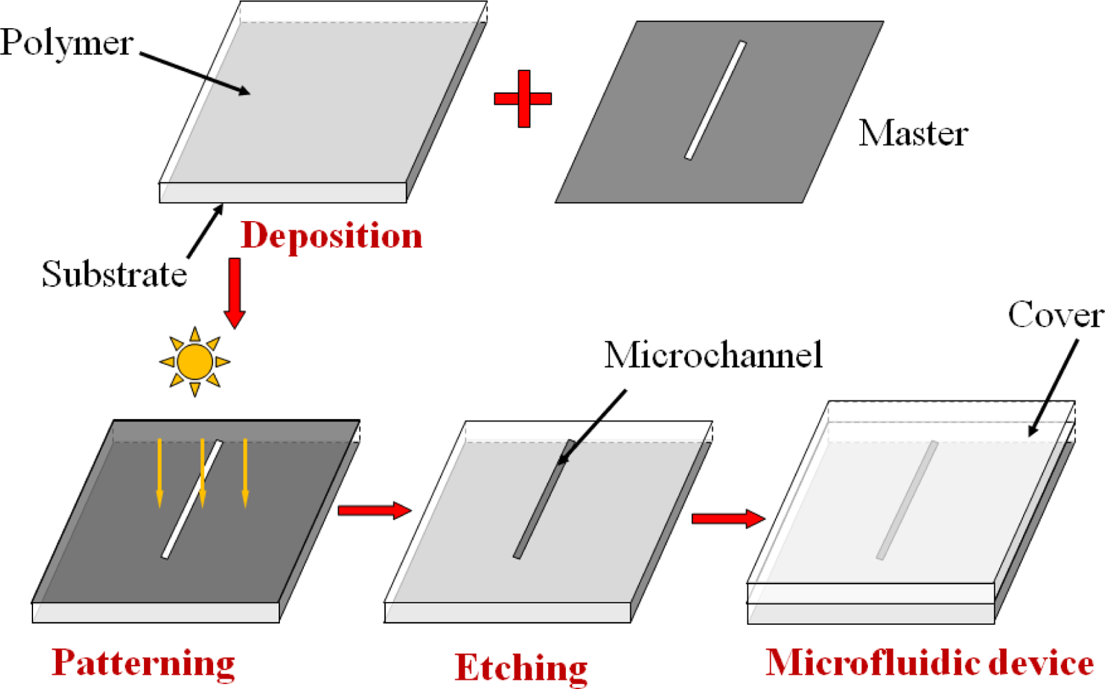
The original microfluidic fabrication technologies were derived from silicon microelectronics, which were well developed in semiconductor industry. However, these techniques are very expensive, complicated, and time consuming. In addition, silicon is not suitable to be applied in a microfluidic device due to its opacification to the visible and UV light in addition to its high cost. Feasible techniques for the fabrication of microfluidic devices include microelectromechanical systems (MEMS) with its procedures illustrated in Figure 1. During the fabrication, a material, especially a polymer, is deposited on a substrate first, and then a pattern in a master is transferred into the material by lithography. After an etching process (wet or dry etching), either the exposed or unexposed material is removed. Finally a cover is attached on the surface of the chip to enclose the microchannels.
Another widely adopted method to fabricate a microfluidic system is casting, in which a soft polymer elastomer of high optical transparency is used, i.e., poly(dimethylsiloxane) (PDMS) or poly(methyl methacrylate) (PMMA). Figure 2 shows the steps for the fabrication of a microfluidic device by casting. A mold is produced by soft lithography [12,13] or laser fabrication [14–16] in a photoresist layer (SU-8) or a metallic sheet. Hot embossing technique [14,16,17] or poured molding method [15,18–20] is used to duplicate the mold in a polymer sheet. The peeled polymer replica is sealed to a flat surface to enclose the channels. Much complex structures in a microfluidic device can be developed by stacking multiple polymer layers (100 μm in thickness per layer), similar to a sandwich structure [18,21]. The time period is less than two days starting from design to the realization of a functional device. A list of materials used in the fabrication of opto-microfluidic devices with different molding fabrication techniques is presented in Table 2, which shows that PDMS is the most popular material used in poured molding method and PMMA is widely used in hot embossing technique. In some cases, optical components, especially optofluidic waveguides, have been integrated into the chips and their effectiveness in the transmission of light has been demonstrated. Examples include solid core/solid cladding waveguides [22,23], solid core/liquid cladding waveguides, liquid core/solid cladding waveguides [24], liquid core/liquid cladding waveguides, and hybrid waveguides [18,25,26].
2.2. Femtosecond Laser Fabrication of Opto-Microfluidic Sensors
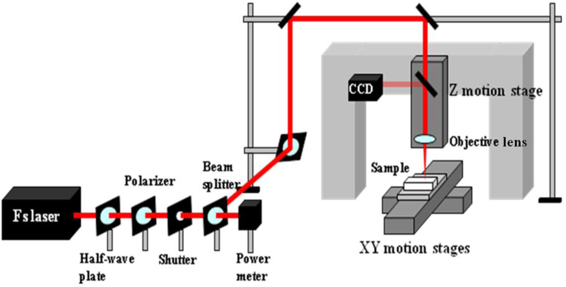
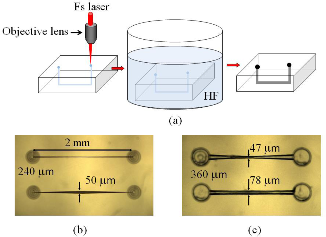
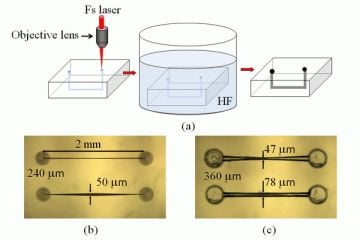
For the applications in optofluidics, the drawbacks of using polymer materials such as solubility in many common solvents, damage upon tightly focused laser irradiation, and fluorescence at certain common wavelengths appear to be severe. In contrast, the glass-based devices with high optical transparency to visible light and inertia to chemical solvents are very suitable for these applications. Consequently, new fabrication techniques are required to realize microfabrication in various glasses. In this regard, ultrafast laser microfabrication, which utilizes ultrashort laser pulses of pulse width as narrow as ∼100 femtoseconds (a femtosecond laser), has been revealed as a powerful approach to fabricate opto-microfluidic devices in glasses [27]. Figure 3 shows a schematic illustration of a home-made femtosecond laser microfabrication station established in our laboratory at the Memorial University of Newfoundland [28]. By shining a piece of glass with a focused femtosecond laser of a peak intensity well above the damage threshold of the glass, three-dimensional microstructures could be generated in the glass. Figure 4 shows a femtosecond-laser-microfabricated microchannel in a fused silica observed by an atomic force microscope (AFM), indicating widths at the top and bottom of the channel of ∼5 and 2 μm, respectively.
After hydrofluoric (HF) acid etching for 3–5 hours, microchannels are generated, which can be adopted in opto-microfluidic devices. The procedures for the fabrication of opto-microfluidic devices with a femtosecond laser are shown in Figure 5(a). Examples of opto-microfluidic channels and microstructures fabricated in our group are shown in Figure 5(b,c).
Compared with MEMS techniques, the ultrafast laser microfabrication possesses salient advantages of simplicity, high efficiency, and versatility. In addition to the fabrication of microchannels, optical waveguides can also be fabricated by an ultrafast laser [29–31]. When a femtosecond laser beam with pulse energy of several hundred nano-Joules is irradiated on the glass, the refractive index of the region in glass will increase. This type of waveguide is called a Type I waveguide. Another type of waveguide, i.e., Type II waveguide, can be fabricated with higher peak energy. Laser irradiation with peak intensity higher than the damage threshold of the glass causes the material at the focus to vaporize, thus the high pressure pushes the material to both sides of the irradiated region. Consequently, the tracks at the two sides result in a higher refractive index while the region between the tracks guides light. In this case, the distance between the two tracks should be shorter than 50 μm. Figure 6 is a Type II waveguide coupling with a He-Ne laser at 633 nm. The propagation loss of this kind of waveguide is ∼4 dB/cm, which is somewhat higher than the values of waveguides fabricated by other techniques. However, the propagation loss in an optical waveguide fabricated by a femtosecond laser could be reduced after optimization of the fabrication parameters including the laser properties. The relatively higher propagation loss does not have a serious effect for the adoption of these waveguides in opto-microfluidic devices.
Table 3 lists a comparison of the properties of some reported optofluidic waveguides fabricated by different techniques. Among three leading fabrication technologies, i.e., MEMS, casting, and femtosecond laser microfabrication, the resultant optofluidic waveguides have quite different light propagation properties. It is important to keep in mind that the propagation loss of a waveguide is relative to the material property of the core and cladding (refractive index) and the carried wavelength. For the waveguides fabricated by MEMS or casting techniques, their core and cladding materials can be either liquid or solid. The reported propagation losses of the waveguides fabricated by MEMS techniques range from 0.5 to 4 dB/cm while the values for the waveguides fabricated by molding fall in a range of 1.8–8.2 dB/cm. The femtosecond laser microfabrication technique is a powerful method to fabricate opto-microfluidic waveguides, in particularly on glasses. With the Type I or II waveguides fabricated with different peak intensities of the lasers, different propagation losses of the waveguides have been achieved, in which values around ∼1 dB/cm were found for the Type I waveguides and slightly higher propagation losses for the Type II waveguides.
Any of the aforementioned microfabrication techniques is effective to fabricate opto-microfluidic devices with pros and cons. Table 4 compares the advantages and drawbacks of different microfabrication techniques used for fabricating opto-microfluidic sensors. Judicious selection is necessary in order to choose a suitable technique for a specific application. In some cases, special approach may be required to overcome the drawbacks of specific microfabrication technique.
3. Applications of Opto-Microfluidic Sensors
3.1. Opto-Microfluidic Sensors for Biological Analysis
The original motivation for developing opto-microfluidics was for biological analysis, in which immunoassay and DNA separation have been the two main applications. Immunoassay is a biochemical technique that detects the presence and quantities of antibodies or antigens in the samples [32–34]. Competitive immunoassay and sandwich assay are two common methods [28]. When a labeled (such as an enzyme or fluorescent dye) analytical reagent with special antigens or antibodies is mixed with the sample, a specific binding will form between the antigen and the corresponding antibody. The changes in the color and intensity of light from the labeled binding are recorded to identify the immunity of the sample. The traditional technique requires a large amount of reagents and a long incubation time. Microfluidics-based immunoassays have been developed by several research groups. For instance, in a sandwich assay for antigen, antibody is injected into the microchannels by pressure-driven [35], electrokinetic control [36,37] or centrifugal force [38], and deposited onto the wall of the microchannels to form solid-phase antibody, then antigen in the sample is mixed with solid-phase antibody in the microchannel, and finally another labeled antibody is added for signal generation. The color signals from the antibody-antigen-labeled antibody bindings are detected by a fluorescence microscope after removing excess antibodies and antigens through washing steps. All steps can be completed in one hour, and the reagent consumption is only on the order of microliters. Roos et al. [39] and Herrmann et al. [40] used microspheres to support the binding, and the fluorescence signals were collected from these microbeads. These microspheres provided increased surface area to support the immune complex. Nanoparticle-labeled microfluidic immunoassay [41] was reported by Lin et al., in which free labeled antigens were deposited on the nanoscaled gold particles and the scattered light from the particles provided readout to trace the bindings between antibodies and antigens.
As a prerequisite step to allow opto-microfluidic measurement, capillary electrophoresis (CE) is a rapidly growing separation technique, which has been applied in bioanalysis, environmental pollutant analysis and food analysis [42,43]. By using high electric fields (larger than 500 V/cm), buffer solution and all ions, positive or negative particles in the sample generate electroosmotic and electrophoretic flow respectively. Electroosmotic flow pulls the analytes in the buffer solution through the capillary toward the cathode. However, the electrophoretic flow reduces the flow rate of the negatively charged analytes and increases the flow rate of positively charged analytes in the capillary. Therefore, the analytes separate due to different mobilities. Ultraviolet (UV) absorption detectors are equipped to detect the ingredients of the sample near the outlet of the capillary. The data from the detector is displayed as an electropherogram, in which peaks at different times are shown for separated chemical compounds.
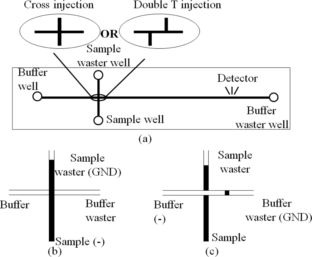
A CE instrument is formed after assembling the microchannels and reservoirs in a chip with extra high potential. Figure 7 illustrates two types of CE chips and their operations. The CE chips are extensively used in medical research such as DNA analysis [44], infectious disease diagnostics [45] and sample purification [46]. Now some companies such as Micronit Microfluidics BV in The Netherlands, microLIQUID in USA, and Micralyne Inc. in Canada supply CE chips and kits for clinical diagnostics. Meanwhile, several research groups have integrated different components into the CE chips to satisfy diverse needs of analysis. For example, combination of polymerase chain reaction (PCR) with CE chip (PCR-CE chip) is a focus of research, in which one or multiple PCR chambers are integrated into the CE chip to incubate and analyze DNA simultaneously [47–52]. Prakash et al. fabricated PCR arrays on the CE chip with two PCR valves and ports to control the flow of samples in each PCR chamber, so that the CE chip can be reusable without contamination [53]. CE chips integrated with multichannels for mixing, reaction and separation were also reported by some Canadian research groups [54–57]. Munce et al. used CE with optical tweezers to achieve single-cell sorting and analysis in one chip [58]. A CE chip with an acoustic wave sensor successfully trapped one live myocyte in the acoustic wave sensor region [59], in which the contraction and relaxation of the cell were clearly detected without the influence from other cells.
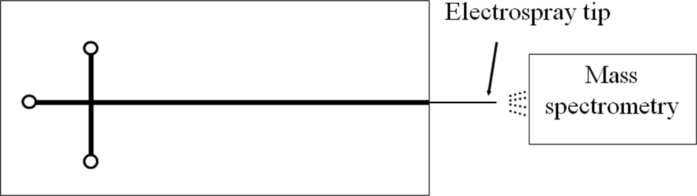
The commonly adopted detection method in a CE chip is a confocal detective system. Bliss et al. integrated optical waveguides into a CE chip [60]. However, the electropherogram demonstrated that the waveguide detection possesses an equal or greater sensitivity than that of the confocal system. A good technique to accurately identify the ingredient of a sample is to connect the outlet of the capillary to an electrospray mass spectrometry (ESMS) [52], as shown in Figure 8.
3.2. Opto-Microfluidic Chemical Sensors
Polymer particles are highly sought in biology, cosmetics, food process, medicine, and pesticide. However, the incomplete control and high cost of traditional chemical synthesis techniques limit their applications. One research group at the University of Toronto proposed a novel approach to realize continuous and scalable production of core-shell droplets and polymer capsules in microfluidic devices in 2005 [61]. Two or more different kinds of immiscible liquids were infused into a microfluidic device and the mixed liquid flew through a thin “focused” orifice. Different core-shell droplets were synthesized by changing the liquid flow rates, which were controlled by push pumps. UV lamp irradiation made the photopolymerizable droplets solidification when droplets flew along a long wavy microchannel. Polymer particles were then obtained at the output of the device. This technique could precisely control the sizes of the particles, liquid cores, shells, and the number of core droplets. During the subsequent years, further research had been carried out by the same group to address additional topics, such as biopolymer microcapsules [62], Janus and ternary particles [63], microgels of biological polymers [64], monodisperse particles with microspheres, rods, disks and ellipsoids [65], dynamic lattices [66,67], and colloidal particles at gas–liquid interfaces [68]. This kind of chemical sensors could better explore the dynamics and mechanisms of physical and chemical reactions which are difficult to be investigated in conventional experiments.
Centrifugal microfluidic devices were reported by a research group at McGill University, in which multiple chambers and capillary valves were fabricated in a disc. The flow of the solvent was controlled to achieve dissolution [69], mixing [70], extraction [21,71] and reaction [70] between reagents by adjusting the rotational rate of the disc. The components and concentrations of analytes were measured at the detection unit by fluorescence and absorption spectra. In some cases, magnets were utilized in the chamber and base to serve as an agitator to increase the efficiency of chemical reaction. The centrifugal microfluidic devices could be applied in environmental monitoring and soil analysis for their portability and rapidity.
Optofluidic platform for chemical component analysis by laser-induced breakdown spectroscopy (LIBS) was achieved by a research group at the University of Alberta [72,73]. A small thermal or piezoelectric actuator was deposited on the bottom of a microchannel while an orifice of a few microns was opened on the opposite wall of the actuator. During the operation, a bubble was first excited at the orifice by the actuator, and then a fast intense laser pulse broke down the bubble, and thus plasma with the components of reagent was generated. As the plasma was cooled down, electrons and ions were recombined, accompanied by emitting electromagnetic radiation with fingerprint wavelengths of the elements in the reagent, which was detected by its spectroscopy. The most notable advantage of this technique is the non-contact measurement, which completely avoids sample contamination.
3.3. Opto-Microfluidic Surface Plasmon Resonance Sensors
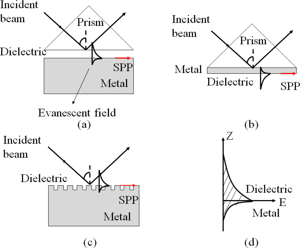
Surface plasmon polaritons (SPP) are electromagnetic waves that propagate along a metal and dielectric interface [74,75]. SPP can be evanescent, which are excited by both electrons and photons. The excitation of SPP by photons is usually referred as surface plasmon resonance (SPR). SPP cannot be directly excited by photons due to momentum mismatch. Special arrangements, such as Otto configuration [76], Kretschmann configuration [77], or a diffraction grating [78], are well-known techniques to couple photons into SPP in order to match the wave vectors of the photon and the surface plasmon, as illustrated in Figure 9. The Kretschmann configuration is the most common approach, in which the thickness of the metal layer is usually a few tens of nanometers to ensure the evanescent wave to travel through the metal and couple to a surface plasmon mode, which is shown in Figure 9(d).
Since the wave travels on the interface of the metal and the external dielectric layer, SPR is very sensitive to any change at this interface, such as the density and temperature of the dielectric layer and the structure of the metal surface. Opto-microfluidic SPR sensors for immunoassay and refractive index measurement have been demonstrated. Chien et al. integrated SPR into a microfluidic platform [79], in which diffractive mirrors were attached on the prism to focus the incident light in the direction of wave vectors while liquid solution as the dielectric material was infused into a gold-coated microchannel. When light with different incident angles is irradiated on the surface of the prism and metal, part of the light, which matches with the SPR angle θSP, is attenuated into the metal to generate SPR and the rest of the light is reflected. A photodetector can be placed at the end of the device to capture and monitor the intensity of the reflected wave. The reflected light of reduced intensity at the SPR angle would be detected due to the optical absorption by the metal. The sensor has been proved to be effective in measuring refractive indices of liquids by monitoring changes in the SPR angles with NaCl solution as a testing material.
Nanohole based SPR sensors have received considerable attention in recent years. One of the most important characteristics of a nanohole array is that the intensities of the transmitted light enhance at certain wavelengths due to the SPP coupling when the incident light irradiates on the surface of the metal film. By monitoring the wavelengths of the intensity peaks, a nanohole-based SPR sensor is realized. Compared with a standard reflective mode SPR sensor, a nanohole SPR sensor operates at the normal incidence without the necessity to consider the SPP angle. Sinton group at the University of Victoria realized nanohole array SPR sensors [80–85]. For example, a device with flow-through nanohole arrays, instead of dead-ended nanohole arrays in a SPR sensor, could make the regents to travel through the nanoholes rapidly, thus reducing the response time remarkably [85].
With the improvement of SPR techniques, surface plasmon resonance imaging (SPRI) has been proposed as a new kind of detection technique in biology [86]. Kanda et al. at the University of Alberta patterned a surface of metal (gold) with free-labeled protein antigens arrays [87]. When the sample flew through the microchannel located above the patterned gold film, the antigen-antibody bindings were generated at the arrays. A high contrast SPRI based on the adsorbed proteins was realized to evaluate the quantitative and qualitative properties of the antibodies in the sample. Tabrizian group at the McGill University replaced the plain gold film in the SPR with periodic gold nanoposts to detect DNA hybridization. The optimal result showed a fivefold SPRI enhancement compared with the common SPRI [88]. This group also combined SPRI technique with digital microfluidics (DMF) to detect biological samples [89,90]. DMF is a fluid manipulation technique, in which a patterned array of electrodes is etched on the substrate with MEMS techniques and then coated with a waterproof material like Teflon to form the DMF. Droplets can dispense and merge in the DMF when an electrical potential is applied on sequential electrodes in the array [91–95]. Therefore, this combination realized real-time monitoring and detection of reaction occurring as required.
3.4. Opto-Microfluidic Sensors Integrated with Novel Optical Functionalities
Integrating micro-optical components into a chip could effectively shape beams to enhance the sensitivity of a sensor and increase its portability. Besides optical waveguides discussed in the previous sections, Table 5 lists several micro-optical components integrated in opto-microfluidic devices, which include lenses [96,97], gratings [22,98], mirrors [79,99], and light sources [100,101]. There is continuing effort to realize integration of multiple components to acquire novel optical functionalities.
Optical tweezers are important instruments to trap and sort particles like cells, proteins, and microspheres. A tightly-focused laser beam (Gaussian beam) provides an attractive or repulsive force on the particles due to the changes in the momentum of light upon reflection or refraction. Although the force is on the order of piconewtons, it is large enough to hold and move small objects with sizes of several tens of microns. Taking advantages of the merits of opto-microfluidic devices with narrow channel widths, fiber-microfluidic tweezers have been particularly attractive in studying a variety of biological systems. Sinton group realized trapping microsphere array by dual-beam with a focus on the study of optohydrodynamics and optical interactions between particles, which could be applied for contact-free storage of biological cells as well [102–105]. In addition, Guo et al. at the University of Ottawa fabricated a microfluidic chip with on-chip lens structures to reduce the beam waist of the light and achieved a higher efficiency in optical operation and optofluidic transportation [96].
Microcytometer is another important application of opto-microfluidic sensors. Azmayesh-Fard et al. [18] coupled excitation lasers of different wavelengths into the microfluidic devices by solid-core waveguides and different dyed particles could be resolved from different peaks after a windowed Fourier transform to output signals. Multiple parallel waveguides were integrated into an opto-microfluidic sensor to collect the fluorescent and scattered signals from the labeled cells by Xu group in McMaster University [106]. The same group also fabricated micro-lenses in the chips to shape the excitation beam and improve the signal-to-noise ratio of cytometers [97]. A wide-angle microfluidic cytometer was reported by a research group at the University of Alberta [107–109]. A conventional cytometer can only collect signals through small-angle forward scattering (5°) and side scattering (10°) in which errors are apparent when cells gather or irregular cells and other organelles exist. In the wide-angle microfluidic cytometer, the goniometric measurement and finite-difference time-domain (FDTD) method were adopted to overcome the disadvantages of the conventional cytometers.
Refractive index (RI) sensing is another important application of opto-microfluidic sensors, which have been widely applied in environmental monitoring and optical measurement. Opto-microfluidic RI sensors based on Mach-Zehnder interferometer (MZI) [23,110,111], grating [98,112], and refractometer [99] have been reported by several research groups in Canada. All these reported methods adopted similar principles in which two identical beams were first coupled into different paths such as a solid core waveguide or a liquid core waveguide, then interference occurred due to the difference in the optical paths when the two beams were combined together. The measurement of the refractive index of the liquid can be achieved by monitoring the change of the interference intensity.
4. Conclusions
Research on opto-microfluidics has achieved significant progress over recent years. Considering some successful microfluidic devices and systems, optofluidics is a field still in its infancy with plenty room for further development and promising applications. With the development of advanced microfabrication techniques, more advanced opto-microfluidic sensors with increased functionalities and compactness will be developed. One important aspect for further investigation is on the integration of microfluidic platforms and fluid actuation techniques to allow efficient interactions with optical signals. One the other hand, optical components and mechanisms are crucial to achieve optical control of fluids. An enhanced understanding of the interplay between optics and fluids will make it possible to realize reconfigurable optical systems with novel functionalities. Discoveries in other research fields will benefit the development of opto-microfluidics. For example, smaller waveguide (nano-waveguide or sub-wavelength waveguide) or nanofluidics will be interesting for realizing nanodevices and nanosystems with higher integration density. Significant achievement is anticipated through extensive collaborations among researchers from different disciplines as well as from different countries and regions to address topics in this interdisciplinary field.
Acknowledgments
This work has been supported by the Natural Sciences and Engineering Research Council of Canada (NSERC), the Canada Research Chairs Program, the Canada Foundation for Innovation, the Province of Newfoundland and Labrador, and the Memorial University of Newfoundland.
References
- Terry, SC; Jerman, JH; Angell, JB. A gas chromatographic air analyzer fabricated on a silicon wafer. IEEE Trans. Electron. Dev 1979, 26, 1880–1886. [Google Scholar]
- Whitesides, GM. The origins and the future of microfluidics. Nature 2006, 442, 368–373. [Google Scholar]
- Nguyen, NT; Wereley, ST. Fundamentals and Applications of Microfluidics, 2nd ed; Artech House: Norwood, MA, USA, 2006. [Google Scholar]
- Colin, S. Microfluidics; Wiley: Hoboken, NJ, USA, 2010. [Google Scholar]
- Zhu, H; White, IM; Suter, JD; Dale, PS; Fan, X. Analysis of biomolecule detection with optofluidic ring resonator sensors. Opt. Express 2007, 15, 9139–9146. [Google Scholar]
- Lu, P; Men, L; Sooley, K; Chen, Q. Tapered fiber Mach-Zehnder interferometer for simultaneous measurement of refractive index and temperature. Appl. Phys. Lett 2009, 94, 131110. [Google Scholar]
- Liang, W; Huang, Y; Xu, Y; Lee, RK; Yariv, A. Highly sensitive fiber Bragg grating refractive index sensors. Appl. Phys. Lett 2005, 86, 151122. [Google Scholar]
- Lu, P; Chen, Q. Femtosecond laser microstructured fibre refractive index sensor with temperature compensation. Elect. Lett 2010, 46, 1616–2617. [Google Scholar]
- Fainman, Y; Lee, LP; Psaltis, D; Yang, C. Optofluidics: Fundamentals, Devices, and Applications; McGraw-Hill: New York, NY, USA, 2010. [Google Scholar]
- Psaltis, D; Quake, RS; Yang, C. Developing optofluidic technology through the fusion of microfluidics and optics. Nature 2006, 442, 381–386. [Google Scholar]
- Monat, C; Domachuk, P; Eggleton, BJ. Integrated optofluidics: A new river of light. Nat. Photon 2007, 1, 106–114. [Google Scholar]
- Koerner, T; Brown, L; Xie, R; Oleschuk, RD. Epoxy resins as stamps for hot embossing of microstructures and microfluidic channels. Sens. Actuat. B 2005, 107, 632–639. [Google Scholar]
- Ssenyange, S; Taylor, J; Harrison, DJ; McDermott, MT. A glassy carbon microfluidic device for electrospray mass spectrometry. Anal. Chem 2004, 76, 2393–2397. [Google Scholar]
- Shiu, PP; Knopf, GK; Ostojic, M; Nikumb, S. Rapid fabrication of tooling for microfluidic devices via laser micromachining and hot embossing. J. Micromech. Microeng 2008, 18, 025012. [Google Scholar]
- Shiu, PP; Knopf, GK; Ostojic, M; Nikumb, S. Rapid fabrication of micromolds for polymeric microfluidic devices. Proceedings of Canadian Conference of Electrical and Computer Engineering, Vancouver, BC, Canada, 22–26 April 2007; pp. 8–11.
- Shiu, PP; Knopf, GK; Ostojic, M; Nikumb, S. Fabrication of polymer microfluidic devices with 3D microfeatures that have near optical surface quality. Proceedings of Microsystems and Nanoelectronics Research Conference, Ottawa, ONT, Canada, 15 October 2008; pp. 53–56.
- Cameron, NS; Roberge, H; Veres, T; Jakeway, SC; Crabtree, HJ. High fidelity, high yield production of microfluidic devices by hot embossing lithography: Rheology and stiction. Lab Chip 2006, 6, 936–941. [Google Scholar]
- Azmayesh-Fard, SM; Flaim, E; McMullin, JN. PDMS biochips with integrated waveguides. J. Micromech. Microeng 2010, 20, 087002. [Google Scholar]
- Wang, B; Abdulali-Kanji, Z; Dodwell, E; Horton, JH; Oleschuk, RD. Surface characterization using chemical force microscopy and the flow performance of modified polydimethylsiloxane for microfluidic device applications. Electrophoresis 2003, 24, 1442–1450. [Google Scholar]
- Subramani, BG; Selvaganapathy, PR. Surface micromachined PDMS microfluidic devices fabricated using a sacrificial photoresist. J. Micromech. Microeng 2009, 19, 015013. [Google Scholar]
- Xi, Y; Duford, DA; Salin, ED. Automated liquid-solid extraction of pyrene from soil on centrifugal microfluidic devices. Talanta 2010, 82, 1072–1076. [Google Scholar]
- Bock, PJ; Cheben, P; Schmid, JH; Lapointe, J; Delâge, A; Janz, S; Aers, GC; Xu, D; Densmore, A; Hall, TJ. Subwavelength grating periodic structures in silicon-on-insulator: A new type of microphotonic waveguide. Opt. Express 2010, 18, 20251–20262. [Google Scholar]
- Dumais, P; Callender, CL; Noad, JP; Ledderhof, CJ. Integrated optical sensor using a liquid-core waveguide in a Mach-Zehnder interferometer. Opt. Express 2008, 16, 18164–18172. [Google Scholar]
- Bliss, CL; McMullin, JN; Backhouse, CJ. Integrated wavelength-selective optical waveguides for microfluidic-based laser-induced fluorescence detection. Lab Chip 2008, 8, 143–151. [Google Scholar]
- Densmore, AD; Xu, X; Janz, S; Waldron, P; Lapointe, J; Mischki, T; Lopinski, G; Delage, A; Schmid, JH; Cheben, P. Sensitive label-free biomolecular detection using thin silicon waveguides. Adv Opt Technol.
- Kowpak, T; Watts, BR; Zhang, Z; Zhu, S; Xu, C. Fabrication of photonic/microfluidic integrated devices using an epoxy photoresist. Macromol. Mater. Eng 2010, 295, 559–565. [Google Scholar]
- Zheng, HY; Liu, H; Wan, S; Lim, GC; Nikumb, S; Chen, Q. Ultrashort pulse laser micromachined microchannels and their application in an optical switch. Int. J. Adv. Manuf. Technol 2006, 27, 925–929. [Google Scholar]
- Lu, P; Chen, Q. Femtosecond laser microfabricated fiber Mach-Zehnder interferometer for sensing applications. Opt. Lett 2011, 36, 268–270. [Google Scholar]
- Zhang, H; Ho, S; Eaton, SM; Li, J; Herman, PR. Three-dimensional optical sensing network written in fused silica glass with femtosecond laser. Opt. Express 2008, 16, 14015–14023. [Google Scholar]
- Shah, L; Arai, AY; Eaton, SM; Herman, PR. Waveguide writing in fused silica with a femtosecond fiber laser at 522 nm and 1 MHz repetition rate. Opt. Express 2005, 13, 1999–2006. [Google Scholar]
- Nejadmalayeri, AH; Herman, PR; Burghoff, J; Will, M; Nolte, S; Tünnermann, A. Inscription of optical waveguides in crystalline silicon by mid-infrared femtosecond laser pulses. Opt. Lett 2005, 30, 964–966. [Google Scholar]
- Blake, C; Gould, BJ. Use of enzymes in immunoassay techniques. A review. Analyst 1984, 109, 533–546. [Google Scholar]
- Wild, D. The Immunoassay Handbook, 3rd ed; Elsevier: Oxford, UK, 2008. [Google Scholar]
- Mikkelsen, SR; Corton, E. Bioanalytical Chemistry; Wiley: Hoboken, NJ, USA, 2004. [Google Scholar]
- Lin, FYH; Sabri, M; Erickson, D; Alirezaie, J; Li, D; Sherman, PM. Development of a novel microfluidic immunoassay for the detection of Helicobacter pylori infection. Analyst 2004, 129, 823–828. [Google Scholar]
- Gao, Y; Lin, FYH; Hu, G; Sherman, PM; Li, D. Development of a novel electrokinetically driven microfluidic immunoassay for the detection of Helicobacter pylori. Anal. Chim. Acta 2005, 543, 109–116. [Google Scholar]
- Xiang, Q; Hu, G; Gao, Y; Li, D. Miniaturized immunoassay microfluidic system with electrokinetic control. Biosens. Bioelectron 2006, 21, 2006–2009. [Google Scholar]
- Peytavi, R; Raymond, FR; Gagné, D; Picard, J; Jia, G; Zoval, J; Madou, M; Boissinot, K; Boissinot, M; Bissonnette, L; Ouellette, M; Bergeron, MG. Microfluidic device for rapid (<15 min) automated microarray hybridization. Clin. Chem 2005, 51, 1836–1844. [Google Scholar]
- Roos, P; Skinner, CD. A two bead immunoassay in a micro fluidic device using a flat laser intensity profile for illumination. Analyst 2003, 128, 527–531. [Google Scholar]
- Herrmann, M; Veresb, T; Tabrizian, M. Enzymatically-generated fluorescent detection in micro-channels with internal magnetic mixing for the development of parallel microfluidic ELISA. Lab Chip 2006, 6, 555–560. [Google Scholar]
- Lin, FYH; Sabri, M; Alirezaie, J; Li, D; Sherman, PM. Development of a nanoparticle-labeled microfluidic immunoassay for detection of pathogenic microorganisms. Clin. Diagn. Lab Immunol 2005, 12, 418–425. [Google Scholar]
- Schmitt-Kopplin, P; Munchen, H. Capillary Electrophoresis: Methods and Protocols; Humana Press: Totowa, NJ, USA, 2008. [Google Scholar]
- Skoog, DA; Holler, FJ; Crouch, SR. Principles of Instrumental Analysis, 6th ed; Thomson Brooks/Cole: Belmont, CA, USA, 2007. [Google Scholar]
- Taylor, P; Managea, DP; Helmle, KE; Zheng, Y; Glerum, DM; Backhouse, CJ. Analysis of mitochondrial DNA in microfluidic systems. J. Chromatogr. B 2005, 822, 78–84. [Google Scholar]
- Klostranec, JM; Xiang, Q; Farcas, GA; Lee, JA; Rhee, A; Lafferty, EI; Perrault, SD; Kain, KC; Chan, WCW. Convergence of quantum dot barcodes with microfluidics and signal processing for multiplexed high-throughput infectious disease diagnostics. Nano Lett 2007, 7, 2812–2818. [Google Scholar]
- Footz, T; Wunsam, S; Kulak, S; Crabtree, HJ; Glerum, DM; Backhouse, CJ. Sample purification on a microfluidic device. Electrophoresis 2001, 22, 3868–3875. [Google Scholar]
- Pilarski, LM; Lauzon, J; Strachan, E; Adamia, S; Atrazhev, A; Belch, AR; Backhouse, CJ. Sensitive detection using microfluidics technology of single cell PCR products from high and low abundance IgH VDJ templates in multiple myeloma. J. Immunol. Method 2005, 305, 94–105. [Google Scholar]
- Chowdhury, J; Kagiala, GV; Pushpakom, S; Lauzon, J; Makin, A; Atrazhev, A; Stickel, A; Newman, WG; Backhouse, CJ; Pilarski, LM. Microfluidic platform for single nucleotide polymorphism genotyping of the thiopurine s-methyltransferase gene to evaluate risk for adverse drug events. J. Mol. Diagn 2007, 9, 521–529. [Google Scholar]
- van Dijken, J; Kaigala, GV; Lauzon, J; Atrazhev, A; Adamia, S; Taylor, BJ; Reiman, T; Belch, AR; Backhouse, CJ; Pilarski, LM. Microfluidic chips for detecting the t(4;14) translocation and monitoring disease during treatment using reverse transcriptase-polymerase chain reaction analysis of IgH-MMSET hybrid transcripts. J. Mol. Diagn 2007, 9, 358–367. [Google Scholar]
- Prakash, AR; Rosa, CDL; Fox, JD; Kaler, KVIS. Identification of respiratory pathogen Bordetella Pertussis using integrated microfluidic chip technology. Microfluid. Nanofluid 2008, 4, 451–456. [Google Scholar]
- Kaigala, GV; Huskins, RJ; Preiksaitis, J; Pang, X; Pilarski, LM; Backhouse, CJ. Automated screening using microfluidic chip-based PCR and product detection to assess risk of BK virus-associated nephropathy in renal transplant recipients. Electrophoresis 2006, 27, 3753–3763. [Google Scholar]
- Wang, C; Oleschuk, R; Ouchen, F; Li, J; Thibault, P; Harrison, DJ. Integration of immobilized trypsin bead beds for protein digestion within a microfluidic chip incorporating capillary electrophoresis separations and an electrospray mass spectrometry interface. Rapid Commun. Mass Spectrom 2000, 14, 1377–1383. [Google Scholar]
- Prakash, R; Kaler, KVIS. An integrated genetic analysis microfluidic platform with valves and a PCR chip reusability method to avoid contamination. Microfluid. Nanofluid 2007, 3, 177–187. [Google Scholar]
- Chiem, N; Colyer, C; Harrison, DJ. Microfluidic systems for clinical diagnostics. Proceedings of International Conference on Solid-State Sensors and Actuators, Chicago, IL, USA, 16–19 June 1997; 1, pp. 183–186.
- Qiu, CX; Harrison, DJ. Integrated self-calibration via electrokinetic solvent proportioning for microfluidic immunoassays. Electrophoresis 2001, 22, 3949–3958. [Google Scholar]
- Tang, T; Badal, MY; Ocvirk, G; Lee, WE; Bader, DE; Bekkaoui, F; Harrison, DJ. Integrated microfluidic electrophoresis system for analysis of genetic materials using signal amplification methods. Anal. Chem 2002, 74, 725–733. [Google Scholar]
- Cheng, SB; Skinner, CD; Taylor, J; Attiya, S; Lee, WE; Picelli, G; Harrison, DJ. Development of a multichannel microfluidic analysis system employing affinity capillary electrophoresis for immunoassay. Anal. Chem 2001, 73, 1472–1479. [Google Scholar]
- Munce, NR; Li, JZ; Herman, PR; Lilge, L. Microfabricated system for parallel single-cell capillary electrophoresis. Anal. Chem 2004, 76, 4983–4989. [Google Scholar]
- Li, PCH; Wang, W; Parameswaran, M. An acoustic wave sensor incorporated with a microfluidic chip for analyzing muscle cell contraction. Analyst 2003, 128, 225–231. [Google Scholar]
- Bliss, CL; McMullin, JN; Backhouse, CJ. Rapid fabrication of a microfluidic device with integrated optical waveguides for DNA fragment analysis. Lab Chip 2007, 7, 1280–1287. [Google Scholar]
- Nie, Z; Xu, S; Seo, M; Lewis, PC; Kumacheva, E. Polymer particles with various shapes and morphologies produced in continuous microfluidic reactors. J. Am. Chem. Soc 2005, 127, 8058–8063. [Google Scholar]
- Zhang, H; Tumarkin, E; Peerani, R; Nie, Z; Sullan, RMA; Walker, GC; Kumacheva, E. Microfluidic production of biopolymer microcapsules with controlled morphology. J. Am. Chem. Soc 2006, 128, 12205–12210. [Google Scholar]
- Nie, Z; Li, W; Seo, M; Xu, S; Kumacheva, E. Janus and ternary particles generated by microfluidic synthesis: Design, synthesis, and self-assembly. J. Am. Chem. Soc 2006, 128, 9408–9412. [Google Scholar]
- Zhang, H; Tumarkin, E; Sullan, RMA; Walker, GC; Kumacheva, E. Exploring microfluidic routes to microgels of biological polymers. Macromol. Rapid Commun 2007, 28, 527–538. [Google Scholar]
- Xu, S; Nie, Z; Seo, M; Lewis, P; Kumacheva, E; Stone, HA; Garstecki, P; Weibel, DB; Gitlin, I; Whitesides, GM. Generation of monodisperse particles by using microfluidics: Control over size, shape, and composition. Angew. Chem 2005, 117, 734–738. [Google Scholar]
- Seo, M; Nie, Z; Xu, S; Lewis, PC; Kumacheva, E. Microfluidics: From dynamic lattices to periodic arrays of polymer disks. Langmuir 2005, 21, 4773–4775. [Google Scholar]
- Seo, M; Paquet, C; Nie, Z; Xua, S; Kumacheva, E. Microfluidic consecutive flow-focusing droplet generators. Soft Matter 2007, 3, 986–992. [Google Scholar]
- Park, JI; Nie, Z; Kumacheva, A; Abdelrahman, AI; Binks, BP; Stone, HA; Kumacheva, E. A microfluidic approach to chemically driven assembly of colloidal particles at gas-liquid interfaces. Angew. Chem 2009, 121, 5404–5408. [Google Scholar]
- Duford, DA; Peng, DD; Salin, ED. Magnetically driven solid sample preparation for centrifugal microfluidic devices. Anal. Chem 2009, 81, 4581–4584. [Google Scholar]
- Xi, Y; Templeton, EJ; Salin, ED. Rapid simultaneous determination of nitrate and nitrite on a centrifugal microfluidic device. Talanta 2010, 82, 1612–1615. [Google Scholar]
- Lafleur, JP; Rackov, AA; McAuley, S; Salin, ED. Miniaturised centrifugal solid phase extraction platforms for in-field sampling, pre-concentration and spectrometric detection of organic pollutants in aqueous samples. Talanta 2010, 81, 722–726. [Google Scholar]
- Godwal, Y; Kaigala, G; Hoang, V; Lui, SL; Backhouse, C; Tsui, YY; Fedosejevs, R. Elemental analysis using micro laser-induced breakdown spectroscopy in a microfluidic platform. Opt. Express 2008, 16, 12435–12445. [Google Scholar]
- Godwal, Y; Taschuk, MT; Lui, SL; Tsui, YY; Fedosejevs, R. Development of laser-induced breakdown spectroscopy for microanalysis applications. Laser Part. Beams 2008, 26, 95–104. [Google Scholar]
- Maier, SA. Plasmonics: Foundamentals and Applications; Springer: New York, NY, USA, 2007. [Google Scholar]
- Welford, K. Surface plasmon-polaritons and their uses. Opt. Quant. Electron 1991, 23, 1–27. [Google Scholar]
- Akowuah, EK; Gorman, T; Haxha, S. Design and optimization of novel surface plasmon resonance biosensor based on Otto configuration. Opt. Express 2009, 17, 23511–23521. [Google Scholar]
- Leong, H-S; Guo, J; Lindquist, RG; Liu, QH. Surface plasmon resonance in nanostructured metal films under the Kretschmann configuration. J. Appl. Phys 2009, 106, 124314. [Google Scholar]
- Yeh, W-H; Kleingartner, J; Hillier, AC. Wavelength tunable surface plasmon resonance—enhanced optical transmission through a chirped diffraction grating. Analyt. Chem 2010, 82, 4988–4993. [Google Scholar]
- Chien, W; Khalid, MZ; Hoa, XD; Kirk, AG. Monolithically integrated surface plasmon resonance sensor based on focusing diffractive optic element for optofluidic platforms. Sens. Actuat. B 2009, 138, 441–445. [Google Scholar]
- Sinton, D; Gordon, R; Brolo, AG. Nanohole arrays in metal films as optofluidic elements: Progress and potential. Microfluid. Nanofluid 2008, 4, 107–116. [Google Scholar]
- Escobedo, C; Brolo, AG; Gordon, R; Sinton, D. Optofluidic sieving with flow-through plasmonic nanohole arrays. Proceedings of Conference of Lasers and Electro-Optics (CLEO) and Quantum Electronics and Laser Science Conference (QELS), San Jose, CA, USA, 16–21 May 2010; pp. 1–2.
- Leebeeck, AD; Kumar, LKS; Lange, V; Sinton, D; Gordon, R; Brolo, AG. On-chip surface-based detection with nanohole arrays. Anal. Chem 2007, 79, 4094–4100. [Google Scholar]
- Eftekhari, F; Gordon, R; Ferreira, J; Brolo, AG; Sinton, D. Polarization-dependent sensing of a self-assembled monolayer using biaxial nanohole arrays. Appl. Phys. Lett 2008, 92, 253103–253106. [Google Scholar]
- Ferreira, J; Santos, MJL; Rahman, MM; Brolo, AG; Gordon, R; Sinton, D; Girotto, EM. Attomolar protein detection using in-hole surface plasmon resonance. J. Am. Chem. Soc 2009, 131, 436–437. [Google Scholar]
- Eftekhari, F; Escobedo, C; Ferreira, J; Duan, X; Girotto, EM; Brolo, AG; Gordon, R; Sinton, D. Nanoholes as nanochannels: Flow-through plasmonic sensing. Anal. Chem 2009, 81, 4308–4311. [Google Scholar]
- Ouellet, E; Lausted, C; Lin, T; Yang, CWT; Hood, L; Lagally, ET. Parallel microfluidic surface plasmon resonance imaging arrays. Lab Chip 2010, 10, 581–588. [Google Scholar]
- Kanda, V; Kariuki, JK; Harrison, DJ; McDermott, MT. Label-free reading of microarray-based immunoassays with surface plasmon resonance imaging. Anal. Chem 2004, 76, 7257–7262. [Google Scholar]
- Malic, L; Cui, B; Veres, T; Tabrizian, M. Enhanced surface plasmon resonance imaging detection of DNA hybridization on periodic gold nanoposts. Opt. Lett 2007, 32, 3092–3094. [Google Scholar]
- Malic, L; Veres, T; Tabrizian, M. Two-dimensional droplet-based surface plasmon resonance imaging using electrowetting-on-dielectric microfluidics. Lab Chip 2009, 9, 473–475. [Google Scholar]
- Malic, L; Veres, T; Tabrizian, M. Biochip functionalization using electrowetting-on-dielectric digital microfluidics for surface plasmon resonance imaging detection of DNA hybridization. Biosens. Bioelectron 2009, 24, 2218–2224. [Google Scholar]
- Watson, MWL; Abdelgawad, M; Ye, G; Yonson, N; Trottier, J; Wheeler, AR. Microcontact printing-based fabrication of digital microfluidic devices. Anal. Chem 2006, 78, 7877–7885. [Google Scholar]
- Abdelgawad, M; Wheeler, AR. Rapid prototyping in copper substrates for digital microfluidics. Adv. Mater 2007, 19, 133–137. [Google Scholar]
- Abdelgawad, M; Wheeler, AR. Low-cost, rapid-prototyping of digital microfluidics devices. Microfluid. Nanofluid 2008, 4, 349–355. [Google Scholar]
- Brassard, D; Malic, L; Normandin, F; Tabrizian, M; Veres, T. Improving the operation of electrowetting-based digital micro-fluidic systems by using water-oil core-shell droplets. Proceedings of the Twelfth International Conference on Miniaturized Systems for Chemistry and Life Sciences, San Diego, CA, USA, 12–16 October 2008; pp. 772–774.
- Luk, VN; Mo, GC; Wheeler, AR. Pluronic additives: A solution to sticky problems in digital microfluidics. Langmuir 2008, 24, 6382–6389. [Google Scholar]
- Guo, H; Zhao, P; Xiao, G; Zhang, Z; Yao, J. Optical manipulation of microparticles in an SU-8/PDMS hybrid microfluidic chip incorporating a monolithically integrated on-chip lens set. Quant. Electron 2010, 16, 919–926. [Google Scholar]
- Watts, BR; Kowpak, T; Zhang, Z; Xu, C; Zhu, S. Formation and characterization of an ideal excitation beam geometry in an optofluidic device. Bio. Opt. Express 2010, 1, 848–860. [Google Scholar]
- Maselli, V; Grenier, JR; Ho, S; Herman, PR. Femtosecond laser written optofluidic sensor: Bragg grating waveguide evanescent probing of microfluidic channel. Opt. Express 2009, 17, 11719–11729. [Google Scholar]
- St-Gelais, R; Masson, J; Peter, YA. High resolution microfluidic refractometer for biomedical applications. Proceedings of 2009 International Conference on Microtechnologies in Medicine and Biology, Québec City, PQ, Canada, 1–3 April 2009; pp. 96–97.
- Balslev, S; Jorgensen, AM; Bilenberg, B; Mogensen, KB; Snalenborg, D; Geschke, O; Kutter, JP; Krostensen, A. Lab-on-a-chip with integrated optical transducers. Lab chip 2006, 6, 213–217. [Google Scholar]
- Vishnubhatla, KC; Clark, J; Lanzani, G; Ramponi, R; Osellame, R; Virgili, T. Femtosecond laser fabrication of microfluidic channels for organic photonic devices. Appl. Opt 2009, 48, G114–115. [Google Scholar]
- Gordon, R; Blakely, JT; Sinton, D. Particle-optical self-trapping. Phys. Rev. A 2007, 75, 055801. [Google Scholar]
- Blakely, JT; Sinton, D; Gordon, R. Flow dependent optofluidic particle trapping. Proceedings of Conference of Lasers and Electro-Optics, 2008 and 2008 Conference on Quantum Electronics and Laser Science, San Jose, CA, USA, 4–9 May 2008; pp. 1–2.
- Gordon, R; Kawano, M; Blakely, JT; Sinton, D. Optohydrodynamic theory of particles in a dual-beam optical trap. Phys. Rev. B 2008, 77, 245125. [Google Scholar]
- Kawano, M; Blakely, JT; Gordon, R; Sinton, D. Theory of dielectric micro-sphere dynamics in a dual-beam optical trap. Opt. Express 2008, 16, 9306–9317. [Google Scholar]
- Watts, BR; Kowpak, TM; Xu, C; Zhu, S. Optical simulation, design, and optimization of a microchip-based flow cytometer. Proceedings of Conference of Photonics North 2008, Montreal, QC, Canada, 02 June 2008.
- Su, XT; Rozmus, W; Tsui, YY. Wide angle light scattering differentiation of organelle-size particle distributions in whole cells. Cytometry A 2010, 77, 580–584. [Google Scholar]
- Su, X; Kirkwood, SE; Gul, H; Singh, K; Islama, MZ; Janowska-Wieczorek, A; Rozmus, W; Tsui, YY. Light scattering characterization of single biological cells in a microfluidic cytometer. Proc SPIE 2009, 7386, 738602-1-8. [Google Scholar]
- Islam, MZ; Su, X; Kirkwood, SE; Singh, K; McMullin, JN; Rozmus, W; Janowska-Wieczorek, A; Tsui, YY. Development of an opto-microfluidic flow cytometer for the sorting of stem cells from blood samples. Proc SPIE 2009, 7386, 73860C-1-8. [Google Scholar]
- Dumais, P; Callender, CL; Noad, JP; Ledderhof, CJ. Microchannel-based refractive index sensors monolithically integrated with silica waveguides: Structures and sensitivities. IEEE Sens. J 2008, 8, 457–464. [Google Scholar]
- Dumais, P; Callender, CL; Ledderhof, CJ; Noad, JP. Temperature sensors and refractometers using liquid-core waveguide structures monolithically integrated in silica-on-silicon. Proc. SPIE 2008, 7099, 70991Y. [Google Scholar]
- Jugessur, AS; Dou, JJ; Aitchison, S; De La Rue, RM; Gnan, M. A photonic nano-Bragg grating device integrated with microfluidic channels for bio-sensing applications. Microelectron. Eng 2009, 86, 1488–1490. [Google Scholar]


| Institution | Group | Topic | Website |
|---|---|---|---|
| Concordia University | Optical-Bio Microsystems Laboratory | Lab-on-a-chip, microfluidics, micromachining | http://users.encs.concordia.ca/~mpackir/ |
| École Polytechnique de Montreal | NanoRobotics Laboratory | Micro/nanofabrication, lab-on-chip, biomedical | http://wiki.polymtl.ca/nano/index.php/NanoRobotics_Laboratory |
| McGill University | David Juncker Nanobioengineering Group | Microfluidic probe, biomedical | http://wikisites.mcgill.ca/djgroup/index.php/Main_Page |
| McGill University | Salin Group | Disc-shape centrifugal microfluidics, environment analysis | http://salin-group.mcgill.ca/lab.html |
| McGill University | Tabrazian Group | Biomedical, plasmonic biosensors | http://www.mcgill.ca/dentistry/research/tabrizian/ |
| McMaster University | Centre for Advanced Micro-Electro-Fluidics | Microfluidics, lab-on-chip, bioMEMS, biomedical | http://mech.mcmaster.ca/camef/index.html |
| McMaster University | Xu Group | Microfluidic flow cytometer | http://engphys.mcmaster.ca/faculty_staff/faculty/xu/ |
| Memorial University of Newfoundland | Photonics Group | Femtosecond laser microfabrication, opto-microfluidics, nanophotonics, fiber sensing | http://www.mun.ca/physics/people/faculty/chen.php |
| National Research Council of Canada | Laser and Materials Processing Group | Laser microfabrication, microfluidics | http://www.nrc-cnrc.gc.ca/eng/facilities/imi/camm.html |
| Queen’s University | Oleschuk group | Nanoelectrospry ionization mass spectrometry, microfabrication | http://www.chem.queensu.ca/people/faculty/oleschuk/index.html |
| Simon Fraser University | Microinstrumentation Laboratory | Biomedical, interconnect for microfluidics, microneedle array | http://mil.ensc.sfu.ca/ |
| University of Alberta | Tsui Group | Opto-microfluidic cytometer | http://www.ece.ualberta.ca/~tsui/ |
| University of Alberta | Micro & Nano-Scale Transport Laboratory | Lab-on-chip, biomedical, energy application | http://www.mece.ualberta.ca/mntl/ |
| University of Alberta | Harrison Group | Proteomics, multiplexed systems | http://www.chem.ualberta.ca/~harrison/index.html |
| University of British Columbia | Hansen Group | Microfabrication, microfluidics, lab-on-chip, biomedical | http://www.chibi.ubc.ca/faculty/hansen/labhome |
| University of British Columbia | Microsystems and Nanotechnology Group | MEMS, biomedical | http://www.mina.ubc.ca/MiNa_about |
| University of Calgary | Biosystems Research and Applications Group | Digital microfluidics, biomedical | http://www.brag.ucalgary.ca/index.html |
| University of Manitoba | Immuno trafficking Lab | Microfluidics, lab-on-chip, biomedical | http://www.physics.umanitoba.ca/~flin/index.html |
| University of Toronto | Aitchison Group | Lab-on-chip | http://photonics.light.utoronto.ca/aitchison/index.html |
| University of Toronto | Goh Group | Biosensors | http://www.chem.utoronto.ca/staff/MCG/home.html |
| University of Toronto | Herman Group | Femtosecond laser microfabrication, microfluidics, lab-on-a-chip | http://photonics.light.utoronto.ca/laserphotonics/ |
| University of Toronto | Kumacheva Microfluidics Group | Microfluidic synthesis of particles, biological environments, biomedical | http://www.chem.utoronto.ca/staff/EK/index.htm |
| University of Toronto | Wheeler Lab-on-a-Chip Group | Digital microfluidics, biomedical | http://www.chem.utoronto.ca/staff/WHEELER/html/Main.htm |
| University of Toronto Mississauga | Krull Group | Biomedical, plasmonic biosensors | http://www.utm.utoronto.ca/index.php?id=10138 |
| University of Victoria | Gordon Group | Microfluidics, surface Plasmon resonance, nanophotonics | http://www.ece.uvic.ca/~rgordon/research.html |
| University of Victoria | Sinton Group | Plasmonic biosensors, micro- and nanofluidics, micro fuel cells, optical tweezer | http://www.microfluidics.uvic.ca/ |
| University of Waterloo | Advanced Micro-/Nano-Devices Lab | MEMS/NEMS, microassembly, biomedical | http://biomems.uwaterloo.ca/index.html |
| University of Waterloo | Mechanical & Mechatronics Engineering | MEMS, biomedical, microfluidic | http://www.mme.uwaterloo.ca/people/group.php |
| No. | Material | Fabrication Technique | Ref. |
|---|---|---|---|
| 1 | Photoresist (SU-8) | MEMS | [20,26] |
| 2 | Ge-doped silica | MEMS | [23] |
| 3 | Glassy carbon (GC) | MEMS | [13] |
| 4 | PDMS | Poured molding | [12,14,15,18–20,24] |
| 5 | PMMA | Hot embossing | [12,14,16] |
| 6 | Poly(cyclic olefin) (PCO) | Hot embossing | [17] |
| No. | Ref. | Method | Core | Cladding | Propagation loss |
|---|---|---|---|---|---|
| 1 | [22] | MEMS | Silicon | SU-8 and silica | 2.1 dB/cm at 1,550 nm |
| 2 | [23] | MEMS | Oil | Oxidized silicon and borophosilicate glass | 0.5 dB/cm at 1,500 nm |
| 3 | [23] | MEMS | Ge-doped silica | Oxidized silicon and borophosilicate glass | 0.94 dB/cm at 1,500 nm |
| 4 | [18] | Casting | PDMS | PDMS and air | 3.1 dB/cm at 532 nm, 2.9 dB/cm at 633 nm |
| 5 | [24] | Casting | Glycerol | Sudan-doped PDMS | 8.2 dB/cm at 532 nm, 1.1 dB/cm at 633 nm |
| 6 | [25] | Casting | Silicon | H2O and silica | 3 – 4 dB/cm at 1,550 nm |
| 7 | [14] | Casting | Liquid PDMS | PDMS | 1.8 dB/cm at 532 nm, 1.0 dB/cm at 633 nm |
| 8 | [29] | fs laser (type I) | Fused silica | 0.3–0.4 dB/cm at 1,550 nm | |
| 9 | [30] | fs laser (type I) | Fused silica | 1 dB/cm at 1,550 nm | |
| 10 | [31] | fs laser (type I) | Crystalline silicon | 1.2 dB/cm at 1,320 nm, 0.7 dB/cm at 1,550 nm | |
| 11 | * | fs laser (type II) | Fused silica | 4 dB/cm at 1,550 nm | |
*Data obtained from the Photonics Group, Memorial University of Newfoundland.
| Fabrication technique | Advantages | Drawbacks | Ref. | |
|---|---|---|---|---|
| Molding fabrication | MEMS | Possibility to fabricate complex structures |
| [12,15–17,23] |
| Casting | ||||
| Femtosecond laser fabrication |
|
| [27,29,30] | |
© 2011 by the authors; licensee MDPI, Basel, Switzerland. This article is an open access article distributed under the terms and conditions of the Creative Commons Attribution license (http://creativecommons.org/licenses/by/3.0/).
Share and Cite
Zhang, D.; Men, L.; Chen, Q. Microfabrication and Applications of Opto-Microfluidic Sensors. Sensors 2011, 11, 5360-5382. https://doi.org/10.3390/s110505360
Zhang D, Men L, Chen Q. Microfabrication and Applications of Opto-Microfluidic Sensors. Sensors. 2011; 11(5):5360-5382. https://doi.org/10.3390/s110505360
Chicago/Turabian StyleZhang, Daiying, Liqiu Men, and Qiying Chen. 2011. "Microfabrication and Applications of Opto-Microfluidic Sensors" Sensors 11, no. 5: 5360-5382. https://doi.org/10.3390/s110505360