A Novel Ionic Polymer Metal ZnO Composite (IPMZC)

Abstract
: The presented research introduces a new Ionic Polymer-Metal-ZnO Composite (IPMZC) demonstrating photoluminescence (PL)-quenching on mechanical bending or application of an electric field. The newly fabricated IPMZC integrates the optical properties of ZnO and the electroactive nature of Ionic Polymer Metal Composites (IPMC) to enable a non-contact read-out of IPMC response. The electro-mechano-optical response of the IPMZC was measured by observing the PL spectra under mechanical bending and electrical regimes. The working range was measured to be 375–475 nm. It was noted that the PL-quenching increased proportionally with the increase in curvature and applied field at 384 and 468 nm. The maximum quenching of 53.4% was achieved with the membrane curvature of 78.74/m and 3.01% when electric field (12.5 × 10³ V/m) is applied. Coating IPMC with crystalline ZnO was observed to improve IPMC transduction.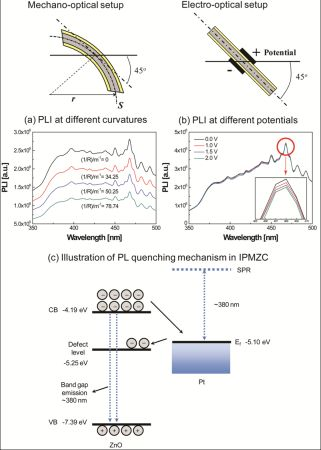
1. Introduction
Materials that can sense changes in their environment (external stimuli) and respond in accordance with these changes are classified as “smart” materials. The type of external stimuli (thermal, magnetic, electrical, chemical, mechanical or radiation) and particular responses to these stimuli (reflectivity change, viscosity change, charge generation or stain) leads to smart materials ranging from ceramics to polymers. Recently, smart materials like electroactive polymers (EAPs) [1–5], piezoelectric ceramics [6–8], shape memory alloys (SMA) [9,10], and carbon ––nanotubes (CNTs) [11,12] have been considered for sensors and actuators development. These materials can be used individually or in combinations with each other for integrated sensor-actuator platform development.
Ionic Polymer Metal Composites (IPMCs) have received great attention due to their electroactive nature. IPMCs undergo bending on application of an electric field in its thickness direction (electromechanical transduction) and generate current on mechanical deformation (mechanoelectric transduction). Typically, an IPMC consists of a thin ionomeric membrane sandwiched between metal electrodes. On hydration, cations along with water molecules move towards the cathode on application of an electric field. The migrated cations induce stress in the polymer due to cation-cation repulsion, causing it to bend. On the other hand, bending an IPMC results in discrete regions of high water density causing water molecules and cations to move from their high-density region to their lower density region. This motion of ions inside the polymer produces a current. IPMCs display several advantages like low actuation voltages (1–3 V), flexibility, chemical stability, large actuation displacements (>1 cm) and long life (∼250,000 cycles). The presence of ionomeric membrane results in large capacitance of IPMCs that can be used for energy storage applications.
Since Oguro et al. [13] observed a Nafion-based IPMC bending actuator; vigorous research on sensor-actuator systems has been carried out using IPMCs in diverse configurations [14–22]. Despite their inherited transduction properties, IPMCs suffer from small force outputs, nonlinear responses and low current generation capabilities. The degree of transduction is dependent on a variety of factors such as the type of polymer used, counter ion in the polymer, the polymer conductivity, the degree of hydration, the electrode quality and the electrode thickness. Wiring an IPMC sensor/actuator has also been observed to be challenging. Besides, existing measurement techniques increase signal losses in mechanoelectric transduction or interfere with actuation. Many applications could be benefited by a measuring technique that could not only enable wireless measurement of IPMC transduction without hampering its electroactive nature. Current state-of-the-art IPMC actuators/sensors do not possess optical properties that can enable noncontact measurement of IPMC output. The commonly used electrodes like platinum and gold being metals have low surface resistance, but need to be wired for any measurement.
In the reported work, a measuring method obtained by depositing ZnO onto IPMCs, creaing what we have termed as an Ionic Polymer Metal-ZnO Composite (IPMZC), potentially imparts electro-mechano-optical characteristics to IPMCs. IPMZC is based on the principle of photoluminescence (PL) quenching. The process of reduction of PL intensity is called quenching. PL quenching has been observed in semiconductor-metal nanostructure systems. Although the mechanism of PL quenching is not very well understood, the reduction in the PL intensity is believed to be dependant on a number of factors like geometry of the metal, particle size and roughness of the metal surface. The resulting quenching could be due to factors like localized excited state dissociation by electric field, exciton-exciton annihilation and interaction of excited states with charge carriers.
ZnO is one of the widely used functional materials due to its unique optical and piezoelectric properties. ZnO has shown to exhibit a wide direct band gap (∼3.37 eV), a good electrical conductivity (∼5 × 10² Ω−1cm−1), and piezoelectric properties [23–25]. The piezoelectric properties of ZnO might be able to convert mechanical energy into electrical energy and such devices could provide potential applications as optical actuators and sensors. ZnO is a good candidate for this application due to its high electrical conductivity and its high PL response in the ultraviolet and visible-wavelength ranges [26–33]. An experimental investigation of the PL (photoluminescence)-quenching [34–40], which is reduction of PL intensity with an increase in applied field or deformation, was performed in the newly developed IPMZC. The attractiveness of this work is the simplicity of the fabrication process and the optical property’s usefulness.
2. Experimental Section
2.1. Fabrication
The polymer electrolyte membrane used for IPMC fabrication was Nafion 117 (Dupont, 0.18 mm thick, 1,100 g/mol of equivalent weight). Platinization on both sides of the Nafion membrane was carried out by the standard electroless deposition techniques [41,42].
ZnO thin films have been deposited by a number of techniques including DC or RF sputtering [43,44], metal organic chemical vapor deposition (MOCVD) [45,46], molecular beam epitaxy (MBE) [47], pulsed-laser deposition [48,49]. Theses techniques all produce high quality ZnO thin films, which are deposited at relatively high substrate temperatures varying from 200 °C to 800 °C. However, these techniques have serious demerits in case of deposition on IPMCs. The process temperatures are too high to deposit the ZnO thin films without damaging the IPMC and it is quite challenging to obtain ZnO films on both sides of the IPMC. The chemical deposition method to produce thin films from aqueous solutions, at low temperature, presents several advantages with respect to other deposition techniques because of large-scale production capability, simplicity and economy [50–52].
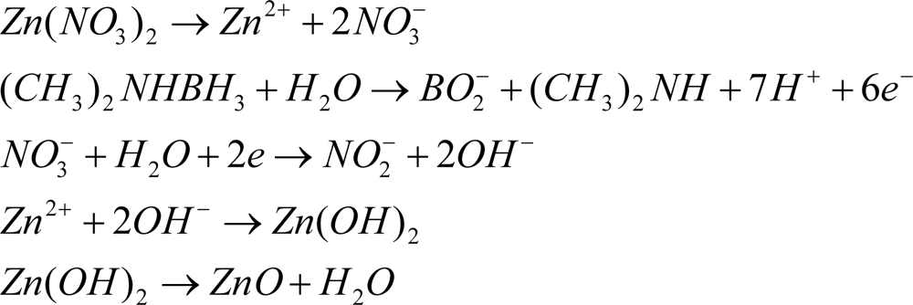
Zinc nitrate, Zn(NO3)2 and reagent grade dimethylaminoborane (DMAB) were purchased from Sigma-Aldrich. ZnO thin films were synthesized on the Pt IPMC in an aqueous solution composed of 0.1 mol/L hydrous zinc nitrate and 0.1 mol/L DMAB maintained at 60 °C. It has been reported that electrical and optical properties of ZnO film depends on the DMAB concentration [53]. ZnO film prepared from the 0.1 mol/L DMAB solution showed best results [54]. An optimum deposition condition for ZnO film (based on temperature and chemical ratio of Zn(NO3)2 and DMAB) as reported in [54] was used. The chemical deposition mechanisms are shown in Scheme 1. The nitrate ion undergoes reduction while DMAB is oxidized.
The chemical deposition method for fabrication of IPMZC produces a uniform coating of ZnO on the IPMC substrate. The chances of thermal stress on the IPMC were minimal as the deposition was performed at temperatures below 100 °C.
2.2. Characterization
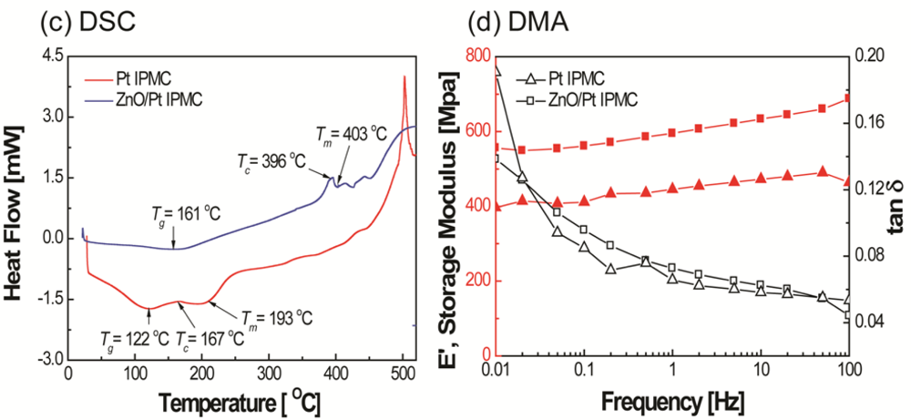
In order to analyze the orientation of ZnO crystals deposited on the electrodes, X-ray diffraction (XRD) patterns of the films were obtained with PANaltical’s X’Pert Pro X-ray diffractometer system with Cu-Kα radiation in the 2θ range (30–70°) with a step size of 0.02°. The shapes and sizes of ZnO grains were observed using a scanning electron microscopy (SEM, Hitachi, S-4700) and the compositions of the IPMZC were characterized in cross-sectional view using energy dispersive x-ray spectroscopy (EDS, Hitachi S-4700 equipped with Oxford EDS), respectively. Differential scanning calorimeter (DSC, Q-10, TA instrument) was performed in nitrogen atmosphere with 10 °C min−1 heating rate.
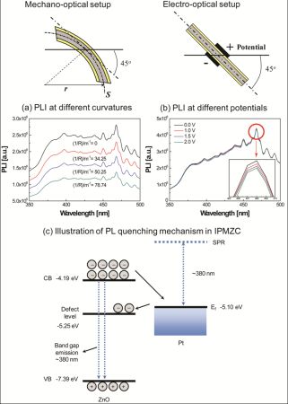
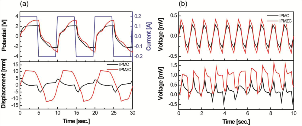
The electromechanical and mechanoelectrical properties of the IPMC were investigated by using the potentiostat/galvanostat and shaker systems. IPMZCs were cut into a size of 1 cm width and 5 cm length. The actuation responses of typical IPMCs and IPMZCs were measured using chrono-potentiometry with a square wave for 5 s as a function of the applied current (−200 to 200 mA). Using a laser displacement sensor, the displacement was measured at a distance of 2 cm from the tip of the sample. The experimental set-up is shown in Figure 1.
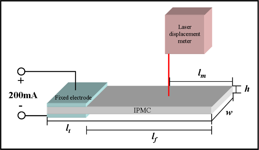
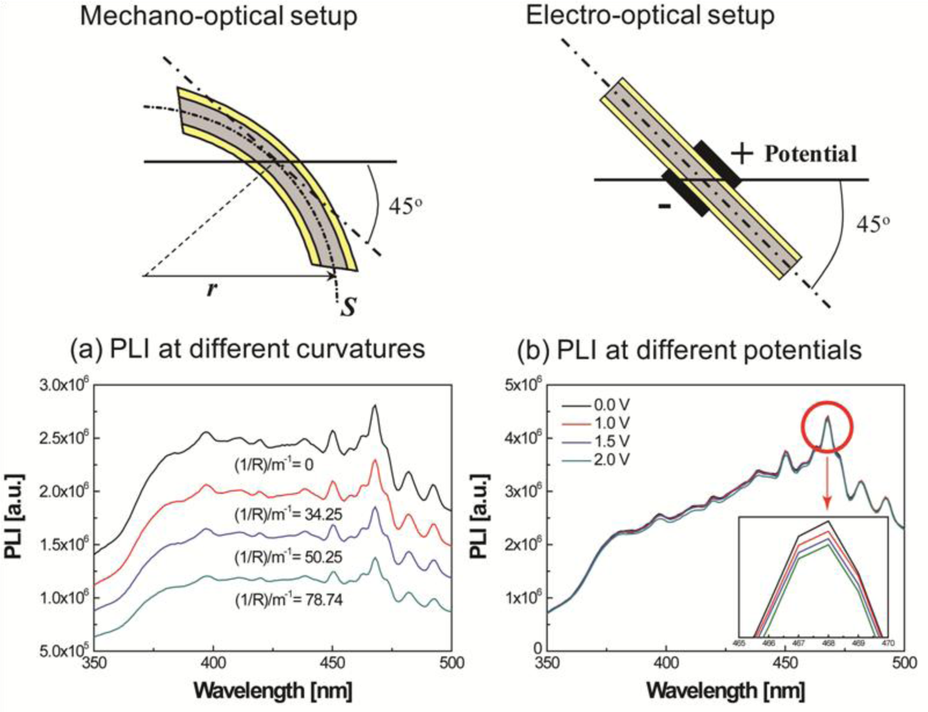
For luminescence investigation, the IPMZC sample was photo-excited at room temperature by an excitation wavelength of 280 nm (xenon arc lamp) in the PL apparatus (FluoroMax-3) and the emission was monitored in the wavelength range 350–500 nm. The opto-electrical property of the IPMZC was characterized with the use of a power supply (potential variation: 0–2.0 V) during the PL measurement as shown in Figure 2. For characterizing opto-mechanical response the IPMZC sample was placed with different curvature while the UV excitation was focused at the center of the sample.
3. Results and Discussion
Depositing ZnO onto an IPMC potentially imparts mechano-electro-optical characteristics to the IPMC by integrating the optical properties of ZnO with the tailored electrical properties of an IPMC. The use of an IPMC as the substrate for the ZnO deposition presents certain advantages: (i) the IPMC, as a soft actuator, displays a high deformation with the application of an electric field; (ii) the porous electrodes of the IPMCs enhance the binding of the ZnO on IPMCs; and (iii) the metallic electrodes (Pt or Au) of the IPMC impart a low resistivity and, at the same time, eliminate the need of additional electrodes in a hybrid system. PL quenching in ZnO-Pt nanoparticles has been previously observed [55].
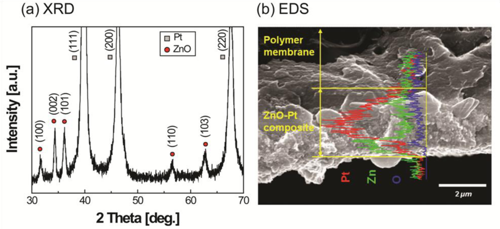
The XRD results in Figure 3(a) show all of the diffraction peaks that were assigned to the ZnO. The ZnO had a wurtzite structure and included a preferred growth orientation along the c-axis, perpendicular to the substrate.
Although other diffraction peaks were observed, the c-axis (002) plane of the ZnO showed higher intensity than other additional peaks. The XRD diffraction patterns of platinum are from the electrode material of the IPMC. The observed reflections at (111), (200), and (220) are clear and support a crystal structure of metal electrode. From the EDS results in Figure 3(b), the concentration of zinc elements is clearly higher than that of oxygen, indicating that the thin ZnO film is zinc-rich. Most undoped ZnO has n-type behavior, which is closely related to an oxygen-deficient non-stoichiometry. The electrical resistivity of the films was strongly affected by the oxygen vacancy and/or zinc interstitials. This mechanism can be easily understood by understanding that the electrical conductivity of the ZnO can be increased proportionally with increasing the oxygen vacancy.
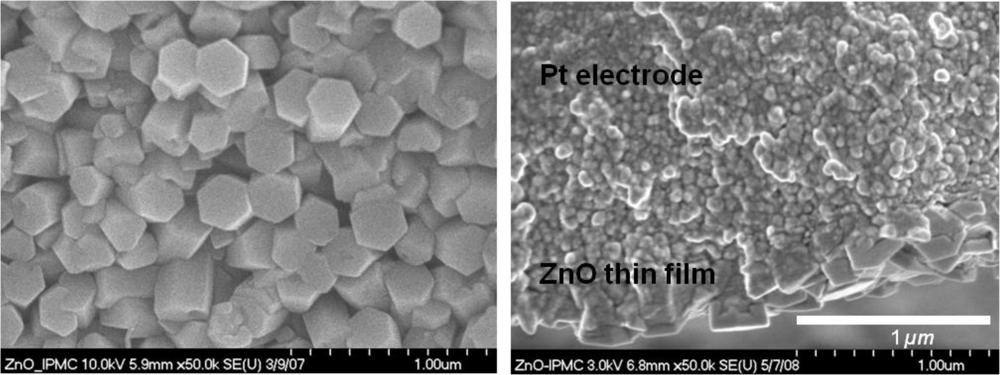
An increase in the melting temperature and storage modulus can be observed from Figure 3(c,d), respectively. This increase is believed to be due to the crystalline layer of ZnO on IPMC. From the SEM image (Figure 4), it was observed that the ZnO crystals grown on an IPMC have a hexagonal shape, and the grains display sizes in the range of 200–300 nm. It can be seen from the cross-sectional view, the thickness of the ZnO thin film ranges between 300–400 nm. However, it should be noted that the ZnO on Pt is susceptible to removal on rubbing or abrasion. Hence care must be taken while working with the IPMZC.
Figure 5 compares the properties of IPMZC with a typical IPMC with a platinum electrode. The output potential results indicate that the IPMZC (−3 to 3 V) responds better electrically with the applied current input (top in Figure 5(a)). According to the corresponding displacement, the IPMZC has a large and stable bending deformation, around 22 mm (peak to peak), which is higher than that of IPMC, shown Figure 5(a).
In addition, the induced displacement of conventional IPMCs shows relaxation behavior, but much less than shown by the IPMZC. This could be due to the combined effect of the piezoelectric property of ZnO and the ionic nature of IPMC, as well as the increase of the conductivity of the “zinc-rich” ZnO thin films. Hence, the displacement on the application of the current becomes more linear. Improvements have been observed in the voltage produced by IPMZC on the application of 12.7 mm sinusoidal displacement, u, with the frequency of 1 Hz, as seen in Figure 5(b). These enhancements can be understood by utilizing the piezoelectric [56] and IPMC mechanoelectric equations below [18]. The output of IPMZC is the resultant of the output from the ZnO layer and the IPMC substrate layer. The voltage, in V, from ZnO layer is calculated as [57]:
The final sensor equation for open circuit voltage is used to calculate the voltage output from the IPMC [18]:
The difference in the simulated and experimental data in Figure 5(b) is due to the fact that Equations (1–3) do not take into account the charge transport inside the IPMC and IPMZC. These equations are rather dependent on the sample dimensions, stiffness and overall impedance. Also the effect of interfacial layer between the ZnO and platinum is neglected. Despite these limitations, these equations can be used to predict the trend in the IPMZC output and its dependence on properties like dimensions, stiffness and impedance.
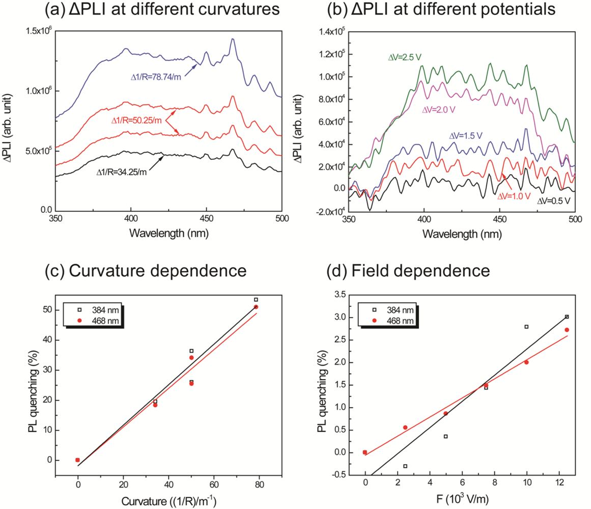
The IPMZC sample was photo-excited by an excitation wavelength of 280 nm (xenon arc lamp) in the PL apparatus. The spectra of the sample display a broad emission band with some vibronic structure. A weak emission peak at the wavelength around 384 nm corresponds to the ultra-violet wave near the band edge emission. A relatively strong emission, around 468 nm, has been observed during this process (Figure 6).
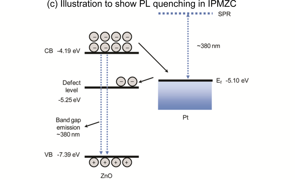
The maximum PL intensity was observed when there was no deformation and no electric field present in the IPMZC. In order to explain the PL quenching in IPMZC a schematic diagram (Figure 6(c)) is plotted. As shown in the figure the conduction band of ZnO is located at −4.19 eV and valence band is −7.39 eV. The Fermi level of platinum is at −5.10 eV. A band-gap emission occurs when an electron in the conduction band combines with the hole in valence band. Quenching occurs since the electron in the conduction band of ZnO goes to the Fermi level of platinum which in turn transfers the electron to the defect band of ZnO. This reduces the the band gap in ZnO resulting in decrese in the PL intensity.
In order to clearly observe the effects of curvature and the applied potential, a differential of the intensity was calculated as follows: the intensities measured at different voltages and curvatures were subtracted from the intensity at the initial condition. The operating range of the new IPMZC as 375 nm to 475 nm wavelengths was the result. The quenching efficiency of the mechano-optical and electro-optical properties, , were calculated, independent of each other, with different curvatures and electric fields applied to the sample and is then defined as:
In order to investigate PL-quenching due to the different curvatures of the IPMZC, the sample was bent, and the corresponding intensity was measured (Figure 7(a)). The differential PL intensity and the quenching increased with the curvature. The quenching could be due to the change in orientation or the localized density of ZnO crystals. Analyzing the graph (Figure 7(c)), the quenching efficiency reached a maximum of 53.4% and 50.9% at 384 nm and 468 nm, respectively, while the bending curvature was set to 78.74/m. The electro-optical properties of the IPMZC were also characterized with a potential variation (0–2.5 V) during the PL measurement (inset in Figure 7(b)). Care was taken to as to avoid any bending of the sample on application of voltage across IPMZC. As the electric field increased, the PL intensity decreased. This decrease in intensity with increasing voltage (hence of electric field), can be due to the increase in the depletion region, or dead layer, because of the spatial separation of electrons and holes. The PL-quenching efficiency was measured to be 3.01% at 384 nm when an electric field (12.5 × 10³ V/m) is applied across the IPMZC. This efficiency is relatively smaller than that obtained through the bending process, shown in Figure 7(d). Due to its linear dependence on an optical property, associated with the mechanical deformation and the electric field, the IPMZC is an attractive contender as a non-contact type actuation sensor.
4. Conclusions
In summary, a novel IPMZC has been successfully fabricated to incorporate the optical and piezoelectric properties of ZnO onto the electroactive nature of an IPMC through chemical deposition technique. The structure of ZnO thin films was observed to be hexagonal in shape, with a grain size of 200–300 nm and average thickness of 300–400 nm. From the EDS result, it was found that the concentration of zinc is higher than that of oxygen, indicating that the ZnO thin film was zinc-rich. The resulting IPMZC exhibits significant transduction property effects. The optical effect of the IPMZC was characterized using photoluminescence. The new IPMC is shown to have working range between 375 to 475 nm wavelengths. The changes in the PL intensity, due to mechanical deformation and an external electric field, can be caused by a variety of reasons: (i) changes in the orientation of the ZnO crystal due to a change in the IPMZC curvature, (ii) changes in the localized density of the ZnO crystal with respect to the imposed strain of the polymer composite, and (iii) variations in the current flow through the high carrier densities in the device.
Further work for the development of an integrated sensor-actuator platform with a ZnO layer for feedback could be performed. In addition, there is need to probe into the effect of grain size and piezoelectric coefficient on the electroactive behavior of IPMZCs.
Supplementary Materials
sensors-11-04674-s001.pdfAcknowledgments
We appreciate the financial support from the U.S. National Science Foundation (#0713075).
References
- Shahinpoor, M; Kim, K. Ionic polymer-metal composites: I. Fundamentals. Smart Mater. Struct 2001, 10, 819–833. [Google Scholar]
- Shahinpoor, M; Bar-Cohen, Y; Simpson, JO; Smith, J. Ionic polymer-metal composites (IPMCs) as biomimetic sensors, actuators and artificial muscles—a review. Smart Mater. Struct 1998, 7, R15–R30. [Google Scholar]
- Nemat-Nasser, S; Wu, Y. Tailoring the actuation of ionic polymer-metal composites. Smart Mater. Struct 2006, 15, 909–923. [Google Scholar]
- Nemat-Nasser, S; Li, JY. Electromechanical response of ionic polymer-metal composites. J. Appl. Phys 2000, 87, 3321–3331. [Google Scholar]
- Park, I-S; Jung, K; Kim, D; Kim, S-M; Kim, KJ. Physical principles of ionic polymer-metal composites as electroactive actuators and sensors. MRS Bull 2008, 33, 190–195. [Google Scholar]
- Dong, W; Lu, X; Cui, Y; Wang, J; Liu, M. Fabrication and characterization of microcantilever integrated with PZT thin film sensor and actuator. Thin Solid Films 2007, 515, 8544–8548. [Google Scholar]
- Kawai, H. The piezoelectrictity of polyvinylidene fluoride. Jpn. J. Appl. Phys 1969, 8, 975–976. [Google Scholar]
- Suski, J; Largeau, D; Steyer, A; van de Pol, FCM; Blom, FR. Optically activated ZnO/SiO2/Si cantilever beams. Sens. Actuat A 1990, 24, 221–225. [Google Scholar]
- Kim, B; Lee, MG; Lee, YP; Kim, YI; Lee, GH. An earthworm-like micro robot using shape memory alloy actuator. Sens. Actuat. A 2006, 125, 429–437. [Google Scholar]
- Chiodo, JD; Jones, N; Billett, EH; Harrison, DJ. Shape memory alloy actuators for active disassembly using ‘smart’ materials of consumer electronic products. Mater. Des 2002, 23, 471–478. [Google Scholar]
- Iijima, S. Helical microtubules of graphitic carbon. Nature 1991, 354, 56–58. [Google Scholar]
- LeRoy, BJ; Lemay, SG; Kong, J; Dekker, C. Electrical generation and absorption of phonons in carbon nanotubes. Nature 2004, 432, 371–374. [Google Scholar]
- Oguro, K; Kawami, Y; Takenaka, H. Bending of an ion-conducting polymer film-electrode composite by an electric stimulus at low voltage. J. Micromachine Soc 1992, 5, 27–30. [Google Scholar]
- Bonomo, C; Fortuna, L; Giannone, P; Graziani, S. A sensor-actuator integrated system based on IPMC. Proc. IEEE Sens 2004, 1, 489–492. [Google Scholar]
- Ko, BG; Kwon, HC; Lee, SJ. A self-sensing method for IPMC actuator. Adv. Sci. Tech 2008, 56, 111–115. [Google Scholar]
- Chen, Z; Kwon, K; Tan, X. Integrated IPMC/ PVDF sensory actuator and its validation in feedback control. Sens. Actuat. A 2007, 144, 231–241. [Google Scholar]
- Hunt, A; Chen, Z; Tan, X; Kruusmaa, M. Feedback control of a coupled IPMC (Ionic polumer metal composite) sensor-actuator. Proceedings of ASME Dynamics Systems and Control Conference (DSCC2009), Hollywood, CA, USA, 12–14 October 2009; pp. 485–491.
- Tiwari, R; Kim, KJ; Kim, S. Ionic Polymer-Metal Composite as energy harvesters. Smart Struct. Syst 2008, 4, 549–563. [Google Scholar]
- Park, I-S; Tiwari, R; Kim, KJ. Sprayed sensor using IPMC paint. Adv. Sci. Tech 2008, 61, 59–64. [Google Scholar]
- Tiwari, R; Kim, KJ. Disc-shaped IPMCs for use in Mechano-electrical applications. Smart Mater. Struct 2010, 19, 065016. [Google Scholar]
- Tiwari, R; Kim, KJ. Effect of metal diffusion on mechanoelectric property of Ionic Polymer-Metal Composite. Appl. Phys. Lett 2010, 97, 244104. [Google Scholar]
- Sadeghipour, K; Salomon, R; Neogi, S. Development of a novel electrochemically active membrane and smart material based vibration sensor/damper. Smart Mater. Struct 1992, 1, 172–179. [Google Scholar]
- Jelison, GE, Jr; Boatner, LA. Optical functions of uniaxial ZnO determined by generalized ellipsometry. Phys. Rev. B 1998, 58, 3586–3589. [Google Scholar]
- Webb, JB; Williams, DF; Buchanan, M. Transparent and highly conductive films of ZnO prepared by RF reactive magnetron sputtering. Appl. Phys. Lett 1981, 39, 640–642. [Google Scholar]
- Verghese, PM; Clarke, DR. Piezoelectric contributions to the electrical behavior of ZnO varistors. J. Appl. Phys 2000, 87, 4430–4438. [Google Scholar]
- Xue, H; Xu, X-L; Chen, Y; Zhang, G-H; Ma, S-Y. Optical properties of nano-ZnO embedded SiO2 films. J. Funct. Mater 2009, 40, 700–703. [Google Scholar]
- Nagata, T; Shimura, T; Ashida, A; Fujimura, N; Ito, T. Electro-optical property of ZnO:X (X = Li, Mg) thin films. J Cryst Growth 2002, 237–239, 533–537. [Google Scholar]
- Chen, K; Wu, W; Zheng, S. Study on ammonia-sensitive optical property of ZnO/TiO2 multi-layer thin film. Laser Technol 2001, 25, 209–213. [Google Scholar]
- Sun, J; Liang, H; Zhao, J; Feng, Q; Bian, J; Zhao, Z; Zhang, H; Luo, Y; Hu, L; Du, G. Annealing effects on electrical and optical properties of ZnO films deposited on GaAs by metal organic chemical vapor depositon. Appl. Surf. Sci 2008, 254, 7482–7485. [Google Scholar]
- Han, X; Wang, G; Jie, J; Wang, Q; Li, D. Optical properties of ZnO cone arrays and influence of annealing on optical properties of ZnO-Zn coaxial nanocables. Proc. SPIE 2006, 6349, 154. [Google Scholar]
- Chen, KJ; Hung, FY; Chang, SJ; Hu, ZS. Microstructures, optical and electrical properties of In-doped ZnO thin films prepared by sol-gel method. Appl. Surf. Sci 2009, 255, 6308–6312. [Google Scholar]
- Wei, XQ; Zhang, Z; Yu, YX; Man, BY. Comparative study on structural and optical properties of ZnO think films prepared by PLD using ZnO powder target and ceramic target. Opt. Laser Technol 2009, 41, 530–534. [Google Scholar]
- Sofiani, Z; Derkowska, B; Dalasinski, P; Lukasiak, Z; Baa, W; Addou, M; Mehdi, AL; Dghughi, L; Sahraoui, B. Nonlinear optical effects of thin layers based on ZnO:Ce nanostructures. Proceedings of the 7th International Conference on Transparent Optical Networks (ICTON), Barcelona, Spain, 4–7 July 2005; p. 372.
- Huang, H; Dorn, A; Nair, GP; Bulovi, V; Bawendi, MG. Bias induced photoluminescence quenching of single colloidal quantum dots embedded in organic semiconductors. Nano Lett 2007, 7, 3781–3786. [Google Scholar]
- Kalinowskia, J; Stampor, W; Cocchi, M; Virgili, D; Fattori, V. Electric-field-induced quenching of photoluminescence in photoconductive organic thin film structures based on Eu3+ complexes. J. Appl. Phys 2006, 100, 034318. [Google Scholar]
- Naumov, AV; Bachilo, SM; Tsyboulski, DA; Weisman, RB. Electric-field quenching of carbon nanotubes photoluminescence. Nano Lett 2008, 8, 1527–1531. [Google Scholar]
- Deussen, M; Bolivar, PH; Wegmann, G; Kurz, H; Bassler, HB. Chem. Phys 1996, 207, 147–157.
- Achtstein, AW; Karl, H; Stritzker, B. Field induced photoluminescence quenching and enhancement of CdSe nanocrystals embedded in SiO2. Appl. Phys. Lett 2006, 89, 061103. [Google Scholar]
- Muschik, T; Schwas, R; Curtins, H; Fwre, M. Photoluminescence quenching by electric fields in hydrogenated amorphous silicon. IEEE Photovoltaic Spec. Confer 1988, 1, 191–195. [Google Scholar]
- Scheblykin, I; Zoriniants, G; Hofkens, J; Feyter, SD; Auweraer, MVD; Schryver, FCD. Photoluminescence intensity fluctuations and electric field induced photoluminescence quenching in individual nanoclusters of poly(phenylenevinylene). Chem. Phys. Chem 2003, 4, 260–267. [Google Scholar]
- Kim, KJ; Shahinpoor, M. Ionic polymer-metal composites: II. Manufacturing techniques. Smart Mater. Struct 2003, 12, 65–79. [Google Scholar]
- Oguro, K. Recipe-IPMC, Bar-Cohen, Y, Ed.; Available online: http://ndeaa.jpl.nasa.gov/nasa-nde/lommas/eap/IPMC_PrepProcedure.htm (accessed on 1 February 2011).
- Hickernell, FS. DC triode sputtered zinc oxide surface elastic wave transducers. J. Appl. Phys 1973, 44, 1061–1071. [Google Scholar]
- Itoh, T; Suga, T. Force sensing micro-cantilever using sputtered zinc oxide thin film. App. Phys. Lett 1994, 64, 37–39. [Google Scholar]
- Smith, FTJ. Metalorganic chemical vapor deposition of oriented ZnO films over large areas. Appl. Phys. Lett 1983, 43, 1108–1111. [Google Scholar]
- Lau, CK; Tiku, SK; Lakin, KM. Growth of epitaxial ZnO thin films by organometallic chemical vapor deposition. J. Electrochem. Soc 1980, 127, 1843–1847. [Google Scholar]
- Tang, ZK; Wong, GKL; Yu, P; Kawasaki, M; Ohtomo, A; Koinuma, H; Segawa, Y. Room-temperature ultraviolet laser emission from self-assembled ZnO microcrystallite thin films. Appl. Phys. Lett 1998, 72, 3270–3272. [Google Scholar]
- Joseph, M; Tabata, H; Kawai, T. Ferroelectric behavior of Li-doped ZnO thin films on Si(100) by pulsed laser deposition. Appl. Phys. Lett 1999, 74, 2534–2536. [Google Scholar]
- Son, CS; Kim, SM; Kim, YH; Kim, SI; Kim, YT; Yoon, KH; Choi, IH; Lopez, HC. Deposition-temperature dependence of ZnO/Si grown by pulsed laser deposition. J. Kor. Phys. Soc 2004, 45, S685. [Google Scholar]
- Ristov, M; Sinadinovski, GJ; Grozdanov, I; Mitreski, M. Chemical deposition of ZnO films. Thin Solid Films 1987, 149, 65–71. [Google Scholar]
- Mizuta, T; Ishibashi, T; Minemoto, T; Takakura, H; Hamakawa, Y. Chemical deposition of zinc oxide thin films on silicon substrate. Thin Solid Films 2006, 515, 2458–2463. [Google Scholar]
- Kim, S-M; Tiwari, R; Kim, KJ. A novel ionic polymer-metal composite incorporating Zno thin film. Proceedings of the SPIE Smart Material and Structures Conference, San Diego, CA, USA, March 2009.
- Izaki, M; Omi, T. Transparent zinc oxide films chemically prepared from aqueous solution. J. Electrochem. Soc 1997, 144, L3–L5. [Google Scholar]
- Izaki, M; Katayama, J. Characterization of boron-incorporated zinc oxide film chemically prepared from an aqueous solution. J. Electrochem. Soc 2000, 147, 210–213. [Google Scholar]
- Lin, JM; Lin, HY; Cheng, CL; Chen, YF. Giant enhancement of bandgap emission of ZnO nanorods by platinum nanoparticles. Nanotechnology 2006, 17, 4391–4394. [Google Scholar]
- Heywang, W; Lubitz, K; Wersing, W. Piezoelectricity: Evolution and Future of a Technology, 1st ed; Springer: Berlin, Germany, 2008. [Google Scholar]
- Motamedi, ME; Andrews, AP; Brower, E. Accelerometer sensor using piezoelectric ZnO thin films. Proceedings of IEEE Ultrasonics Symposium, San Diego, CA, USA, 27–29 October 1982; pp. 303–307.
- Gopal, P; Spaldin, NA. Polarization, piezoelectric constants, and elastic constants of ZnO, MgO, and CdO. J. Electron. Mater 2006, 35, 538–542. [Google Scholar]


© 2011 by the authors; licensee MDPI, Basel, Switzerland. This article is an open access article distributed under the terms and conditions of the Creative Commons Attribution license (http://creativecommons.org/licenses/by/3.0/).
Share and Cite
Kim, S.-M.; Tiwari, R.; Kim, K.J. A Novel Ionic Polymer Metal ZnO Composite (IPMZC). Sensors 2011, 11, 4674-4687. https://doi.org/10.3390/s110504674
Kim S-M, Tiwari R, Kim KJ. A Novel Ionic Polymer Metal ZnO Composite (IPMZC). Sensors. 2011; 11(5):4674-4687. https://doi.org/10.3390/s110504674
Chicago/Turabian StyleKim, Sang-Mun, Rashi Tiwari, and Kwang J. Kim. 2011. "A Novel Ionic Polymer Metal ZnO Composite (IPMZC)" Sensors 11, no. 5: 4674-4687. https://doi.org/10.3390/s110504674