Quantitative Cross-Platform Performance Comparison between Different Detection Mechanisms in Surface Plasmon Sensors for Voltage Sensing


College of Biomedical Engineering, Rangsit University, Pathum Thani 12000, Thailand
*
Author to whom correspondence should be addressed.
†
These authors contributed equally to this work.
Sensors 2018, 18(9), 3136; https://doi.org/10.3390/s18093136
Submission received: 4 September 2018
/
Revised: 11 September 2018
/
Accepted: 13 September 2018
/
Published: 17 September 2018
(This article belongs to the Special Issue Surface Plasmon Resonance Sensing 2019)
Abstract
:Surface plasmon Resonance (SPR) has recently been of interest for label-free voltage sensing. Several SPR structures have been proposed. However, making a quantitative cross-platform comparison for these structures is not straightforward due to (1) different SPR measurement mechanisms; (2) different electrolytic solution and concentration in the measurement; and (3) different levels of external applied potential. Here, we propose a quantitative approach to make a direct quantitative comparison across different SPR structures, different electrolytic solutions and different SPR measurement mechanisms. There are two structures employed as example in this theoretical study including uniform plasmonic gold sensor and bimetallic layered structure consisting of uniform silver layer (Ag) coated by uniform gold layer (Ag). The cross-platform comparison was carried by several performance parameters including sensitivity (S), full width half maximum (FWHM) and figure of merit (FoM). We also discuss how the SPR measurement mechanisms enhance the performance parameters and how the bimetallic layer can be employed to enhance the FoM by a factor of 1.34 to 25 depending on the SPR detection mechanism.
1. Introduction
Voltage sensing has been a crucial tool used to study important biological processes, such as, neurotransmitter signaling [1,2,3], cell membrane voltage sensing [4] and electrical signals in cardiac cells [5], muscles [6] and skin tissues [7]. Scientists and engineers have employed and developed several optical-based techniques to measure electrophysiological potentials in cells and cell membranes including the use of fluorescence dyes [8,9] and interferometric detection through microfiber [10,11]. However, there are some issues that still need to be addressed. Although the fluorescence dyes can be combined with microscopy techniques allowing sub-cellular activities to be imaged, they however might affect the nature of the biological samples and obscure the accuracy of the voltage measurement [12]. The fluorescence labelling also suffers from photobleaching, making a long run experiment not practical [13]. The microfiber approach requires the microfiber to be placed very close to the sample, making the optical alignment difficult and the microfiber also obscures the sample accessibility [14].
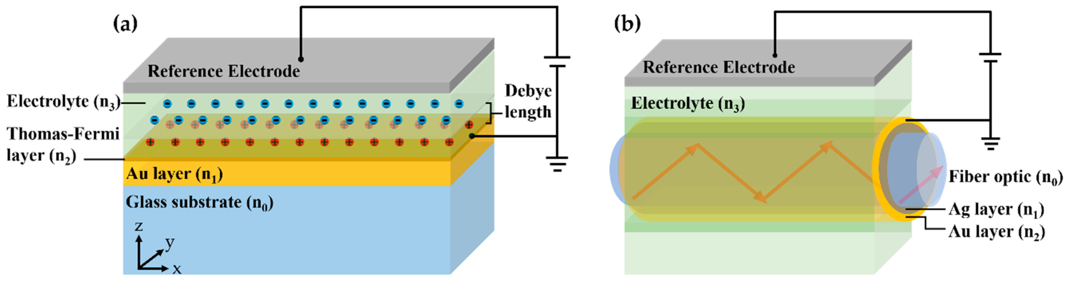
Recently, there has been an interest in employing label-free detection using surface plasmon resonance (SPR) as a voltage sensing platform for biological samples [15,16,17,18,19]. The SPR has been a gold standard for real-time binding kinetics studies [20] and very low concentration biological measurements [21]. The theory and applications for SPR in biosensing have been very well established. However, the application of SPR in voltage sensing has not been reported much in the literature. Abayzeed et al. [17] proposed a model based on the Drude model [22] to calculate the effect of charge potential on the electron density and refractive index in Thomas-Fermi length of uniform plasmonic gold layer as shown in Figure 1a. They have also experimentally validated and found that their experimental results agree very well with the model. Huang et al. [18] proposed a bimetallic layer consisting of a silver layer coated by a gold layer wrapping around a fiber optic core as shown in Figure 1b. Zhang et al. [23] proposed a periodic array of plasmonic nanorods reporting an ultra-sensitive voltage detection. However, there is no obvious way to make a direct performance comparison between these structures, since the structures used (1) different types of electrolytes and concentrations, as well as (2) different optical detection mechanisms and incident wavelengths.
In this paper, we develop and propose a theoretical framework to evaluate and compare the performance of a uniform plasmonic gold sensor and bimetallic layer for voltage sensing using Fresnel equations. These two structures were employed as an example for the proposed procedure. It is noted that the proposed concept can also be applied to some other SPR structures and biosensing in general. To the best of the authors’ knowledge, this has never been reported in the literature before. We also discuss a feasible bimetallic structure, which enhanced the sensitivity and the FoM by a factor of 1.34 to 25 as discussed in detail in the later section.
2. Materials and Methods
2.1. Effect of External Applied Voltage on the Refractive Index of Plasmonic Metal
2.1.1. Gouy-Chapman-Stern Model
In this paper, we follow a model developed by Abayzeed et al. [17]. The optical properties of the metal are modelled by a double layer capacitor. When external voltage is applied to the SPR metal sensor, there are charges confined at the interface between the electrolyte and the metal surface as shown Figure 1a. These charges are confined in Debye length, which is defined as the distance from the sensor surface that the applied potential is dropped to 1/e level [24] as shown in Figure 2. The interfacial potential can be calculated for different electrolytes and voltage potentials using Gouy-Chapman-Stern model [24]. The model considers the applied voltage potential, electrolyte concentration, number of valence ions, ion density and optical permittivity of the electrolyte. The voltage potential is a function of distance from the metal surface z and is given by:
where
- is the voltage potential as a function of distance from the metal surface, in volt (V).
- is the applied voltage on the metal surface, in volt (V).
- is the distance from the metal surface towards the electrolyte, in meter (m).
- is the Boltzmann constant, = 1.3806 × 10⁻²³ m2kg s−2K−1.
- is the temperature of the electrolyte in K.
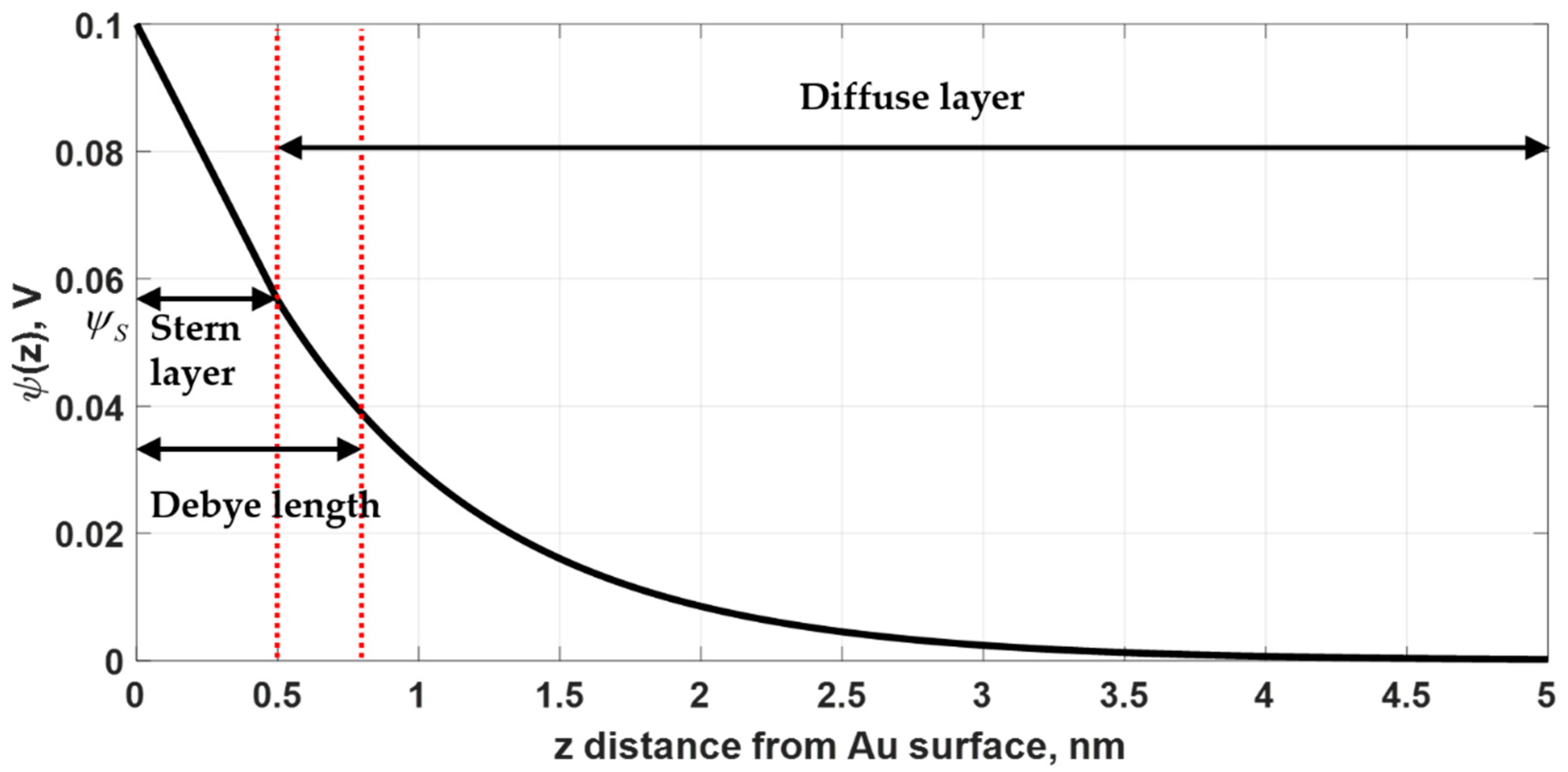
In this paper, the temperature has been fixed to 25 °C or 298.15 K. The term is the thermal energy 4.1162 × 10²¹ J. is the ion density, which can be calculated by concentration in molar in mol/dm3 of the electrolyte solution times Avogadro’s number of 6.0221 × 10²³ and 1000 dm3 conversion factor to the SI unit or is the valence of the ion. In this paper, all the cases were simulated with 0.15 M NaCl electrolyte solution. This molar concentration is equivalent to 0.9% concentration of NaCl solution. The valence of the ion for NaCl is 1 [1]. is the free space permittivity 8.8542 × 10⁻¹² F/m and is the static relative permittivity of the solute, which is water in this case. The for water is 78.54 at 25 °C [2]. is the electron elementary charge of 1.6022 × 10⁻¹⁹ C. is Stern potential, which can be calculated as the potential level from Equation (1) at the solvent molecule size, . The for NaCl molecule is 564.02 pm or 0.5640 nm [3]. By substituting these parameters into Equation (1) and solving the equation, the corresponding Stern potential is 0.0564 V for of 0.1 V as shown in Figure 2.
2.1.2. Capacitor Model
The applied voltage also affects the free electron density in the metal as depicted in Figure 1a. There is an accumulation or depletion of free electrons in the metal in Thomas-Fermi screening length, dTF. Gold has been chosen as the plasmonic material in this study, since gold is chemically stable and is not toxic to the biological samples [25,26,27]. The dTF for gold is 0.5 Å [28]. These two layers, namely Debye layer and Thomas-Fermi layer can then form a double layer capacitor, whose capacitance can be calculated as [23]:
where is the capacitance in F of the double layer capacitor. The rest of the variables are the same as described in Equation (1). The capacitance for the applied voltage of 0.1 V and the 0.15 M NaCl electrolytic solution is 0.7158 F calculated from Equation (2).
2.1.3. Change in Charge Density Due to the Applied Voltage
Once the capacitance is determined, we can then determine the change in free electron density of the plasmonic metal, using the McIntyre model [4], which is given by:
where is the change in free electron density in the plasmonic metal. The plasma frequency can be then determined from the plasma frequency equation given by:
where is the plasma frequency in rad/s. N is the electron density, which is 5.90 × 1028 electrons/m3 [5]. me is the electron mass, which is 9.1094 × 10⁻³¹ kg.
2.1.4. Drude Model
The complex permittivity in the Thomas-Fermi screening length can be calculated from the Drude model [6], which is expressed as:
where
The refractive index of the Thomas-Fermi screening length can be calculated by taking the square root of Equation (5).
This external applied voltage moderates the Thomas-Fermi layer as explained in the models and the gold layer refractive index in the dTF is then modulated by the applied voltage. This consequently reflects in plasmonic shift as shown in the next section.
2.2. Simulation Models
2.2.1. Simulation Model for Uniform Gold Sample
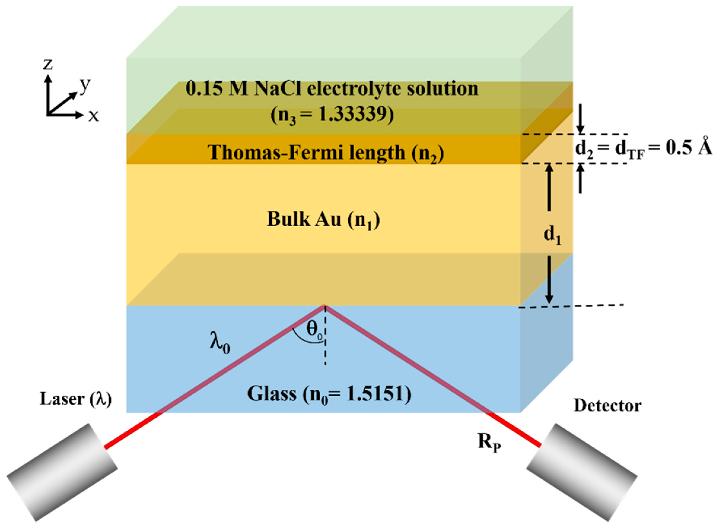
The plasmonic gold layer in this study is modelled by two gold layers as shown in Figure 3. The first layer of gold is the bulk gold layer with thickness d1 and refractive index n1. The refractive indices of the bulk gold layer for each wavelength is extracted from Johnson and Christy 1972 [7]. The second gold layer is the Thomas-Fermi layer with the refractive index n2 and thickness d2 of 0.5 Å. The refractive index of the Thomas-Fermi layer is determined as described in Equation (5) in the earlier section. The p-polarized incident beam with the free-space incident wavelength of and incident angle of is incident on this plasmonic sensor through a glass substrate with refractive index n0 of 1.5151 (BK7) [8]. Reflectance of the p-polarized light Rp is then calculated using Fresnel equations through the transfer matrix approach [9].
2.2.2. Simulation Model for Bimetallic Sample
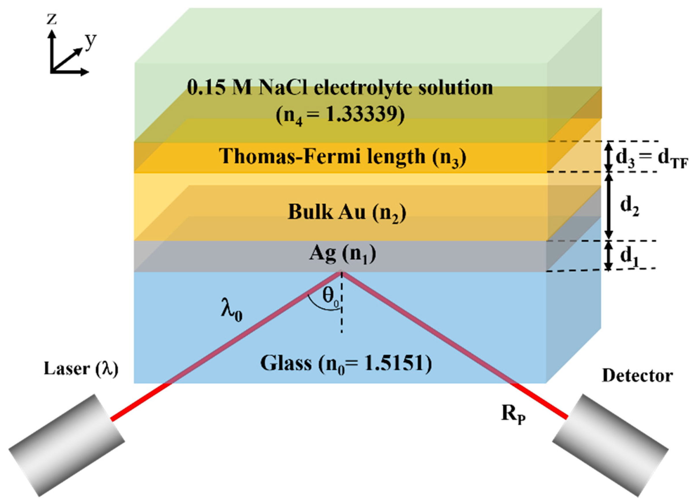
Bimetallic plasmonic sensor for voltage sensing consisting of a uniform silver layer coated by another uniform gold layer as shown in Figure 4 were employed in this study. The simulation concept explained in the above section is also applied for this case. There is a silver layer with a thickness of d1 and a refractive index n1 extracted from Johnson and Christy 1972 [7] coated on the top of the BK7 glass substrate. The silver layer is then coated by a uniform gold layer. In the simulation, the gold layer is simulated using two sublayers, which is firstly the bulk gold layer with a thickness of d2 and the refractive index of n2 extracted from Johnson and Christy 1972 [7], and the Thomas-Fermi length layer with the thickness of d3 of 0.5 Å and refractive index calculated by the models explained in Section 1.
2.2.3. Voltage Range in this Study
It is important to point out that this model is only valid for the applied potential range between −200 mV to 200 mV. The external potential outside this range could lead to a chemical reaction on the surface of the gold and the shape of the SPR dip can be dramatically distorted as reported by Garland et al. [10]. The voltage range in this study was −200 mV to 200 mV, which was in the typical range of typical electrochemical processes in biological samples [11].
2.2.4. Performance Comparison
In SPR measurement, there are several approaches to measure the change in SPR signal including intensity measurement [12] and phase measurement [13]. In this paper, we chose three common practice approaches for SPR measurement which were:
Mechanism 1 (M1) measures the change in plasmonic coupling angle at a fixed incident wavelength as shown in Figure 5a.
Mechanism 2 (M2) measures the change in plasmonic coupling wavelength at a fixed incident angle as shown in Figure 5b.
Mechanism 3 (M3) measures the change in reflectance intensity at a fixed incident angle a fixed incident wavelength as shown in Figure 5c.
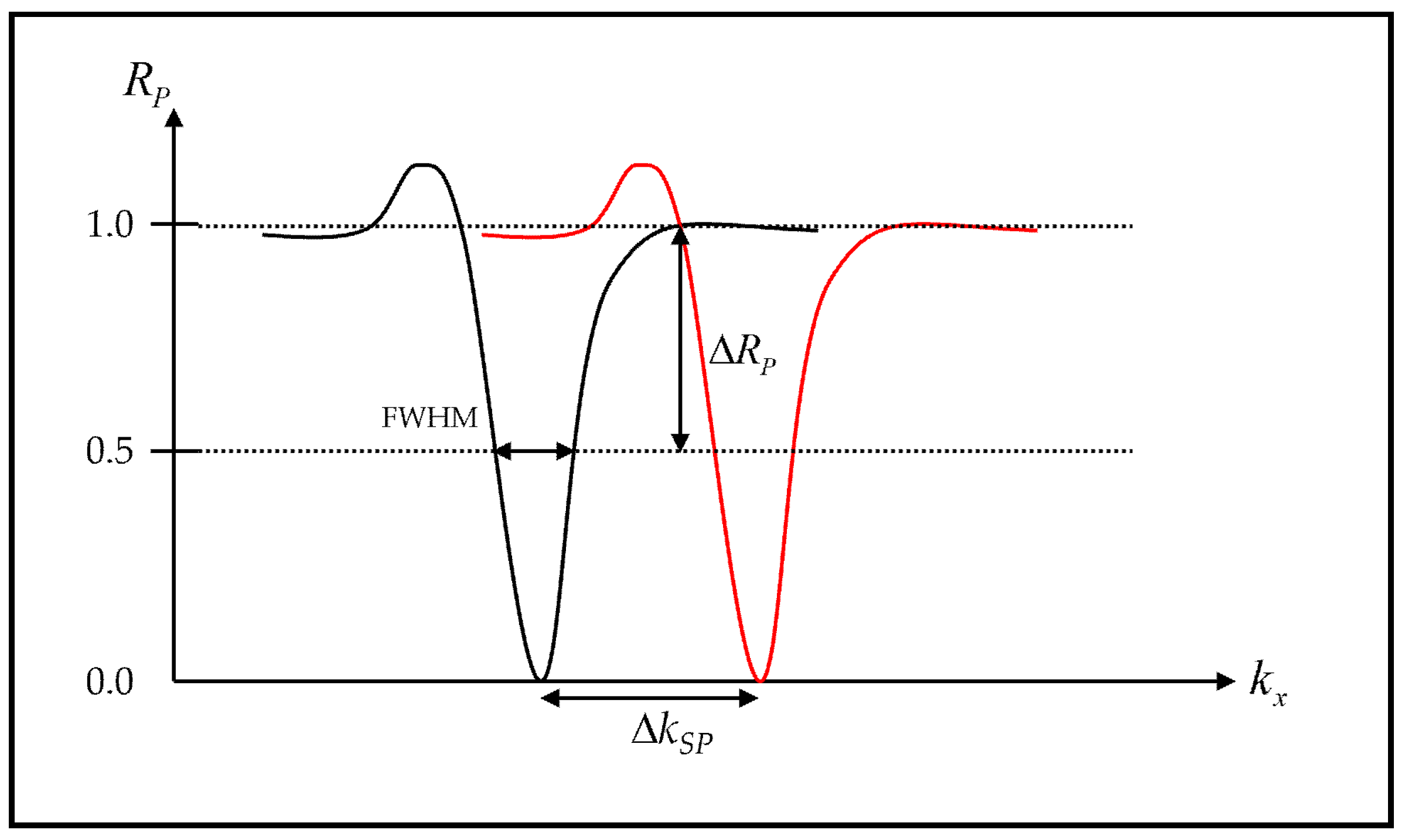
In this paper, we would like to quantify and compare different structures and different detection mechanisms. Let us define some terms to quantify the performance as shown in Figure 6.
2.2.5. Figure of Merit for M1 and M2
The Figure of Merit (FoM) is the term indicating the performance of a sensor. The FoM is defined here as a ratio between sensitivity and the full width half maximum. The FoM term takes into account (1) how much the SPR dip moves and (2) how narrow the SPR dip is. This has been widely accepted as a standard performance parameter for biosensors [14].
The wave vector of the incident light along x-axis, kinc,x is defined as and the wave vector of the surface plasmons is defined as . The sensitivity (S) for M1 and M2 is defined as:
where
- S is the sensitivity term in m−1V−1.
- is the change in plasmonic wave vector.
- is the change in applied potential.
The FWHM is defined as the width in wave vector space that the reflectance intensity is less than 0.5.
2.2.6. Figure of Merit for M3
The FoM for the M3 case is defined as:
where is the sensitivity of the third detection mechanism, which is defined as . The term is the change in reflectance intensity, the term is the reflectance intensity level when of 0 V is applied, and is the normalization factor allowing this M3 FoM to be compared with M1 and M2 FoMs. The value of is 1.5741 × 10⁻⁶. The derivation of the normalization factor will be explained in the next section.
3. Results and Discussion
3.1. Uniform Gold Sample for Voltage Sensing
3.1.1. Measurement Mechanism 1 (M1)
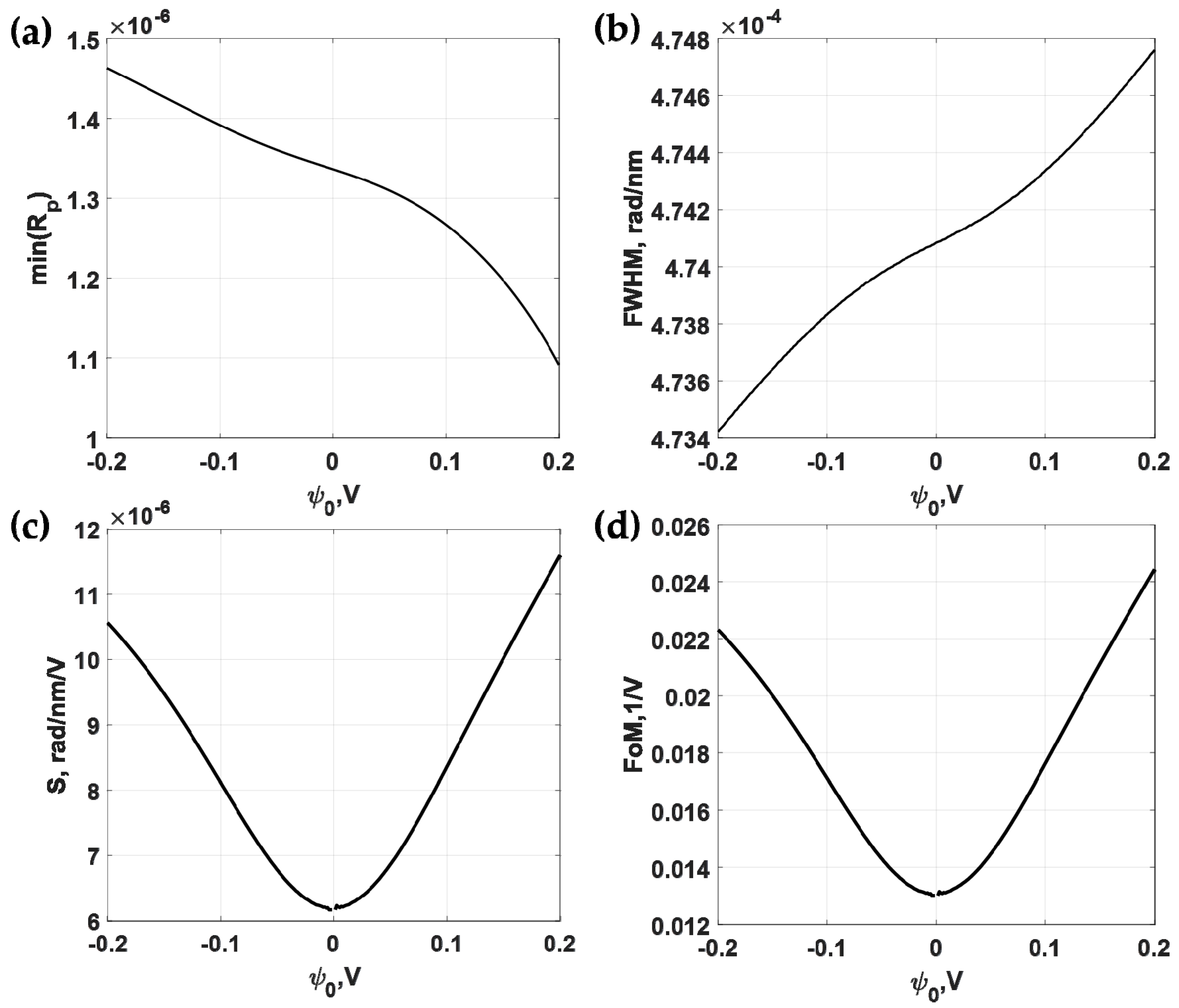
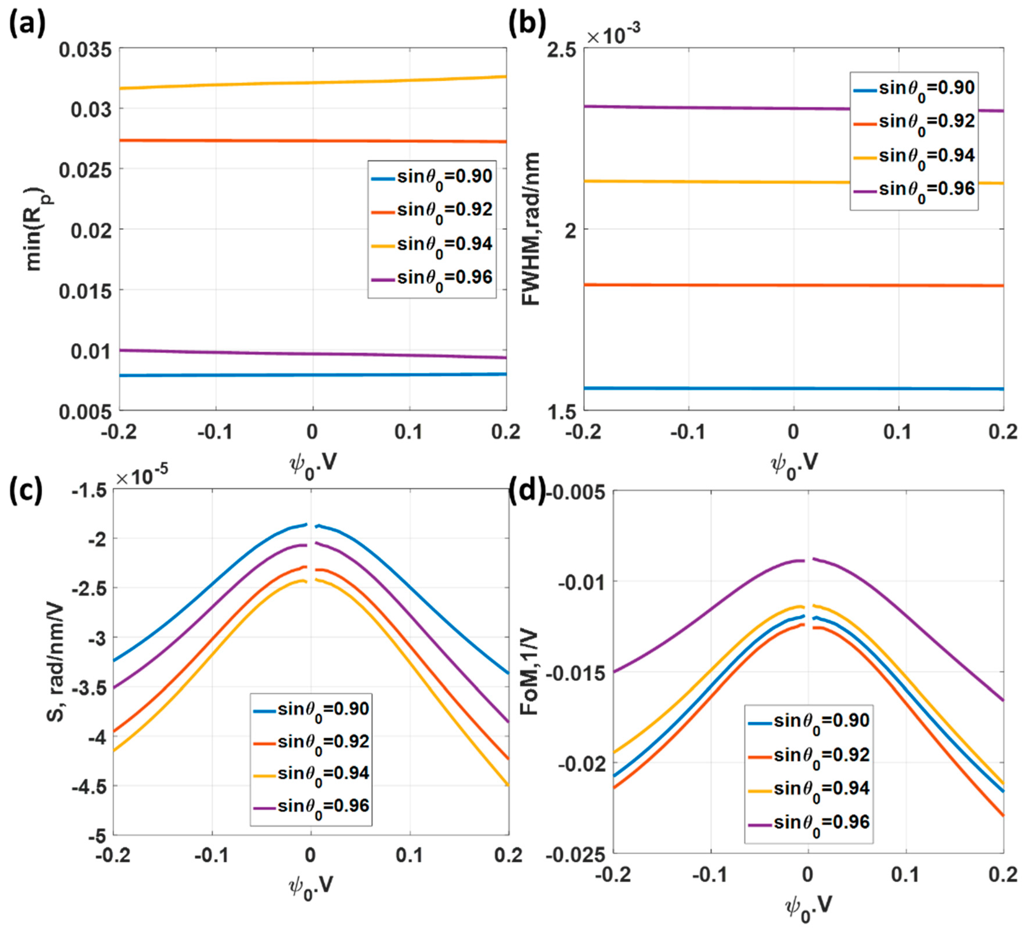
Firstly, let us consider the uniform gold sensor as shown in Figure 3 as a basis to compare the other types of structures. Figure 7a shows reflectance responses of the p-polarized incident light at 632.8 nm (HeNe laser wavelength) incident wavelength when the total gold thickness was varied from 20 nm to 80 nm and the applied potential was of 0 V. The total gold thickness that gave the minimum reflectance dip was 47 nm, which was in the range of optimum gold thickness for SPR sensor [15]. This 47 nm gold sensor was then calculated for different applied voltage levels as shown in Figure 7b. The responses here agree very well with the results reported in Abayzeed et al. [16]. The results in Figure 7b allows us to calculate the defined performance parameters as shown in Figure 8. Figure 8a shows the minimum reflectance intensity level. It can be seen from the figure that the depth of the dip was not affected much by the range of applied voltage level maintaining a decent SPR reflectance dip response over the whole applied voltage range. The FWHM was also not affected much by the applied voltage level as shown in Figure 8b. The variation in the FWHM was within 0.15%. The sensitivity (S) was slightly different for positive and negative potentials and the maximum sensitivity was 1.16 × 10⁻⁵ rad/nm/V at of 0.2 V as shown in Figure 8c. The maximum FoM of 0.0244 V−1 at applied potential of 0.2 V ss shown in Figure 8d.
Another approach to compare this sensitivity is to compare it with bulk refractive index sensitivity as if this 47 nm was employed as a conventional SPR sensor to measure the change in the refractive index of the sample [14]. In other words, n1 and n2 were identical and the refractive index of n3 were varied until the change in or of 1.16 × 10⁻⁵ rad/nm was reached. The change in n3 refractive index required to change the ksp by 1.16 × 10⁻⁵ rad/nm was 2 × 10⁻⁴ RIU. This number does give us some idea of the voltage detection limit of the uniform gold sensor. The current state of the art angular-based SPR platform relying on phase detection can achieve around 10−6 to 10−7 RIU detection limit [17]. The intensity detection mechanism, of course, has a lower RIU detection limit around 10−5 to 10−6 RIU [12]. This indicates the voltage detection limit of the uniform gold sensor is around 50 mV for 10−5 RIU detection limit, which is not very good. Therefore, another type of SPR sensor and detection mechanism was also developed and reported by several authors [18,19].
3.1.2. Measurement Mechanism 2 (M2)
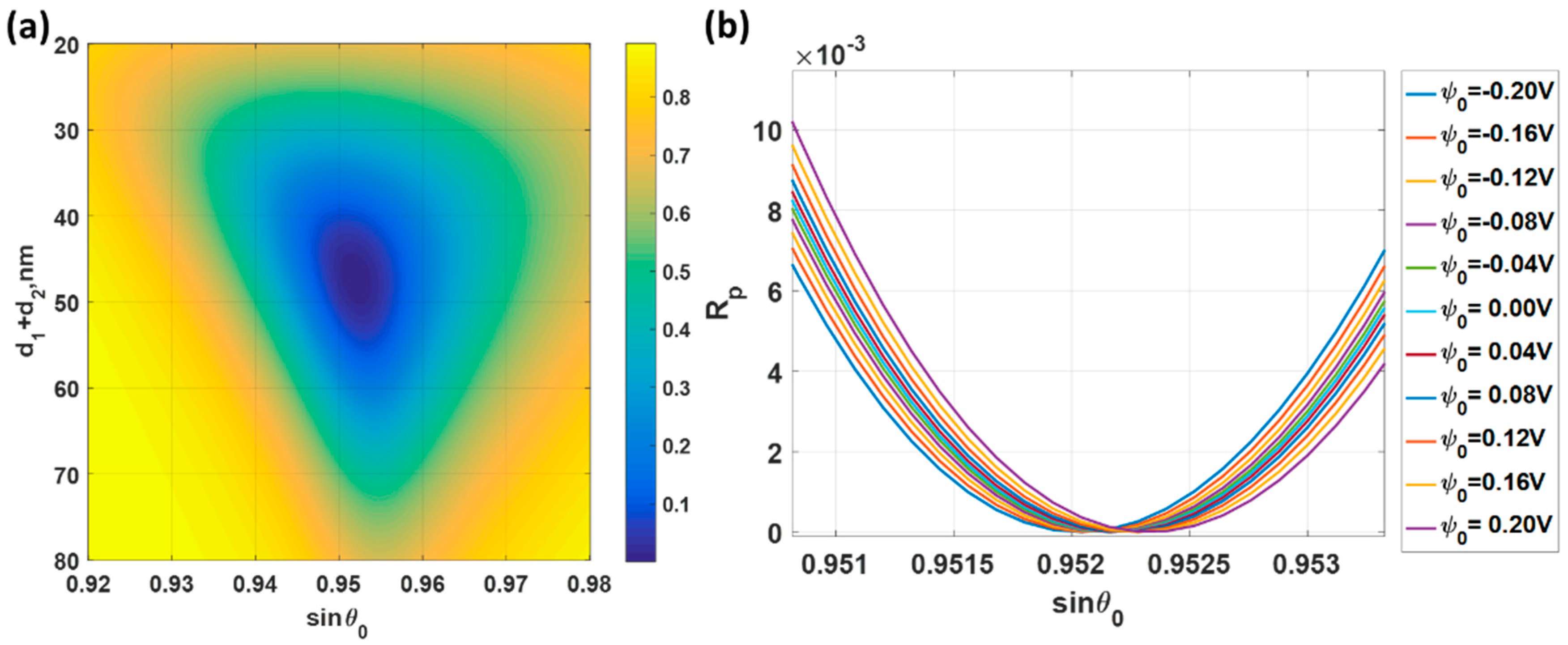
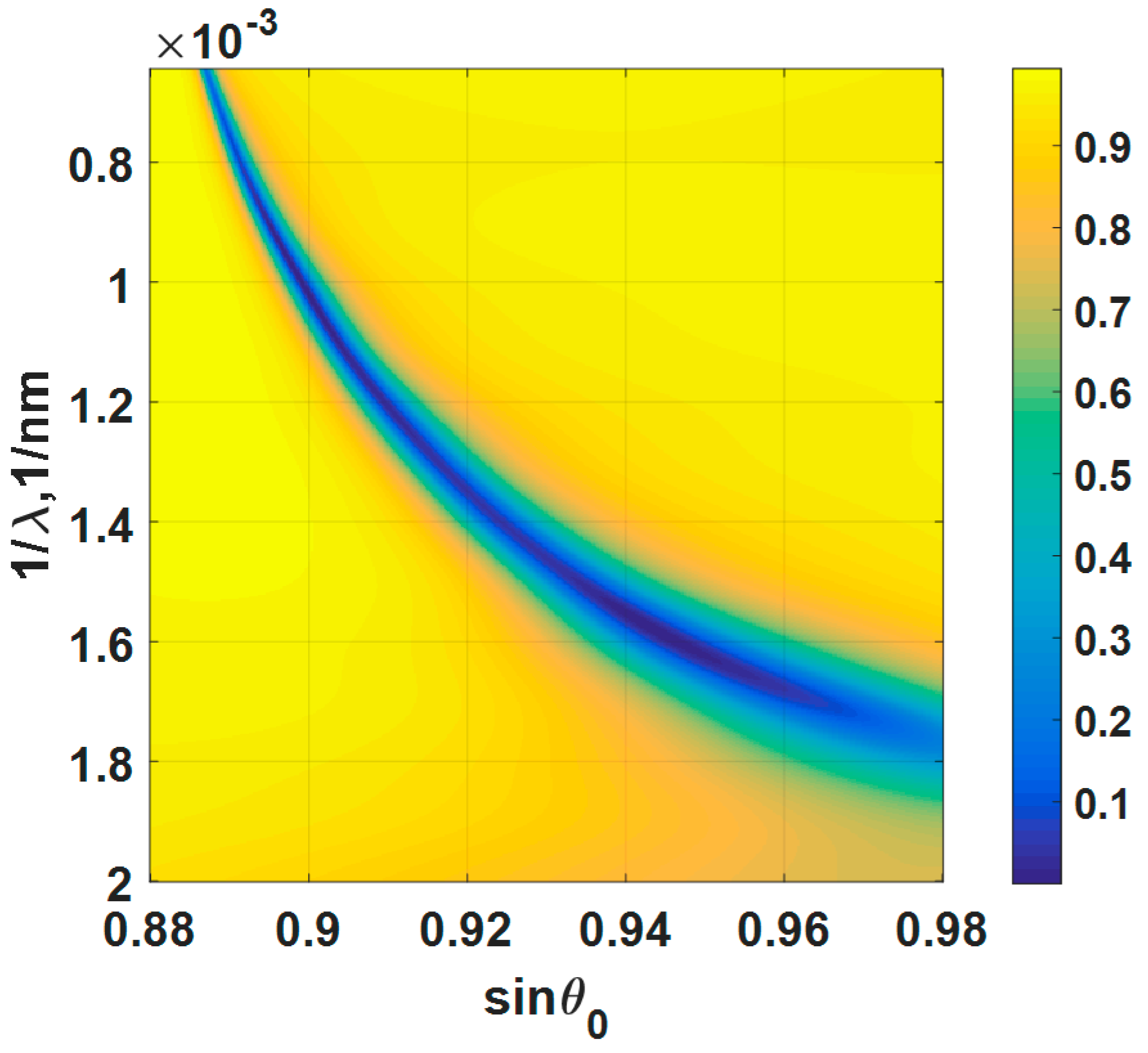
Results for wavelength scanning systems in optics are usually expressed in incident wavelength, λ. Here, the results for wavelength scanning were expressed as 1/λ, which was a linear function of the wave vector. We will show later that by expressing the results in wave vector, this allowed us to compare the performance across different detection mechanisms. The gold thickness of 47 nm has also been employed in this analysis and the refractive indies of the gold for each incident wavelength λ were extracted from Johnson and Christy 1972 [7]. Figure 9a shows reflectance spectra of different incident angles and incident wavelengths, when the 47 nm gold sensor was biased with of 0 V. The lower operating angle gives a narrow full width half maximum spectra. Figure 9b shows reflectance spectra of 47 nm gold sensor for different applied potentials when the incident angle was fixed at sinθ0 of 0.9. The responses like Figure 9b were also calculated for sinθ0 of 0.92, 0.94 and 0.96, but they are omitted to shorten down the length of the manuscript.
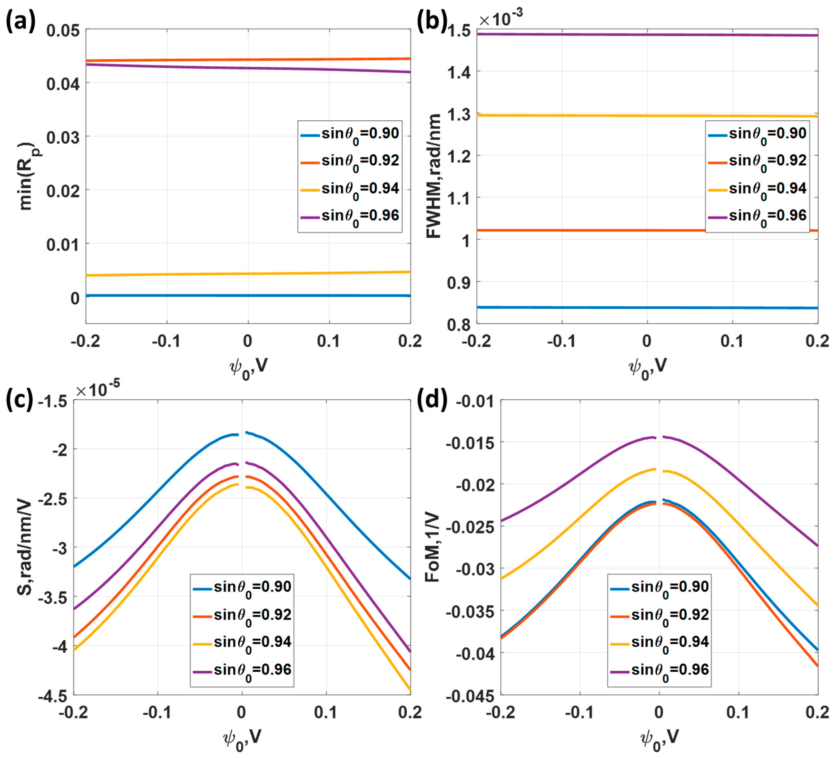
Figure 10a shows the minimum reflectance levels for different incident angle sinθ0 varying from 0.90 to 0.96. The minimum reflectance for all the cases was less than 3.5% level, indicating that the ranges can provide a decent SPR dip response. However, the FWHM does vary by the operating angle as shown in Figure 10b. The lower operating angle sinθ0 has a lower FWHM compared to bigger operating angle cases. The FWHM of the sinθ0 of 0.90 case was 1.5 times narrower than the sinθ0 of 0.96 case. It is interesting to point out that the sensitivity was not the same for all cases and did not vary linearly by the operating angle sinθ0 position. The highest sensitivity of 4.51 × 10⁻⁵ rad/nm/V occurred at sinθ0 of 0.94 and the lowest sensitivity of 3.37 × 10⁻⁵ rad/nm/V was the operating angle of sinθ0 of 0.90. Although the FWHM for the sinθ0 of 0.90 came up as the best performance, the sensitivity for the sinθ0 of 0.90 appeared to be the worst in this simulation set. Since the same performance parameters were used in M1 and M2, this allows us to make a direct comparison between the two sensing mechanisms. The sensitivity for this wavelength scanning system was much higher than the angular scanning system by almost a factor of four, as shown in Figure 10c in comparison with Figure 8c. On the one hand, the FWHM for the wavelength scanning cases were almost 3 to 4 times wider than the FWHM for the angular scanning case as shown in Figure 10b in comparison with Figure 8b. This superior sensitivity for the wavelength scanning system was then cancelled out by the FWHM in the FoM. The FoM of 0.0230 V−1 for the wavelength scanning was slightly worse than the FoM of 0.0244 V−1 of angular scanning case as shown in Figure 10d in comparison with Figure 8d. The FoM in Figure 10d indicates that it is better to setup the SPR platform at a lower incident angle for the wavelength scanning system. Note that the negative values of the sensitivity and the FoM indicate that the SPR dip movement moved in the opposite direction to the M1. For M1 the increased as the applied voltage increased; whereas for M2, the decreased as the applied voltage increased.
It is worth pointing out that some of the measurement mechanisms do not rely on the intensity of the dip, but rely mostly on how much the dip moves, such as interferometric detection [14]. If these techniques were implemented, it is therefore better to align the optical system for wavelength coupling measurement since it has the higher sensitivity compared to angular measurement.
3.1.3. Measurement Mechanism 3 (M3)
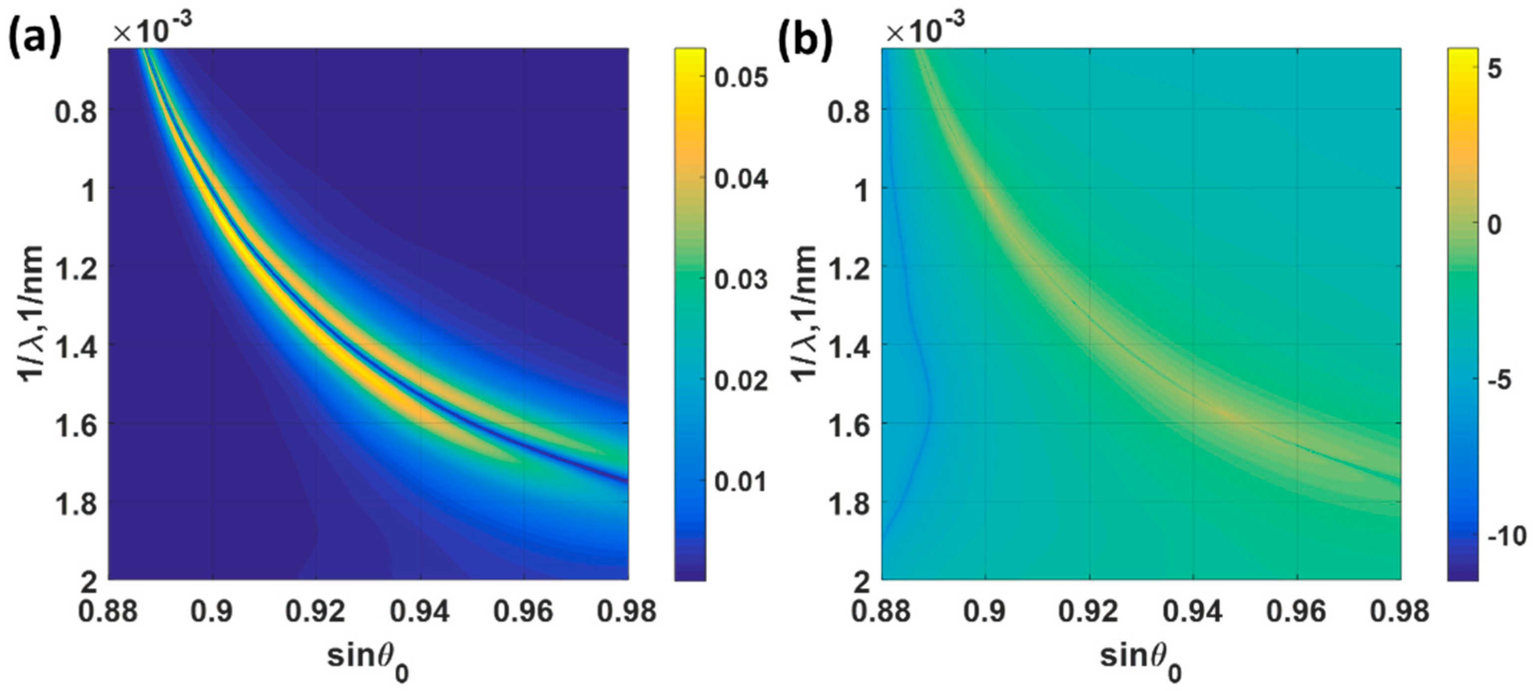
In this section, the optimum thickness of 47 nm is also employed. To calculate the FoM for M3, a set of calculations for the same incident wavelengths and angles as shown in Figure 9a were calculated; however, this time with the applied voltage of 0.2 V. The reflectance spectra shown in Figure 11a allow us to calculate the sensitivity as shown in Figure 11b. The FoM was then calculated by Equation (8) and is shown in Figure 11c. Note that the FoM in Figure 11c is shown in logarithmic base 10 scale for clarity. The maximum FoM of 2735 V−1 occurred at the incident angle sinθ0 of 0.90 and incident wavelength λ of 698.8 nm as highlighted by the arced circle in Figure 11. We will later see that these FoM values can be enhanced further by the bimetallic layer. Table 1 summarizes the performance parameters for the discussed uniform gold SPR sensors.
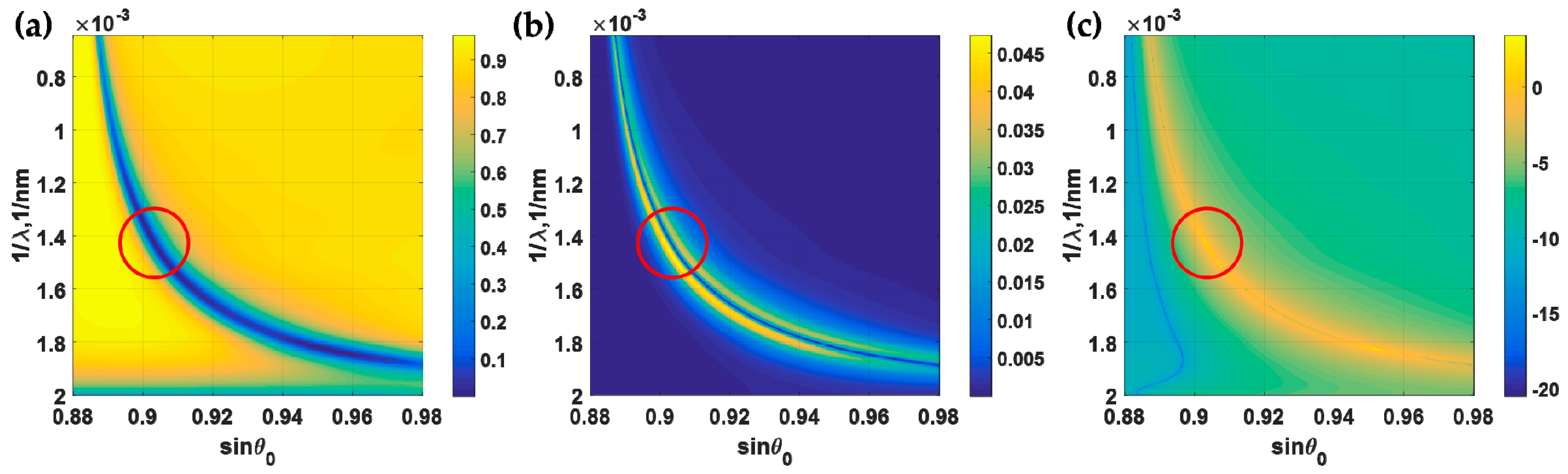
Figure 11b shows us that the maximum sensitivity was around 0.0474. This occurred at sinθ0 of 0.9042 and λ of 898.5 nm. This operating position had the minimum Rp of 0.2659. This sensitivity and this Rp gave 0.1783 S/Rp ratio. The S/Rp is sensitivity per input power. This was a lot lower than the S/Rp of the operating points shown in Table 1, M3. Nowadays, there are a wide variety of high power light sources, however, the fundamental sensitivity per unit power cannot be changed. This is the reason why we defined the performance parameter as sensitivity per unit power.
The S/Rp cannot be directly compared with the FoM for M1 and M2. The FoM performance for M1 and M2 were very similarly around 0.023 to 0.024. Under the condition that FoM performance for angular scanning and wavelength scanning were very similar, it has enabled us to confidently believe that the FoM for M3 mechanism should give a similar FoM response, since for M3 the incident angle and wavelength were fixed. The normalization factor, α, was then introduced by normalizing the FoM of M3 to 0.0244 value by a normalization factor, α 0.0244/15,500 or 1.5742 × 10⁻⁶.
3.2. Bimetallic Layer for Voltage Sensing
Huang et al. [20] proposed a bimetallic layered structure consisting of a silver layer coated by a uniform gold layer wrapping around an optical fiber core. It is important to point out that the bimetallic layer structure proposed by Huang et al. [20] was a bimetallic layer coated on an optical fiber core. The sensitivity depended on the amount of transmission through the fiber, in other words, the SPR detection mechanism was the amount of light absorption in the metal. In this section, we consider only the thin film bimetallic structure as shown in Figure 4. The thin film is applicable for in vitro SPR microscopic sensing [15,21,22,23,24]. Here, the gold layer was in contact with the 0.15 M NaCl electrolytic solution, since the gold is chemically stable and inactive [25,26] whereas silver is highly reactive and can also form hazardous substances [27], such as, silver sulfide Ag2S. The thicknesses of the silver and gold layers considered in this paper were at least 15 nm thick due to two major reasons. Firstly, a very thin layer of gold and silver usually form some defects and islands [28]. The second issue is that all the simulations presented in this manuscript the plasmonic materials were treated as bulk gold. There are several papers reported that there are abnormal transmission spectra when the gold layer and silver layer are thinner than 15 nm [29,30].
3.2.1. Measurement Mechanism 1 (M1)
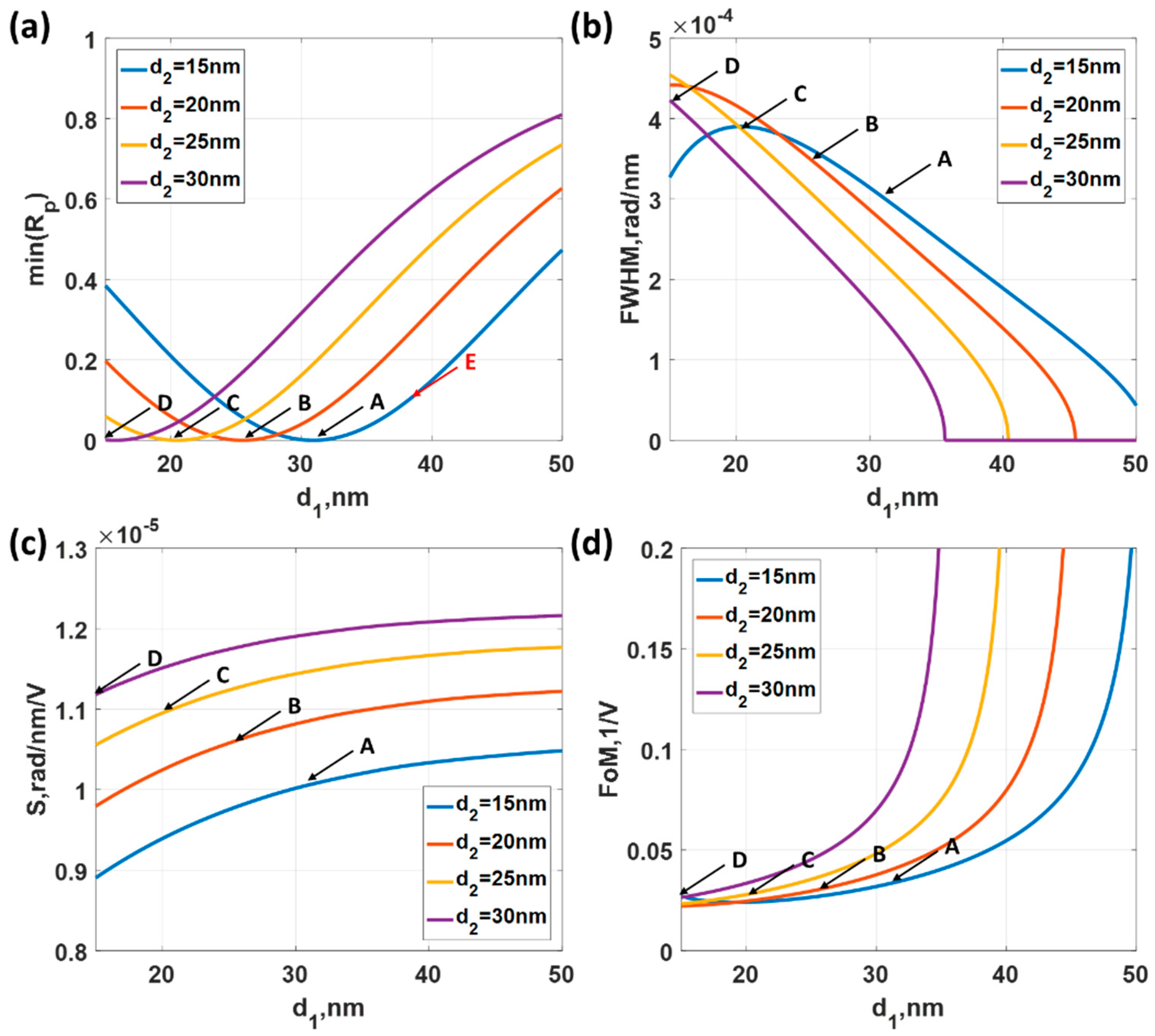
Figure 12a shows the minimum intensity of the reflectance spectra when the thickness of silver d1 was varied from 15 nm to 50 nm and the thickness of gold d2 was 15 nm, 20 nm, 25 nm and 30 nm. The minimum reflectance occurred when the total thickness of d1 and d2 was around 46 nm as labelled by ‘A’, ‘B’, ‘C’ and ‘D’ in Figure 12a. The FWHM for the silver layer is usually narrower than the gold layer, the bilayer structure with thicker layer of silver compared to the gold layer had a lower FWHM as shown in Figure 12b. The label ‘A’ had the narrowest FWHM followed by ‘B’, ‘C’ and ‘D’, respectively. However, the sensitivity had an opposite trend to the FWHM. The narrowest FWHM had the lowest sensitivity and the worst FWHM had the best sensitivity as shown in Figure 12c. The opposite trend of FWHM and the sensitivity, of course, cancelled out in the FoM.
It is important to point out that if the sensitivity or how far the plasmonic dip moves is more important than the depth of the SPR dip. This is the case for the confocal surface plasmon microscopy system [15,21,22] and SPR phase measurements [13,31]. It is then better to operate at slightly higher reflectance intensity as labelled in ‘E’ in Figure 12a. Table 2 summarizes the performance parameters for the bimetallic structure profiles labelled ‘A’ to ‘E’ in Figure 9. In Table 2, it can be seen that the sensitivity performance for the bimetallic layer was slightly worse than the uniform gold sensor case, which was explained in the earlier section. On the other hand, the FWHM of the bimetallic structure was 1.6 times narrower than the uniform gold sensor case. This led to a 1.34 times improvement in FoM of the bimetallic layer compared to the uniform gold sensor case. The bimetallic layer could not enhance the voltage sensing performance much in angular SPR measurement.
3.2.2. Measurement Mechanism 2 (M2)
In this section, we took the structure profile that gave the best performance parameter from M1 section, which is operating point ‘A’: d1 of 31 nm and d2 of 15 nm. Figure 13 shows Rp responses for different incident wavelengths and incident angles. To compare the performance of the bimetallic layered structure and the uniform gold layer in wavelength scanning, the same range of the incident angle sinθ0 of 0.90, 0.92, 0.94 and 0.96 were chosen to calculate the performance parameters as shown in Figure 14. The minimum reflectance at the plasmonic dips were well below 5% for all the cases as shown in Figure 14a. The FWHM was narrower for lower incident angle as shown in Figure 14b. The FWHM for the uniform gold case (see Table 1 measurement 2 for comparison) was two times wider than the bimetallic structure. The sensitivity was also better than the uniform gold case as shown in Figure 14c. This lead to a factor of two enhancement in FoM in wavelength scanning mechanism for the bimetallic structure compared to the uniform gold sample. Table 3 summarizes the performance of the four operating points discussed in this section. This proposed procedure has allowed us to determine what kind of detection mechanism should be implemented for a particular SPR sensing structure. Otherwise, it would not be possible to predict the performance across platform.
3.2.3. Measurement Mechanism 3 (M3)
The FoM for the Measurement mechanism 3 depends on two factors, which are the sensitivity and min(Rp). From Table 2, the lowest min(Rp) value was found in the operating point ‘B’, which was the d1 of 25 nm and d2 of 20 nm case followed by the operating point ‘A’ with the d1 of 31 nm and d2 of the 15 nm case. To calculate the sensitivity and the FoM, Rp responses for the incident angles sinθ0 of 0.88 to 0.98 and incident wavelengths ranging from 500 nm to 1550 nm were simulated with the applied potentials ψ0 of 0 V and 0.2 V for the operating points ‘A’ to ‘D’. The performance parameters are summarized in Table 4. Only the results for operating point ‘B’ are shown in Figure 15. The operating point ‘B’ yielded the best sensitivity and FoM performance compared to the other operating points. The operating point B had the lowest min(Rp) leading to the enhanced FoM of 0.6246, which was 25 times higher than the uniform gold sensor case.
It can be seen from this section that the bimetallic layer could not enhance the FoM for all the detection mechanisms. Mechanism 3 had the highest enhancement in the FoM due to the light intensity absorption mechanism of the bimetallic layer being higher than the single gold layer. Mechanism 2 had a higher FoM enhancement than mechanism 1. This gave us some insights into the SPR behavior that the bimetallic layer enhanced the SPR properties in wavelength domain not the angular domain. It is important to note that without the proposed calculation this would not be obvious to conclude.
4. Conclusions
There are several issues obscuring a direct performance comparison between SPR sensing structures for voltage sensing. Firstly, the electrolytic solution employed in each of the structures was different. Secondly, the SPR measurement mechanisms were different; and thirdly, of course, the sensor structures themselves were also different. In this paper, we have developed a theoretical framework enabling a direct comparison across different SPR platforms based on several performance parameters. We have employed the model developed by Abayzeed et al. and developed it further by defining performance parameters based on wave-vector and sensitivity per input power (S/Rp) and figure of merit (FoM). We demonstrated the proposed concept by analyzing two SPR structures with three SPR detection mechanisms. The analyzed structures were the uniform gold layer and the bimetallic layer consisting of a uniform silver layer coated by another uniform gold layer. The SPR detection mechanisms were M1 to measure the change in the plasmonic coupling angle, M2 to measure the change in the plasmonic coupling wavelength and M3 to measure the change in SP intensity level when the incident angle and incident wavelength were fixed.
For the uniform gold sensor with the optimum thickness of 47 nm, method M2 had a higher sensitivity compared to method M1. The FWHM, however, had an opposite trend. The uniform gold sensor used in method M1 had a narrower FWHM than method M2. These opposite effects therefore cancelled each other out in the FoM calculation. The uniform gold used in method M1 had a slightly better performance than method M2. For method M3, we have discussed the sensitivity per input power and proposed a procedure to normalize the sensitivity per input power to compare with method M1 and M2. The detection mechanisms and the SPR sensor structures should be chosen based on the performance parameters. The sensitivity per input power should be considered for the detection mechanism 3 case without the phase detection technique. On the other hand, the FoM should be considered for detection mechanisms 1 and 2. Note that for detection mechanisms 1 and 2 with phase detection, the sensitivity is more important in these cases.
For the bimetallic layered structure, we have optimized the bimetallic structures for the three SPR measurement mechanisms. This structure did not show much performance improvement in method M1. The optimized structure consisting of 31 nm thick and gold layer of 15 nm thick can only enhance the FoM by 1.34 compared to the uniform gold sensor. On the other hand, method M2 had a better performance than method M1 in terms of the sensitivity, the FWHM and the FoM. In comparison with the uniform gold sensor, the bimetallic sensor had a factor of two improvement in the FoM. For method M3, the optimum thickness of 25.5 nm of silver and 20.0 nm of gold can lead to 25 times improvement in the FoM compared to the uniform gold sensor case.
This analysis has enabled us to not only compare the performance of the different SPR structure and SPR measurement mechanisms, but also to determine which detection mechanism should be implemented to achieve the best performance possible.
Author Contributions
P.S. prepared up the manuscript, analyzed the data, discussed and revised the manuscript; S.P. conceived, designed the analytical calculation, prepared discussed and revised the manuscript.
Funding
This research was funded by Research Institute of Rangsit University grant number 01/2560.
Acknowledgments
The authors would also like to acknowledge Research Institute of Rangsit University for Postdoctoral Fellowships.
Conflicts of Interest
The authors declare no conflict of interest.
References
- Zhang, J.; Atay, T.; Nurmikko, A.V. Optical detection of brain cell activity using plasmonic gold nanoparticles. Nano Lett. 2009, 9, 519–524. [Google Scholar] [CrossRef] [PubMed]
- Haynes, W.M. CRC Handbook of Chemistry and Physics; CRC Press: Boca Raton, FL, USA, 2014. [Google Scholar]
- Davey, W.P. Precision measurements of the lattice const;nts of twelve common metals. Phys. Rev. 1925, 25, 753. [Google Scholar] [CrossRef]
- McIntyre, J.; Aspnes, D.E. Differential reflection spectroscopy of very thin surface films. Surf. Sci. 1971, 24, 417–434. [Google Scholar] [CrossRef]
- Garcia, N.; Damask, A. Physics for Computer Science Students: With Emphasis on Atomic and Semiconductor Physics; Springer Science & Business Media: Berlin, Germany, 2012. [Google Scholar]
- Rakić, A.D.; Djurišić, A.B.; Elazar, J.M.; Majewski, M.L. Optical properties of metallic films for vertical-cavity optoelectronic devices. Appl. Opt. 1998, 37, 5271–5283. [Google Scholar] [CrossRef] [PubMed]
- Johnson, P.B.; Christy, R.-W. Optical constants of the noble metals. Phys. Rev. B 1972, 6, 4370. [Google Scholar] [CrossRef]
- Optical Glass. Available online: https://www.schott.com/advanced_optics/english/products/optical-materials/optical-glass/optical-glass/index.html (accessed on 22 August 2018).
- Hecht, E. Hecht optics. Addison Wesley 1998, 997, 213–214. [Google Scholar]
- Garland, J.; Assiongbon, K.; Pettit, C.; Roy, D. Surface plasmon resonance transients at an electrochemical interface: Time resolved measurements using a bicell photodiode. Anal. Chim. Acta 2003, 475, 47–58. [Google Scholar] [CrossRef]
- Kotnik, T.; Miklavčič, D. Theoretical evaluation of voltage inducement on internal membranes of biological cells exposed to electric fields. Biophys. J. 2006, 90, 480–491. [Google Scholar] [CrossRef] [PubMed]
- Puiu, M.; Bala, C. Spr and spr imaging: Recent trends in developing nanodevices for detection and real-time monitoring of biomolecular events. Sensors 2016, 16, 870. [Google Scholar] [CrossRef] [PubMed]
- Huang, Y.; Ho, H.; Wu, S.; Kong, S.; Wong, W.; Shum, P. Phase sensitive spr sensor for wide dynamic range detection. Opt. Lett. 2011, 36, 4092–4094. [Google Scholar] [CrossRef] [PubMed]
- Suvarnaphaet, P.; Pechprasarn, S. Enhancement of long-range surface plasmon excitation, dynamic range and figure of merit using a dielectric resonant cavity. Sensors 2018, 18, 2757. [Google Scholar] [CrossRef] [PubMed]
- Pechprasarn, S.; Chow, T.W.; Somekh, M.G. Application of confocal surface wave microscope to self-calibrated attenuation coefficient measurement by goos-hänchen phase shift modulation. Sci. Rep. 2018, 8, 8547. [Google Scholar] [CrossRef] [PubMed]
- Abayzeed, S.A.; Smith, R.J.; Webb, K.F.; Somekh, M.G.; See, C.W. Sensitive detection of voltage transients using differential intensity surface plasmon resonance system. Opt. Express 2017, 25, 31552–31567. [Google Scholar] [CrossRef] [PubMed]
- Filion-Côté, S.; Roche, P.J.; Foudeh, A.M.; Tabrizian, M.; Kirk, A.G. Design and analysis of a spectro-angular surface plasmon resonance biosensor operating in the visible spectrum. Rev. Sci. Instrum. 2014, 85, 093107. [Google Scholar] [CrossRef] [PubMed] [Green Version]
- Pechprasarn, S.; Learkthanakhachon, S.; Zheng, G.; Shen, H.; Lei, D.Y.; Somekh, M.G. Grating-coupled otto configuration for hybridized surface phonon polariton excitation for local refractive index sensitivity enhancement. Opt. Express 2016, 24, 19517–19530. [Google Scholar] [CrossRef] [PubMed]
- Moharam, M.; Gaylord, T. Rigorous coupled-wave analysis of planar-grating diffraction. JOSA 1981, 71, 811–818. [Google Scholar] [CrossRef]
- Huang, Y.; Xia, L.; Wei, W.; Chuang, C.-J.; Du, C. Theoretical investigation of voltage sensitivity enhancement for surface plasmon resonance based optical fiber sensor with a bimetallic layer. Opt. Commun. 2014, 333, 146–150. [Google Scholar] [CrossRef]
- Pechprasarn, S.; Somekh, M.G. Detection limits of confocal surface plasmon microscopy. Biomed. Opt. Express 2014, 5, 1744–1756. [Google Scholar] [CrossRef] [PubMed]
- Pechprasarn, S.; Zhang, B.; Albutt, D.; Zhang, J.; Somekh, M. Ultrastable embedded surface plasmon confocal interferometry. Light Sci. Appl. 2014, 3, e187. [Google Scholar] [CrossRef]
- Somekh, M.G.; Pechprasarn, S. Surface plasmon, surface wave, and enhanced evanescent wave microscopy. Handb. Photonics Biomed. Eng. 2016, 1–41. [Google Scholar] [CrossRef]
- Tan, H.-M.; Pechprasarn, S.; Zhang, J.; Pitter, M.C.; Somekh, M.G. High resolution quantitative angle-scanning widefield surface plasmon microscopy. Sci. Rep. 2016, 6, 20195. [Google Scholar] [CrossRef] [PubMed]
- Ferreira de Macedo, E.; Ducatti Formaggio, D.M.; Salles Santos, N.; Batista Tada, D. Gold nanoparticles used as protein scavengers enhance surface plasmon resonance signal. Sensors 2017, 17, 2765. [Google Scholar] [CrossRef] [PubMed]
- Saha, K.; Agasti, S.S.; Kim, C.; Li, X.; Rotello, V.M. Gold nanoparticles in chemical and biological sensing. Chem. Rev. 2012, 112, 2739–2779. [Google Scholar] [CrossRef] [PubMed]
- Drake, P.L.; Hazelwood, K.J. Exposure-related health effects of silver and silver compounds: A review. Ann. Occup. Hyg. 2005, 49, 575–585. [Google Scholar] [PubMed]
- Yakubovsky, D.I.; Arsenin, A.V.; Stebunov, Y.V.; Fedyanin, D.Y.; Volkov, V.S. Optical constants and structural properties of thin gold films. Opt. Express 2017, 25, 25574–25587. [Google Scholar] [CrossRef] [PubMed]
- Azeredo, B.P.; Yeratapally, S.R.; Kacher, J.; Ferreira, P.M.; Sangid, M.D. An experimental and computational study of size-dependent contact-angle of dewetted metal nanodroplets below its melting temperature. Appl. Phys. Lett. 2016, 109, 213101. [Google Scholar] [CrossRef] [Green Version]
- Tu, J.; Homes, C.; Strongin, M. Optical properties of ultrathin films: Evidence for a dielectric anomaly at the insulator-to-metal transition. Phys. Rev. Lett. 2003, 90, 017402. [Google Scholar] [CrossRef] [PubMed]
- Wong, C.L.; Chua, M.; Mittman, H.; Choo, L.X.; Lim, H.Q.; Olivo, M. A phase-intensity surface plasmon resonance biosensor for avian influenza a (h5n1) detection. Sensors 2017, 17, 2363. [Google Scholar] [CrossRef] [PubMed]
Figure 1.
Illustration of (a) a uniform plasmonic gold sample; (b) bimetallic layers of gold (Au) and silver (Ag) wrapping around the fiber optic core.
Figure 1.
Illustration of (a) a uniform plasmonic gold sample; (b) bimetallic layers of gold (Au) and silver (Ag) wrapping around the fiber optic core.

Figure 2.
Voltage potential profile using Gouy-Chapman-Stern model. The Stern potential was calculated for the applied voltage of 0.1 V and the electrolyte was 0.15 M NaCl solution.
Figure 2.
Voltage potential profile using Gouy-Chapman-Stern model. The Stern potential was calculated for the applied voltage of 0.1 V and the electrolyte was 0.15 M NaCl solution.

Figure 3.
Simplified model for uniform gold SPR sensor consisting of the charged Thomas-Fermi screening length of 0.5 Å and the uniform bulk gold layer.
Figure 3.
Simplified model for uniform gold SPR sensor consisting of the charged Thomas-Fermi screening length of 0.5 Å and the uniform bulk gold layer.

Figure 4.
Simplified model for bimetallic SPR sensor consisting of a uniform silver layer and two gold layers, which consists of a uniform bulk gold layer and the top gold layer is the charged Thomas-Fermi screening length of 0.5 Å.
Figure 4.
Simplified model for bimetallic SPR sensor consisting of a uniform silver layer and two gold layers, which consists of a uniform bulk gold layer and the top gold layer is the charged Thomas-Fermi screening length of 0.5 Å.

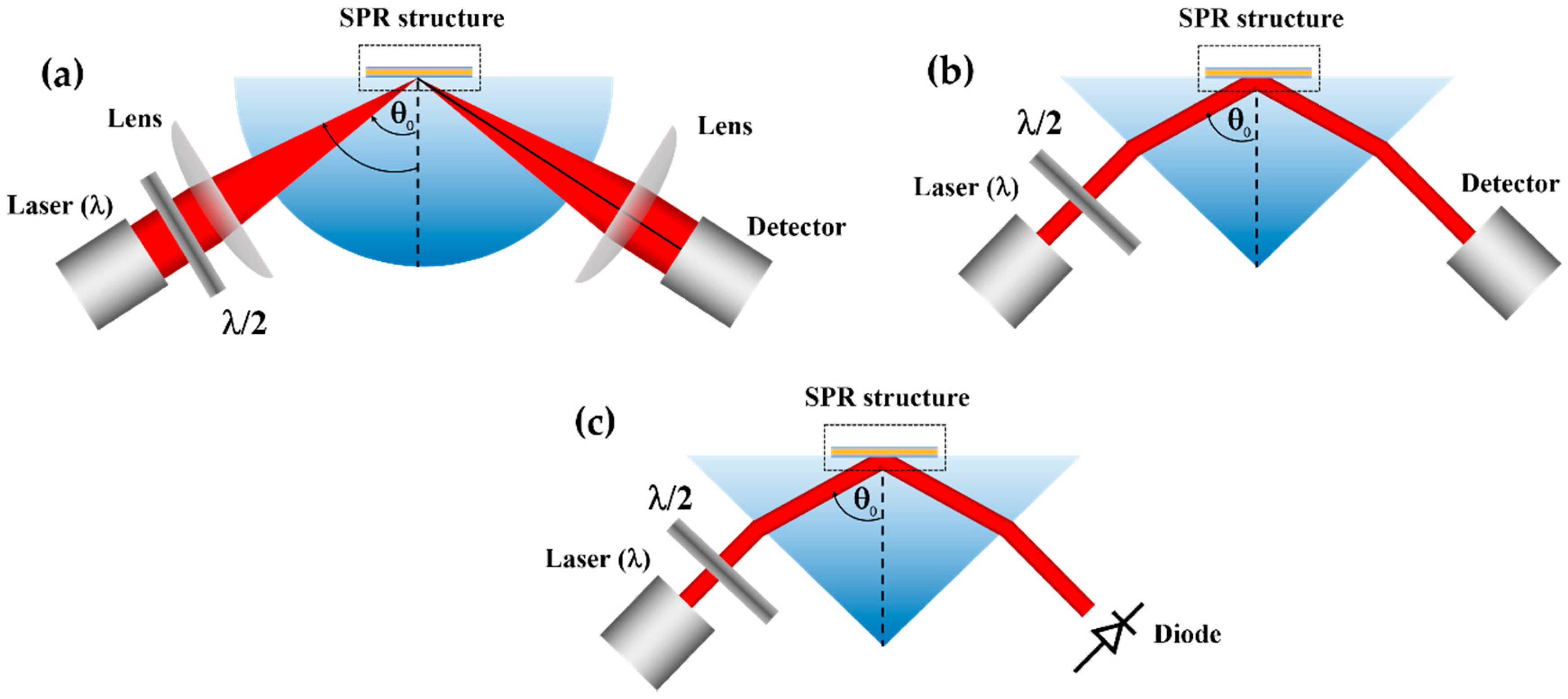
Figure 5.
Illustration of SPR sensing structure based on Kretschmann configurations for (a) M1, (b) M2, and (c) M3.
Figure 5.
Illustration of SPR sensing structure based on Kretschmann configurations for (a) M1, (b) M2, and (c) M3.

Figure 6.
Illustrations showing how the parameters were measured. Rp response for of 0 V (solid black curve) and Rp response for greater than 0 V (solid red curve).
Figure 6.
Illustrations showing how the parameters were measured. Rp response for of 0 V (solid black curve) and Rp response for greater than 0 V (solid red curve).

Figure 7.
(a) Rp responses for different incident angles ranging from 0.92 to 0.98. The applied potential of 0 V was applied at the incident wavelength λ of 632.8 nm; (b) Rp responses when different voltage levels were applied. The responses were simulated with the total gold thickness of 47 nm and the incident wavelength λ of 632.8 nm.

Figure 8.
Responses of the 47 nm thick uniform gold sensor for different applied potential levels ranging from −0.2 V to 0.2 V and the incident wavelength λ of 632.8 nm includes (a) minimum reflectance intensity level at the plasmonic angles min (Rp); (b) full width half maximum; (c) sensitivity; and (d) Figure of Merit.

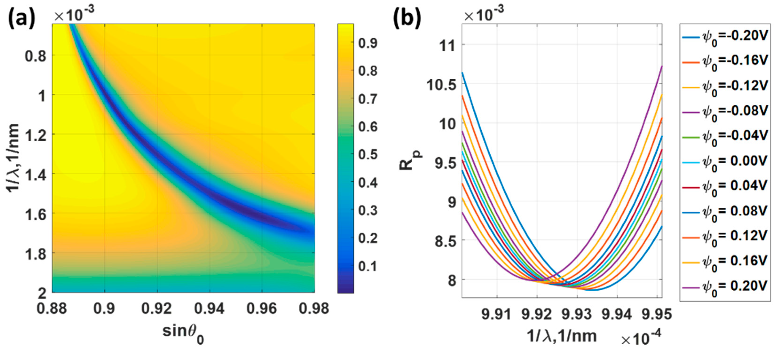
Figure 9.
(a) Reflectance spectra of different incident angles ranging from 0.88 to 0.98 and incident wavelengths ranging from 500 nm to 1550 nm, when the 47 nm gold sensor was biased with of 0 V. (b) Reflectance spectra of 47 nm gold sensor for different applied potentials when the incident angle was fixed at sinθ0 of 0.9.

Figure 10.
Responses of the 47 nm thick uniform gold sensor for different applied potential levels ranging from −0.2 V to 0.2 V and the incident angles of sinθ0 of 0.90, 0.92, 0.94 and 0.96. (a) Minimum reflectance intensity level at the plasmonic wavelengths min(Rp); (b) full width half maximum; (c) Sensitivity; and (d) Figure of Merit.

Figure 11.
(a) Reflectance spectra of different incident angles and incident wavelengths, when the 47 nm gold sensor was biased with ψ0 of 0.2 V. (b) Sensitivity for M3 calculated using Figure 9a and Figure 11a,c. (c) FoM, calculated using Equation (8). Red arced circles highlight the maximum FoM.

Figure 12.
Performance parameters calculated by varying silver layer thickness d1 from 15 nm to 50 nm and gold thickness d2 of 15 nm (solid blue curve), 20 nm (solid red curve), 25 nm (solid yellow curve) and 30 nm (solid purple curve) when the incident wavelength λ was fixed at 632.8 nm and the applied potential ψ0 of 0 V at (a) minimum Rp; (b) FWHM. (c) Sensitivity calculated by comparing the plasmonic wave vector positions of applied potentials ψ0 of 0 V and 0.2 V and (d) FoM calculated from Figure 12b,c.

Figure 13.
Reflectance spectrum of different incident angles and incident wavelengths, when the bimetallic layer consisting of a silver layer 31 nm thick and a gold layer 15 nm thick with the external applied potential ψ0 of 0 V.
Figure 13.
Reflectance spectrum of different incident angles and incident wavelengths, when the bimetallic layer consisting of a silver layer 31 nm thick and a gold layer 15 nm thick with the external applied potential ψ0 of 0 V.

Figure 14.
Responses when the bimetallic layer consisting of a silver layer 31 nm thick and a gold layer 15 nm thick for different applied potential levels ranging from −0.2 V to 0.2 V and the incident angles of sinθ0 of 0.90, 0.92, 0.94 and 0.96. (a) Minimum reflectance intensity level at the plasmonic wavelengths min(Rp); (b) full width half maximum; (c) Sensitivity; and (d) Figure of Merit.

Figure 15.
(a) Sensitivity (S) for mechanism 3 and (b) FoM calculated using Equation (8) with the structure profile of the operating point ‘B’ d1 of 25 nm and d2 of 20 nm. The sensitivity and FoM were calculated from Rp responses of the biased voltage ψ0 of 0 V to 0.2 V.
Figure 15.
(a) Sensitivity (S) for mechanism 3 and (b) FoM calculated using Equation (8) with the structure profile of the operating point ‘B’ d1 of 25 nm and d2 of 20 nm. The sensitivity and FoM were calculated from Rp responses of the biased voltage ψ0 of 0 V to 0.2 V.


Table 1.
Summarizes the performance parameters for 47 nm thick uniform gold SPR sensors.
| SPR Measurement Mechanism 1 | |||||
| Incident wavelength λ (nm) | Plasmonic angle sinθsp | Min(Rp) | FWHM (rad/nm) | Sensitivity (S) rad/nm/V | Figure of Merit (FoM) 1/V |
| 632.8 | 0.9522 | 1.10 × 10⁻⁶ | 4.75 × 10⁻⁴ | 1.16 × 10⁻⁵ | 0.0244 |
| SPR Measurement Mechanism 2 | |||||
| Plasmonic wavelength λSP (nm) | Incident angle sinθ0 | Min(Rp) | FWHM (rad/nm) | Sensitivity (S) rad/nm/V | Figure of Merit (FoM) 1/V |
| 1008.0 | 0.9000 | 7.99 × 10⁻³ | 15.59 ×10⁻⁴ | 3.37 × 10⁻⁵ | 0.0216 |
| 766.7 | 0.9200 | 27.24 × 10⁻³ | 18.84 ×10⁻⁴ | 4.24 × 10⁻⁵ | 0.0230 |
| 665.9 | 0.9400 | 32.61 × 10⁻³ | 21.26 ×10⁻⁴ | 4.51 × 10⁻⁵ | 0.0212 |
| 615.5 | 0.9600 | 9.35 × 10⁻³ | 23.26 ×10⁻⁴ | 3.86 × 10⁻⁵ | 0.0166 |
| SPR Measurement Mechanism 3 | |||||
| Incident wavelength λ (nm) | Incident angle sinθ0 | Rp | Sensitivity (S) 1/V | S/Rp | Figure of Merit (FoM) 1/V |
| 941.2 | 0.9034 | 6.14 × 10⁻⁸ | 9.52 × 10⁻⁴ | 15,500 | 0.0244 |
Table 2.
Summarizes the performance parameters bimetallic layered structures for angular measurement mechanism.
Table 2.
Summarizes the performance parameters bimetallic layered structures for angular measurement mechanism.
| SPR Measurement Mechanism 1 | ||||||||
|---|---|---|---|---|---|---|---|---|
| Operating point | Silver thickness (d1) nm | Gold thickness (d2) nm | Incident wavelength λ (nm) | Plasmonic angle sinθsp | Min(Rp) | FWHM rad/nm | Sensitivity (S) rad/nm/V | Figure of Merit (FoM) 1/V |
| ‘A’ | 31.0 | 15.0 | 632.8 | 0.9435 | 2.84 × 10⁻⁷ | 3.02 × 10⁻⁴ | 1.00 × 10⁻⁵ | 0.0333 |
| ‘B’ | 25.5 | 20.0 | 632.8 | 0.9464 | 8.33 × 10⁻⁸ | 3.50 × 10⁻⁴ | 1.06 × 10⁻⁵ | 0.0303 |
| ‘C’ | 20.5 | 25.0 | 632.8 | 0.9485 | 1.52 × 10⁻⁶ | 3.86 × 10⁻⁴ | 1.10 × 10⁻⁵ | 0.0285 |
| ‘D’ | 15.8 | 30.0 | 632.8 | 0.9500 | 2.03 × 10⁻⁶ | 4.11 × 10⁻⁴ | 1.12 × 10⁻⁵ | 0.0273 |
| ‘E’ | 38.2 | 15.0 | 632.8 | 0.9509 | 0.1 | 2.11 × 10⁻⁴ | 1.03 × 10⁻⁵ | 0.0488 |
Table 3.
Summarizes the performance parameters bimetallic layered structure with d1 of 31 nm and d2 of 15 nm for plasmonic wavelength measurement.
Table 3.
Summarizes the performance parameters bimetallic layered structure with d1 of 31 nm and d2 of 15 nm for plasmonic wavelength measurement.
| SPR Measurement Mechanism 2 | |||||||
|---|---|---|---|---|---|---|---|
| Silver thickness (d1) nm | Gold thickness (d2) nm | Plasmonic wavelength λSP (nm) | Incident angle sinθ0 | Min(Rp) | FWHM rad/nm | Sensitivity (S) rad/nm/V | Figure of Merit (FoM) 1/V |
| 31.0 | 15.0 | 981.4 | 0.90 | 2.38 × 10⁻⁴ | 8.37 × 10⁻⁴ | 3.33 × 10⁻⁵ | 0.0397 |
| 31.0 | 15.0 | 740.7 | 0.92 | 4.44 × 10⁻² | 10.21 × 10⁻⁴ | 4.25 × 10⁻⁵ | 0.0416 |
| 31.0 | 15.0 | 643.9 | 0.94 | 4.45 × 10⁻³ | 12.39 × 10⁻⁴ | 4.45 × 10⁻⁵ | 0.0347 |
| 31.0 | 15.0 | 595.2 | 0.96 | 4.28 × 10⁻² | 14.85 × 10⁻⁴ | 4.07 × 10⁻⁵ | 0.0274 |
Table 4.
Summarizes the performance parameters bimetallic layered structures with different d1 and d2 for mechanism 3 measurement.
Table 4.
Summarizes the performance parameters bimetallic layered structures with different d1 and d2 for mechanism 3 measurement.
| SPR Measurement Mechanism 3 | ||||||||
|---|---|---|---|---|---|---|---|---|
| Operating point | Silver thickness (d1) nm | Gold thickness (d2) nm | Incident wavelength λ(nm) | Incident angle sinθ0 | Rp | Sensitivity (S) 1/V | S/Rp | Figure of Merit (FoM) 1/V |
| ‘A’ | 31.0 | 15.0 | 994.5 | 0.8994 | 4.30 × 10⁻⁷ | 14.23 × 10⁻⁴ | 3306 | 0.0052 |
| ‘B’ | 25.5 | 20.0 | 632.9 | 0.9464 | 1.89 × 10⁻⁹ | 7.48 × 10⁻⁴ | 396,777 | 0.6246 |
| ‘C’ | 20.5 | 25.0 | 965.9 | 0.9016 | 1.79 × 10⁻⁸ | 9.04 × 10⁻⁴ | 50,556 | 0.0796 |
| ‘D’ | 15.8 | 30.0 | 814.5 | 0.9130 | 9.96 × 10⁻⁷ | 10.86 × 10⁻⁴ | 1,090 | 0.0017 |
© 2018 by the authors. Licensee MDPI, Basel, Switzerland. This article is an open access article distributed under the terms and conditions of the Creative Commons Attribution (CC BY) license (http://creativecommons.org/licenses/by/4.0/).
Share and Cite
MDPI and ACS Style
Suvarnaphaet, P.; Pechprasarn, S. Quantitative Cross-Platform Performance Comparison between Different Detection Mechanisms in Surface Plasmon Sensors for Voltage Sensing. Sensors 2018, 18, 3136. https://doi.org/10.3390/s18093136
AMA Style
Suvarnaphaet P, Pechprasarn S. Quantitative Cross-Platform Performance Comparison between Different Detection Mechanisms in Surface Plasmon Sensors for Voltage Sensing. Sensors. 2018; 18(9):3136. https://doi.org/10.3390/s18093136
Chicago/Turabian StyleSuvarnaphaet, Phitsini, and Suejit Pechprasarn. 2018. "Quantitative Cross-Platform Performance Comparison between Different Detection Mechanisms in Surface Plasmon Sensors for Voltage Sensing" Sensors 18, no. 9: 3136. https://doi.org/10.3390/s18093136
Note that from the first issue of 2016, this journal uses article numbers instead of page numbers. See further details here.