High-Performance Photoresistors Based on Perovskite Thin Film with a High PbI2 Doping Level


Abstract
:
1. Introduction
2. Materials and Methods
2.1. Materials and Preparation of Perovskite Precursor Solution
2.2. Fabrication of the Devices
2.3. Characterization of Perovskite Thin Films and Device Performance
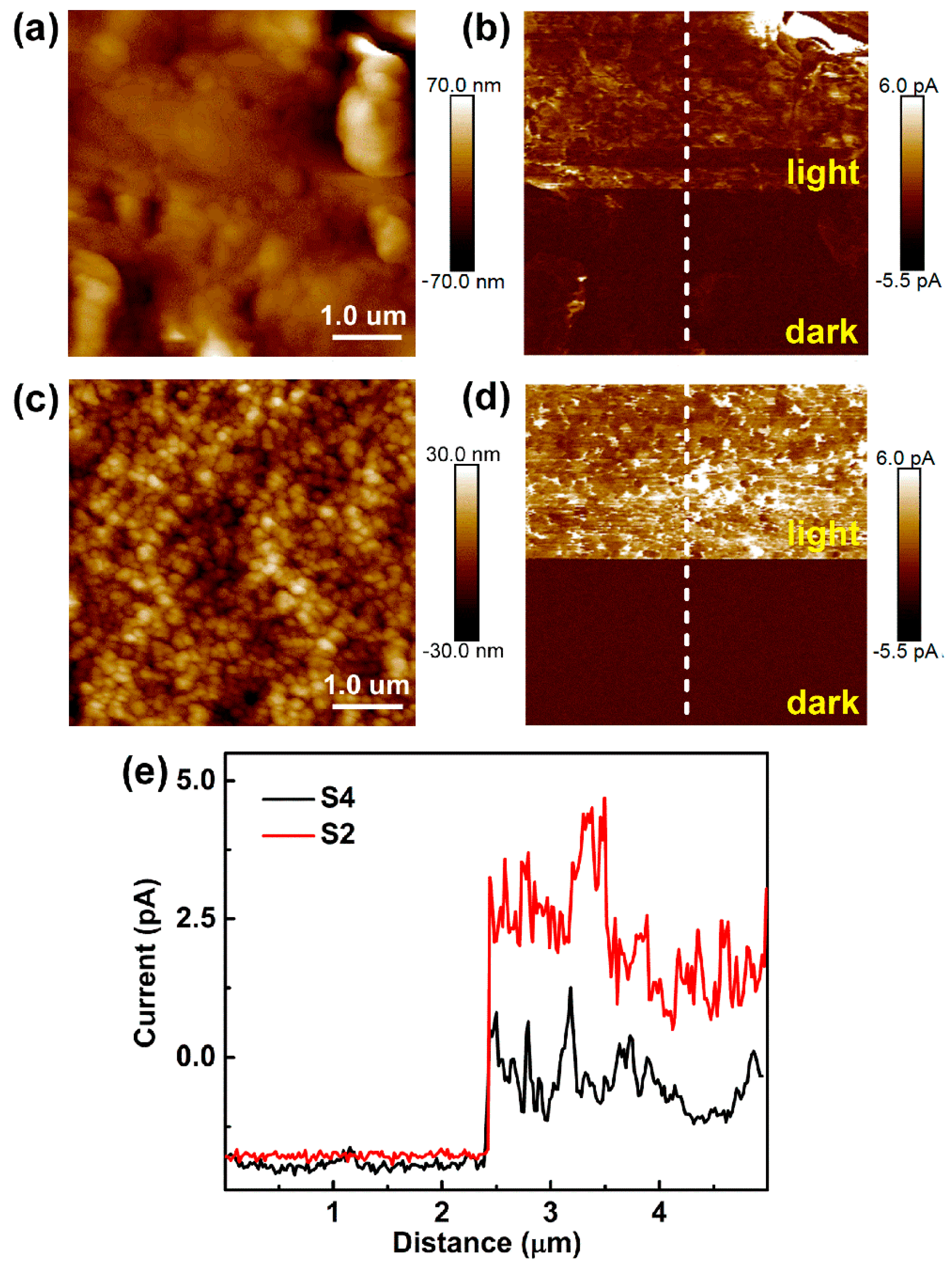
3. Results and Discussion
4. Conclusions
Supplementary Materials
Author Contributions
Funding
Conflicts of Interest
References
- Kojima, A.; Teshima, K.; Shirai, Y.; Miyasaka, T. Organometal Halide Perovskites as a visible light sensitizers for photovoltaic cells. J. Am. Chem. Soc. 2009, 131, 6050–6051. [Google Scholar] [CrossRef] [PubMed]
- Stranks, S.D.; Snaith, H.J. Metal-halide perovskites for photovoltaic and light-emitting devices. Nat. Nanotechnol. 2015, 10, 391–402. [Google Scholar] [CrossRef] [PubMed]
- Green, M.A.; Baillie, A.H.; Snaith, H.J. The emergence of perovskite solar cells. Nat. Photonics 2014, 8, 506–514. [Google Scholar] [CrossRef]
- Eperon, G.E.; Hörantner, M.T.; Snaith, H.J. Metal halide perovskite tandem and multiple-junction photovoltaics. Nat. Rev. Chem. 2017, 1, 0095. [Google Scholar] [CrossRef]
- Snaith, H.J.; Lilliu, S. The Path to Perovskite on Silicon PV. Sci. Video Protoc. 2018, 1, 1. [Google Scholar] [CrossRef]
- Liu, M.; Johnston, M.B.; Snaith, H.J. Efficient planar heterojunction perovskite solar cells by vapour deposition. Nature 2013, 501, 395–398. [Google Scholar] [CrossRef]
- Arora, N.; Dar, M.I.; Hinderhofer, A.; Pellet, N.; Schreiber, F.; Zakeeruddin, S.M.; Gratzel, M. Perovskite solar cells with CuSCN hole extraction layers yield stabilized efficiencies greater than 20%. Science 2017, 358, 768–771. [Google Scholar] [CrossRef] [Green Version]
- Wang, Y.; Zhang, Y.; Lu, Y.; Xu, W.; Mu, H.; Chen, C.; Qiao, H.; Song, J.; Li, S.; Sun, B.; et al. Hybrid Graphene-Perovskite Phototransistors with Ultrahigh Responsivity and Gain. Adv. Opt. Mater. 2015, 3, 1389–1396. [Google Scholar] [CrossRef]
- Yu, Y.; Zhang, Y.; Zhang, Z.; Zhang, H.; Song, X.; Cao, M.; Che, Y.; Dai, H.; Yang, J.; Wang, J.; et al. Broadband Phototransistor Based on CH3NH3PbI3 Perovskite and PbSe Quantum Dot Heterojunction. J. Phys. Chem. Lett. 2017, 8, 445–451. [Google Scholar] [CrossRef] [PubMed]
- Wang, W.; Ma, Y.; Qi, L.; Ding, J.; Fang, H.; Lian, Z.; Li, J.; Lv, Q.; Wang, L.; Sun, J.; et al. A self-powered photodetector based on a CH3NH3PbI3 single crystal with asymmetric electrodes. CrystEngComm 2016, 18, 4405–4411. [Google Scholar]
- Ma, C.; Shi, Y.; Hu, W.; Chiu, M.H.; Liu, Z.; Bera, A.; Li, F.; Wang, H.; Li, L.J.; Wu, T. Heterostructured WS2/CH3 NH3 PbI3 Photoconductors with Suppressed Dark Current and Enhanced Photodetectivity. Adv. Mater. 2016, 28, 3683–3689. [Google Scholar] [CrossRef]
- Su, L.; Zhao, Z.; Li, H.; Yuan, J.; Wang, Z.; Cao, G.; Zhu, G. High performance organolead halide perovskite based self-powered triboelectric photodetector. ACS Nano 2015, 9, 11310–11316. [Google Scholar] [CrossRef]
- Lu, H.; Tian, W.; Cao, F.; Ma, Y.; Gu, B.; Li, L. A Self-Powered and Stable All-Perovskite Photodetector-Solar Cell Nanosystem. Adv. Funct. Mater. 2016, 26, 1296–1302. [Google Scholar] [CrossRef]
- Lee, W.; Lee, J.; Yun, H.; Kim, J.; Park, J.; Choi, C.; Kim, D.C.; Seo, H.; Lee, H.; Yu, J.W.; et al. High-Resolution Spin-on-Patterning of Perovskite Thin Films for a Multiplexed Image Sensor Array. Adv. Mater. 2017, 29, 1702902. [Google Scholar] [CrossRef]
- Gu, L.; Tavakoli, M.M.; Zhang, D.; Zhang, Q.; Waleed, A.; Xiao, Y.; Tsui, K.H.; Lin, Y.; Liao, L.; Wang, J.; et al. 3D Arrays of 1024-Pixel Image Sensors based on Lead Halide Perovskite Nanowires. Adv. Mater. 2016, 28, 9713–9721. [Google Scholar] [CrossRef]
- Deng, W.; Zhang, X.; Huang, L.; Xu, X.; Wang, L.; Wang, J.; Shang, Q.; Lee, S.T.; Jie, J. Aligned Single-Crystalline Perovskite Microwire Arrays for High-Performance Flexible Image Sensors with Long-Term Stability. Adv. Mater. 2016, 28, 2201–2208. [Google Scholar] [CrossRef]
- Wei, H.; Fang, Y.; Mulligan, P.; Chuirazzi, W.; Fang, H.-H.; Wang, C.; Ecker, B.R.; Gao, Y.; Loi, M.A.; Cao, L.; et al. Sensitive X-ray detectors made of methylammonium lead tribromide perovskite single crystals. Nat. Photonics 2016, 10, 333–339. [Google Scholar] [CrossRef]
- Yakunin, S.; Sytnyk, M.; Kriegner, D.; Shrestha, S.; Richter, M.; Matt, G.J.; Azimi, H.; Brabec, C.J.; Stangl, J.; Kovalenko, M.V.; et al. Detection of X-ray photons by solution-processed organic-inorganic perovskites. Nat. Photonics 2015, 9, 444–449. [Google Scholar] [CrossRef] [Green Version]
- Birowosuto, M.D.; Cortecchia, D.; Drozdowski, W.; Brylew, K.; Lachmanski, W.; Bruno, A.; Soci, C. X-ray Scintillation in Lead Halide Perovskite Crystals. Sci. Rep. 2016, 6, 37254. [Google Scholar] [CrossRef] [Green Version]
- Motoki, K.; Miyazawa, Y.; Kobayashi, D.; Ikegami, M.; Miyasaka, T.; Yamamoto, T.; Hirose, K. Degradation of CH3NH3PbI3 perovskite due to soft X-ray irradiation as analyzed by an X-ray photoelectron spectroscopy time-dependent measurement method. J. Appl. Phys. 2017, 121, 085501. [Google Scholar] [CrossRef]
- Wang, Z.; Yu, R.; Pan, C.; Li, Z.; Yang, J.; Yi, F.; Wang, Z.L. Light-induced pyroelectric effect as an effective approach for ultrafast ultraviolet nanosensing. Nat. Commun. 2015, 6, 8401. [Google Scholar] [CrossRef]
- Eslamian, M. Inorganic and organic solution-processed thin films devices. Nano-Micro Lett. 2017, 9, 3. [Google Scholar] [CrossRef]
- Wong, A.B.; Lai, M.; Eaton, S.W.; Yu, Y.; Lin, E.; Dou, L.; Fu, A.; Yang, P. Growth and Anion Exchange Conversion of CH3NH3PbX3 Nanorod Arrays for Light-Emitting Diodes. Nano Lett. 2015, 15, 5519–5524. [Google Scholar] [CrossRef]
- Deng, W.; Xu, X.; Zhang, X.; Zhang, Y.; Jin, X.; Wang, L.; Lee, S.T.; Jie, J. Organometal Halide Perovskite Quantum Dot Light-Emitting Diodes. Adv. Funct. Mater. 2016, 26, 4797–4802. [Google Scholar] [CrossRef]
- Veldhuis, S.A.; Boix, P.P.; Yantara, N.; Li, M.; Sum, T.C.; Mathews, N.; Mhaisalkar, S.G. Perovskite materials for light emitting diodes and lasers. Adv. Mater. 2016, 28, 6804–6834. [Google Scholar] [CrossRef]
- Friend, R.H.; Di, D.; Lilliu, S.; Zhao, B. Perovskite LEDs. Sci. Video Protoc. 2019, 1, 1. [Google Scholar] [CrossRef]
- Ahmadi, M.; Wu, T.; Hu, B. A Review on Organic-Inorganic Halide Perovskite Photodetectors: Device Engineering and Fundamental Physics. Adv. Mater. 2017, 29, 1605242. [Google Scholar] [CrossRef]
- Wang, H.; Kim, D.H. Perovskite-based photodetectors: Materials and devices. Chem. Soc. Rev. 2017, 46, 5204–5236. [Google Scholar] [CrossRef]
- Wang, W.; Ma, Y.; Qi, L. High-Performance Photodetectors Based on Organometal Halide Perovskite Nanonets. Adv. Funct. Mater. 2017, 27, 1603653. [Google Scholar] [CrossRef]
- Zheng, W.; Lin, R.; Zhang, Z.; Liao, Q.; Liu, J.; Huang, F. An ultrafast-temporally-responsive flexible photodetector with high sensitivity based on high-crystallinity organic-inorganic perovskite nanoflake. Nanoscale 2017, 9, 12718–12726. [Google Scholar] [CrossRef]
- Dong, D.; Deng, H.; Hu, C.; Song, H.; Qiao, K.; Yang, X.; Zhang, J.; Cai, F.; Tang, J.; Song, H. Bandgap tunable Csx(CH3NH3)1-xPbI3 perovskite nanowires by aqueous solution synthesis for optoelectronic devices. Nanoscale 2017, 9, 1567–1574. [Google Scholar] [CrossRef] [PubMed]
- Sun, Z.; Aigouy, L.; Chen, Z. Plasmonic-enhanced perovskite-graphene hybrid photodetectors. Nanoscale 2016, 8, 7377–7383. [Google Scholar] [CrossRef] [PubMed]
- Liang, J.; Wang, C.; Zhao, P.; Lu, Z.; Ma, Y.; Xu, Z.; Wang, Y.; Zhu, H.; Hu, Y.; Zhu, G.; et al. Solution synthesis and phase control of inorganic perovskites for high-performance optoelectronic devices. Nanoscale 2017, 9, 11841–11845. [Google Scholar] [CrossRef] [PubMed]
- Hu, W.; Huang, W.; Yang, S.; Wang, X.; Jiang, Z.; Zhu, X.; Zhou, H.; Liu, H.; Zhang, Q.; Zhuang, X.; et al. High-Performance Flexible Photodetectors based on High-Quality Perovskite Thin Films by a Vapor-Solution Method. Adv. Mater. 2017, 29, 1703256. [Google Scholar] [CrossRef]
- Lin, Y.; Lin, G.; Sun, B.; Guo, X. Nanocrystalline Perovskite Hybrid Photodetectors with High Performance in Almost Every Figure of Merit. Adv. Funct. Mater. 2017, 28, 1705589. [Google Scholar] [CrossRef]
- Saidaminov, M.I.; Haque, M.A.; Savoie, M.; Abdelhady, A.L.; Cho, N.; Dursun, I.; Buttner, U.; Alarousu, E.; Wu, T.; Bakr, O.M. Perovskite Photodetectors Operating in Both Narrowband and Broadband Regimes. Adv. Mater. 2016, 28, 8144–8149. [Google Scholar] [CrossRef]
- Wang, Y.; Yang, D.; Zhou, X.; Ma, D.; Vadim, A.; Ahamad, T.; Alshehri, A. Perovskite/polymer hybrid thin films for high external quantum efficiency photodetectors with wide spectral response from visible to near-infrared wavelengths. Adv. Opt. Mater. 2017, 5, 1700213. [Google Scholar] [CrossRef]
- Kim, Y.C.; Jeon, N.J.; Noh, J.H.; Yang, W.S.; Seo, J.; Yun, J.S.; Baillie, A.H.; Huang, S.; Green, M.A.; Seidel, J.; et al. Beneficial Effects of PbI2 Incorporated in Organo-Lead Halide Perovskite Solar Cells. Adv. Energy Mater. 2016, 6, 1502104. [Google Scholar] [CrossRef]
- Roldán-Carmona, C.; Gratia, P.; Zimmermann, I.; Grancini, G.; Gao, P.; Graetzel, M.; Nazeeruddin, M.K. High efficiency methylammonium lead triiodide perovskite solar cells: The relevance of non-stoichiometric precursors. Energy Environ. Sci. 2015, 8, 3550–3556. [Google Scholar] [CrossRef]
- Chen, Q.; Zhou, H.; Song, T.-B.; Luo, S.; Hong, Z.; Duan, H.-S.; Dou, L.; Liu, Y.; Yang, Y. Controllable self-induced passivation of hybrid lead ioside perovskites toward high performance solar cells. Nano Lett. 2014, 14, 4158–4163. [Google Scholar] [CrossRef] [PubMed]
- Zhang, T.; Guo, N.; Li, G.; Qian, X.; Zhao, Y. A controllable fabrication of grain boundary PbI2 nanoplates passivated lead halide perovskites for high performance solar cells. Nano Energy 2016, 26, 50–56. [Google Scholar] [CrossRef]
- Nakayashiki, S.; Daisuke, H.; Ogomi, Y.; Hayase, S. Interface structure between titania and perovskite materials observed by quartz crystal microbalance system. J. Photonics Energy 2015, 5, 057410. [Google Scholar] [CrossRef] [Green Version]
- Calloni, A.; Abate, A.; Bussetti, G.; Berti, G.; Yivlialin, R.; Ciccacci, F.; Duo, L. Stability of Organic Cations in Solution-Processed CH3NH3PbI3 Perovskites: Formation of Modified Surface Layers. J. Phys. Chem. C 2015, 119, 21329–21335. [Google Scholar] [CrossRef]
- Jones, T.W.; Osherov, A.; Alsari, M.; Sponseller, M.; Duck, B.C.; Jung, Y.K.; Settens, C.; Niroui, F.; Brenes, R.; Stan, C.V.; et al. Lattice strain causes non-radiative losses in halide perovskite. Energy Environ. Sci. 2019, 12, 596–606. [Google Scholar] [CrossRef]
- Gujar, T.P.; Unger, T.; Schonleber, A.; Fried, M.; Panzer, F.; Smaalen, S.; Kohler, A.; Thelakkat, M. The role of PbI2 in CH3NH3PbI3 perovskite stability, solar cell parameters and device degradation. Phys. Chem. Chem. Phys. 2017, 20, 605–614. [Google Scholar] [CrossRef]
- Adinolfi, V.; Ouellette, O.; Saidaminov, M.I.; Walters, G.; Abdelhady, A.L.; Bakr, O.M.; Sargent, E.H. Fast and Sensitive Solution-Processed Visible-Blind Perovskite UV Photodetectors. Adv. Mater. 2016, 28, 7264–7268. [Google Scholar] [CrossRef]
- DeQuilettes, D.W.; Vorpahl, S.M.; Stranks, S.D.; Nagaoka, H.; Eperon, G.E.; Ziffer, M.E.; Snaith, H.J.; Ginger, D.S. Solar cells. Impact of microstructure on local carrier lifetime in perovskite solar cells. Science 2015, 348, 683–686. [Google Scholar] [CrossRef]
- Son, Y.; Li, M.-Y.; Cheng, C.-C.; Wei, K.-H.; Liu, P.; Wang, Q.H.; Li, L.-J.; Strano, M.S. Observation of Switchable Photoresponse of a Monolayer WSe2–MoS2 Lateral Heterostructure via Photocurrent Spectral Atomic Force Microscopic Imaging. Nano Lett. 2016, 16, 3571–3577. [Google Scholar] [CrossRef]
- Li, Z.; Li, J.; Ding, D.; Yao, H.; Liu, L.; Gong, X.; Tian, B.; Li, H.; Su, C.; Shi, Y. Direct Observation of Perovskite Photodetector Performance Enhancement by Atomically Thin Interface Engineering. ACS Appl. Mater. Interfaces 2018, 10, 36493–36504. [Google Scholar] [CrossRef]
- Tong, X.W.; Kong, W.Y.; Wang, Y.Y.; Zhu, J.M.; Luo, L.B.; Wang, Z.H. High-Performance Red-Light Photodetector Based on Lead-Free Bismuth Halide Perovskite Film. ACS Appl. Mater. Interfaces 2017, 9, 18977–18985. [Google Scholar] [CrossRef]
- Zhang, X.; Liu, C.; Ren, G.; Li, S.; Bi, C.; Hao, Q.; Liu, H. High-switching-ratio photodetectors based on perovskite CH3NH3PbI3 nanowires. Nanomaterials 2018, 8, 318. [Google Scholar] [CrossRef]
- Xia, H.; Li, J.; Sun, W.; Peng, L. Organohalide lead perovskite based photodetectors with much enhanced performance. Chem. Commun. 2014, 50, 13695. [Google Scholar] [CrossRef]
- He, M.; Chen, Y.; Liu, H.; Wang, J.; Fang, X.; Liang, Z. Chemical decoration of CH3NH3PbI3 perovskite with graphene oxides for photodetector applications. Chem. Commun. 2015, 51, 9659. [Google Scholar] [CrossRef]
- Li, J.; Shen, Y.; Liu, Y.; Shi, F.; Ren, X.; Niu, T.; Hao, K.; Liu, S.F. Stable high-performance flexible photodetector based on upconversion nanoparticles/perovskite microarrays composite. ACS Appl. Mater. Interfaces 2017, 9, 19176–19183. [Google Scholar] [CrossRef]
- Tong, S.; Wu, H.; Zhang, C.; Li, S.; Wang, C.; Shen, J.; Xiao, S.; He, J.; Yang, J.; Sun, J.; et al. Large-area and high-performance CH3NH3PbI3 perovskite photodetectors fabricated via doctor blading in ambient condition. Org. Electron. 2017, 49, 347–354. [Google Scholar] [CrossRef]
- Liang, F.; Wang, J.; Zhang, Z.; Wang, Y.; Gao, Y.; Luo, L. Broadband, ultrafast, self-driven photodetector based on Cs-doped FAPbI3 perovskite thin film. Adv. Opt. Mater. 2017, 5, 1700654. [Google Scholar] [CrossRef]


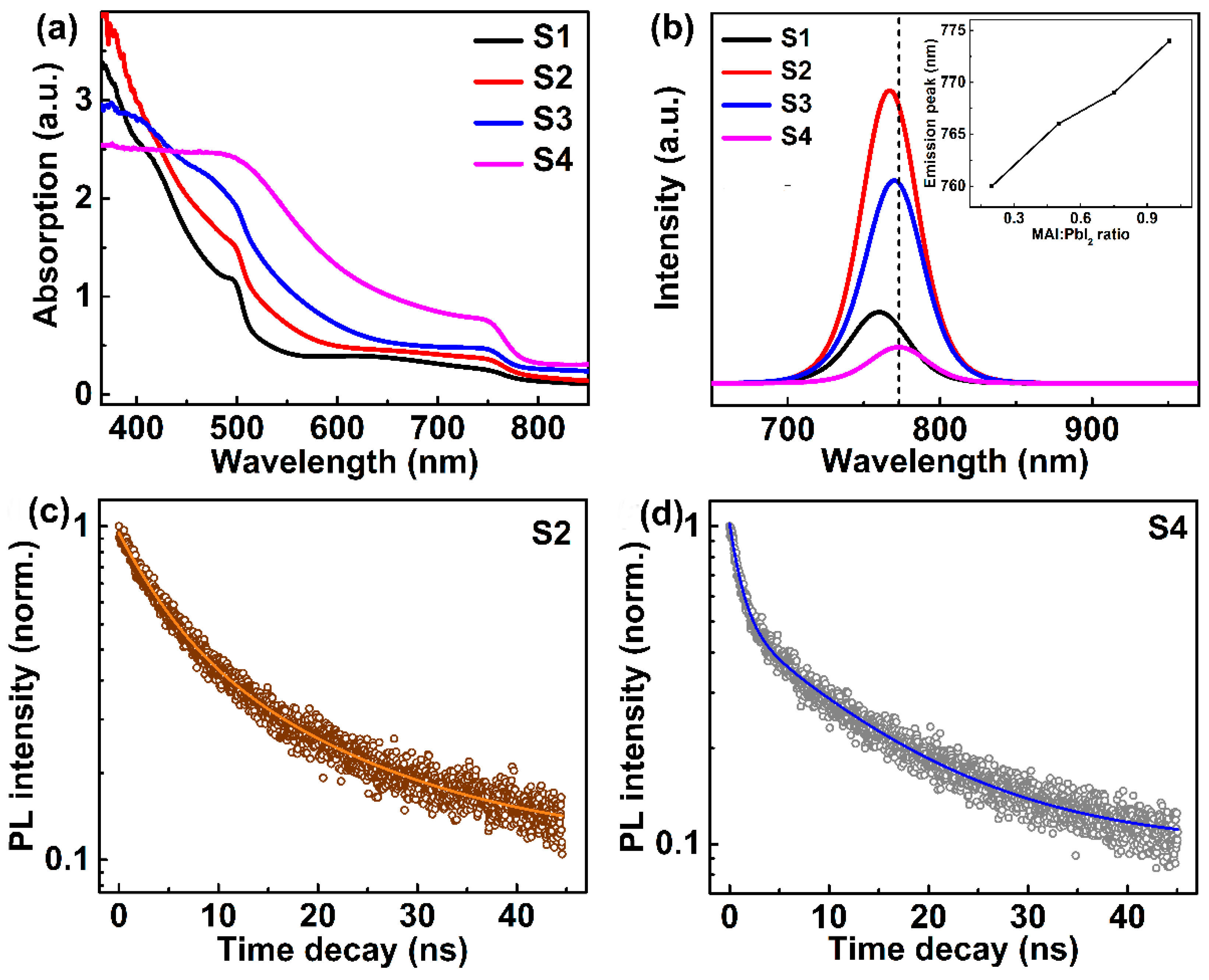
| Sample | A1 | τ1 (ns) | A2 | τ2 (ns) |
|---|---|---|---|---|
| S2 | 0.44 ± 0.03 (52%) | 4.42 ± 0.23 | 0.4 ± 0.03 (48%) | 16.3 ± 1.30 |
| S4 | 0.51 ± 0.01 (55%) | 1.16 ± 0.02 | 0.41 ± 0.01 (45%) | 13 ± 0.21 |
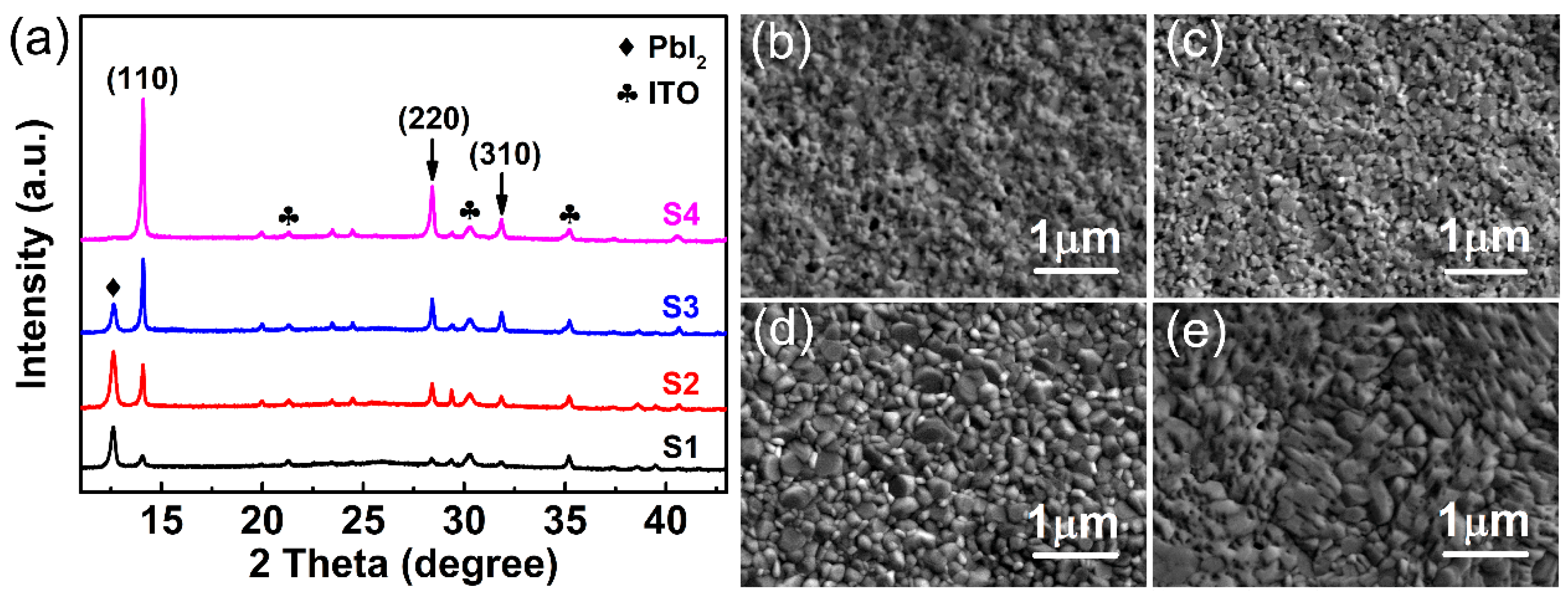
| Sample | S1 | S2 | S3 | S4 |
|---|---|---|---|---|
| Dark current (uA) | 1.787 × 10⁻³ | 6.018 × 10⁻³ | 1.254 × 10⁻² | 3.961 × 10⁻² |
| Photocurrent (uA) | 0.7993 | 4.083 | 2.352 | 2.161 |
| R (mA/W) | 13 | 64 | 37 | 34 |
| on/off ratio | 447 | 678 | 188 | 55 |
| tr (ms) | 1.25 | 0.86 | 2.3 | 31.9 |
| td (ms) | 1.6 | 1.5 | 10.3 | 385.8 |
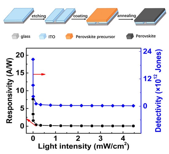
| Materials | R (A/W) | D* (Jones) | τr/τd (ms) | Light nm/(mW/cm2) | Bias (V) |
|---|---|---|---|---|---|
| MAPbI3/WS2 [11] | 17 | 2 × 10¹² | 2.7/7.5 | 505/0.0002 | 5 |
| MAPbI3 NWs [51] | 0.055 | 5 × 10¹⁰ | 150/53 | 532/40 | 0.1 |
| MAPbI3/TiO2 [52] | 0.49 × 10⁻⁶ | — | 20/20 | white/100 | 3 |
| MAPbI3/Rgo [53] | 0.074 | — | 40.9/28.8 | 520/3.2 | 5 |
| MAPbI3/NAYF4:Yb/Er [54] | 0.87 | 5.9 × 10¹² | 52/67 | 730/22.9 | 2 |
| MAPbI3 [55] | 8.95 | 2.9 × 10¹² | 7.7/6 | 532/0.37 | 10 |
| This work | 7.8 | 2.1 × 10¹³ | 0.86/1.5 | 405/0.005 | 5 |
© 2019 by the authors. Licensee MDPI, Basel, Switzerland. This article is an open access article distributed under the terms and conditions of the Creative Commons Attribution (CC BY) license (http://creativecommons.org/licenses/by/4.0/).
Share and Cite
Li, J.; Li, H.; Ding, D.; Li, Z.; Chen, F.; Wang, Y.; Liu, S.; Yao, H.; Liu, L.; Shi, Y. High-Performance Photoresistors Based on Perovskite Thin Film with a High PbI2 Doping Level. Nanomaterials 2019, 9, 505. https://doi.org/10.3390/nano9040505
Li J, Li H, Ding D, Li Z, Chen F, Wang Y, Liu S, Yao H, Liu L, Shi Y. High-Performance Photoresistors Based on Perovskite Thin Film with a High PbI2 Doping Level. Nanomaterials. 2019; 9(4):505. https://doi.org/10.3390/nano9040505
Chicago/Turabian StyleLi, Jieni, Henan Li, Dong Ding, Zibo Li, Fuming Chen, Ye Wang, Shiwei Liu, Huizhen Yao, Lai Liu, and Yumeng Shi. 2019. "High-Performance Photoresistors Based on Perovskite Thin Film with a High PbI2 Doping Level" Nanomaterials 9, no. 4: 505. https://doi.org/10.3390/nano9040505