

-
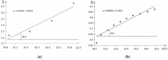
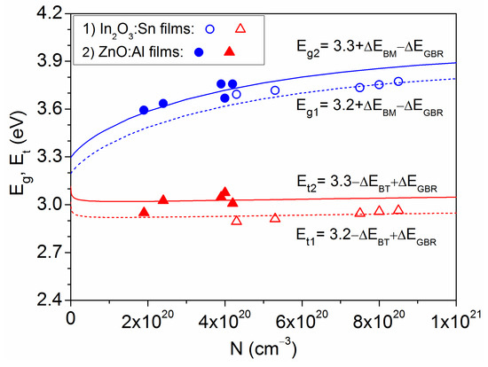
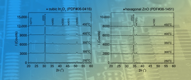
Lattice Distortion, Band Gap and Band Tail in Heavily Doped In2O3:Sn and ZnO:Al Thin Films Annealed at Different Temperatures in Nitrogen -
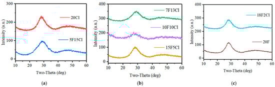
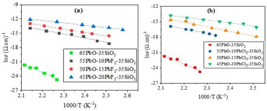
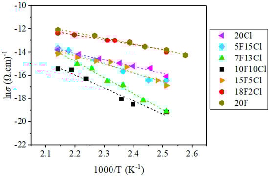
The Mixed Halogen-Ion Effect in Lead Silicate Glasses: A Correlative Study of Ionic Transport and Optical Spectroscopy in the 45PbO–xPbF2–(20−x)PbCl2–35SiO2 System
Journal Description
Electronic Materials
is an international, peer-reviewed, open access journal on fundamental science, engineering, and practical applications of electronic materials published quarterly online by MDPI.
- Open Access— free for readers, with article processing charges (APC) paid by authors or their institutions.
- High Visibility: indexed within Scopus, Ei Compendex, and other databases.
- Rapid Publication: manuscripts are peer-reviewed and a first decision is provided to authors approximately 21.7 days after submission; acceptance to publication is undertaken in 3.7 days (median values for papers published in this journal in the first half of 2026).
- Journal Rank: CiteScore - Q2 (Electrical and Electronic Engineering)
- Recognition of Reviewers: APC discount vouchers, optional signed peer review, and reviewer names published annually in the journal.
- Electronic Materials is a companion journal of Materials.
Latest Articles
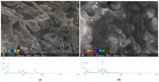
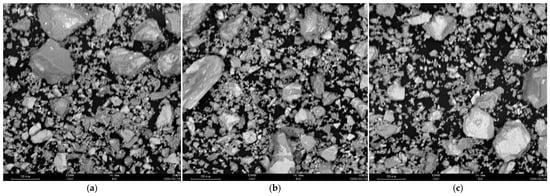
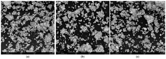
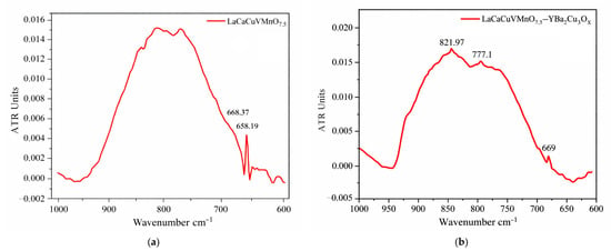
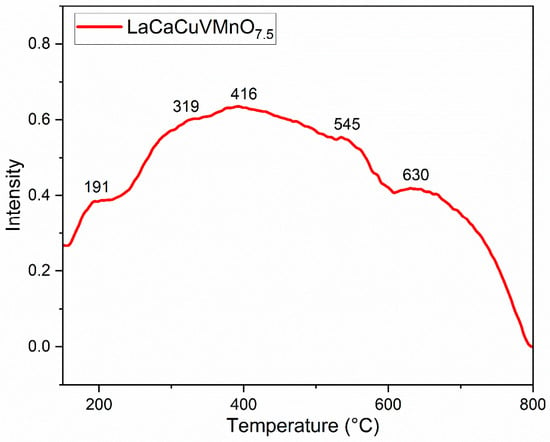
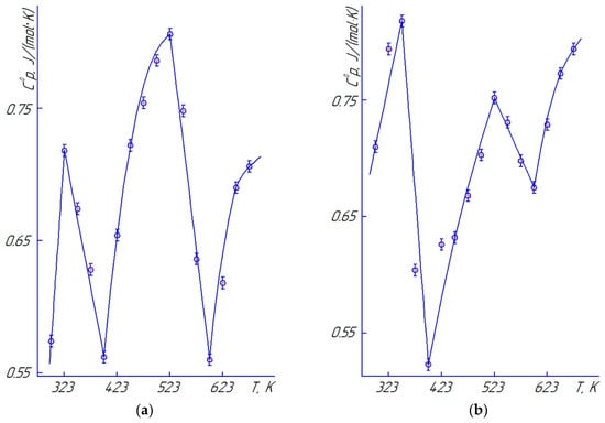
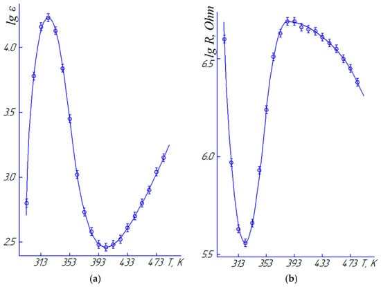
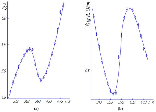
Structural and Functional Properties of the Oxide System LaCaCuVMnO7.5 and Its Composites with YBa2Cu3Ox
Electron. Mater. 2026, 7(3), 18; https://doi.org/10.3390/electronicmat7030018 - 6 Jul 2026
Abstract
►
Show Figures
Oxide systems with the nominal composition LaCaCuVMnO7.5 and composites modified with the YBa2Cu3Ox phase were synthesized by the solid-state reaction method. The phase composition and structural features were systematically investigated by X-ray diffraction (XRD), Rietveld refinement, and
[...] Read more.
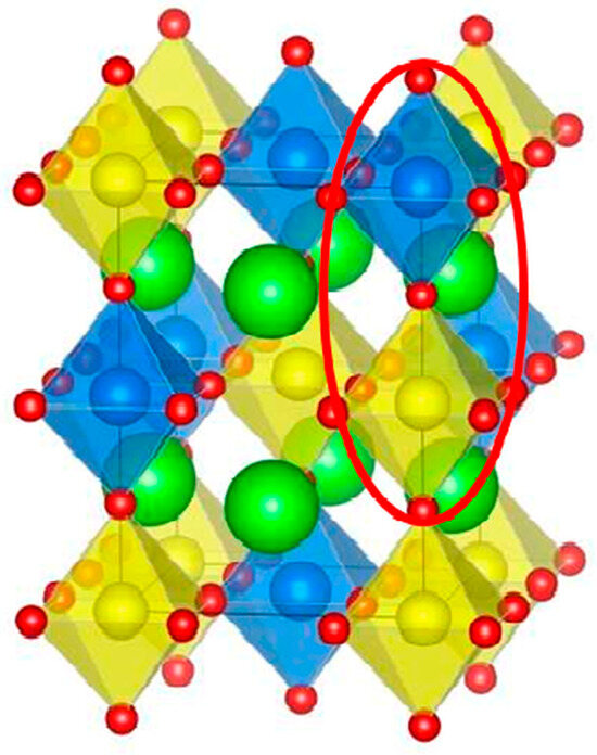
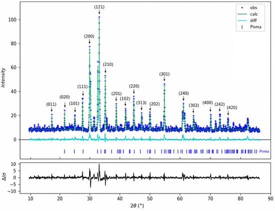
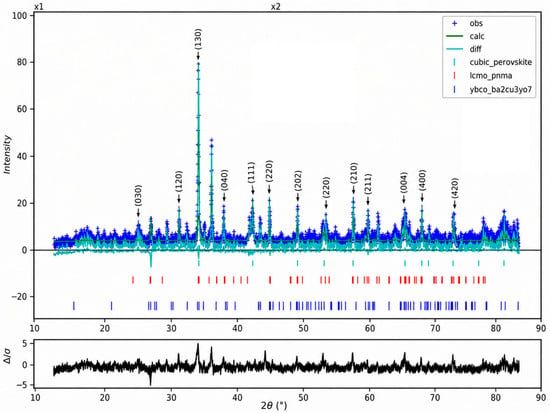
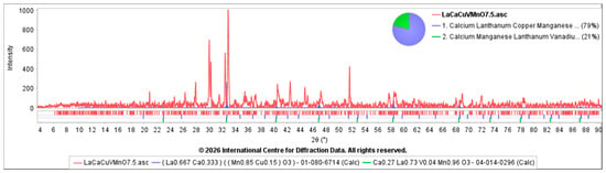
Oxide systems with the nominal composition LaCaCuVMnO7.5 and composites modified with the YBa2Cu3Ox phase were synthesized by the solid-state reaction method. The phase composition and structural features were systematically investigated by X-ray diffraction (XRD), Rietveld refinement, and scanning electron microscopy coupled with energy-dispersive X-ray spectroscopy (SEM–EDX). The parent oxide was found to form a two-phase system, consisting of an orthorhombic perovskite-like phase and a cubic manganite–vanadate phase, whereas the introduction of 10 wt.% YBa2Cu3Ox resulted in the formation of a three-phase composite containing an additional cuprate phase. Thermophysical investigations in the 298–673 K range revealed λ-type-like anomalies in the heat capacity, which may be associated with possible structural or interphase transformations in the investigated oxide systems. The incorporation of YBa2Cu3Ox significantly modified the temperature dependence of heat capacity and increased its values over both low- and high-temperature regions. Electrophysical measurements in the 293–483 K range confirmed the semiconducting nature of conductivity, while the addition of YBa2Cu3Ox reduced electrical resistance and enhanced dielectric permittivity. These findings demonstrate that YBa2Cu3Ox modification provides an effective route for tuning the thermophysical and electrophysical properties of LaCaCuVMnO7.5-based oxide systems, suggesting their potential as promising candidates for multifunctional oxide materials with possible electronic and sensor-related applications.
Full article
Open AccessArticle
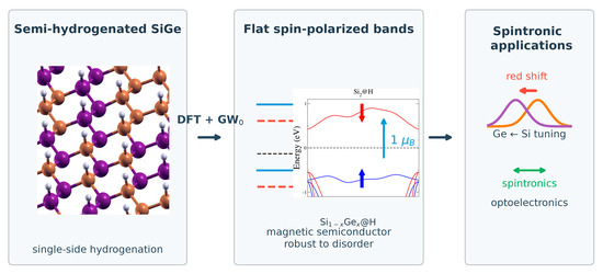
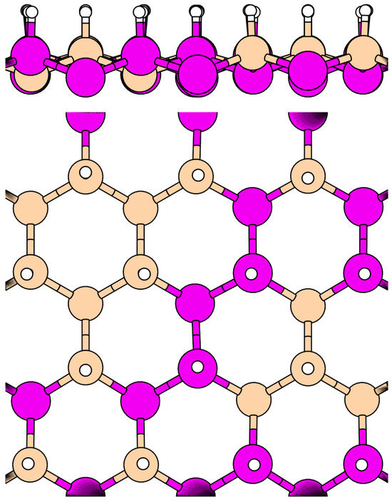
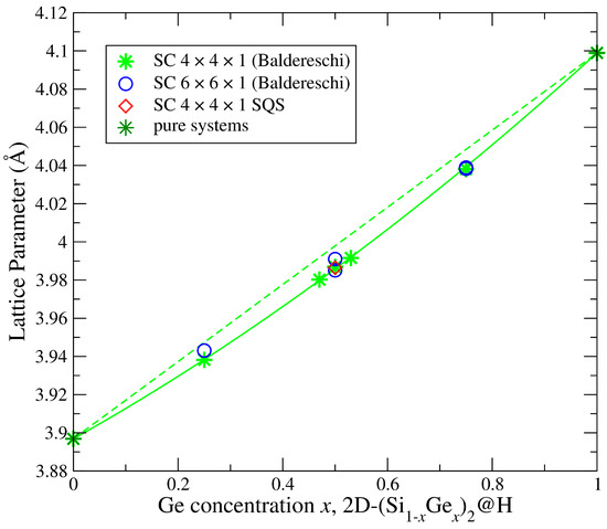
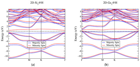
Emergence of a Magnetic Semiconducting Phase in Hydrogenated Two-Dimensional SiGe Random Alloys
by
Alberto Debernardi
Electron. Mater. 2026, 7(3), 17; https://doi.org/10.3390/electronicmat7030017 - 2 Jul 2026
Abstract
►▼
Show Figures
Two-dimensional (2D) group-IV materials are promising for spintronics due to their silicon compatibility and tunable properties. In this work, we investigate the structural, electronic, magnetic, and optical properties of semi-hydrogenated 2D SiGe random alloys—where hydrogen atoms saturate only one side of the atomic
[...] Read more.
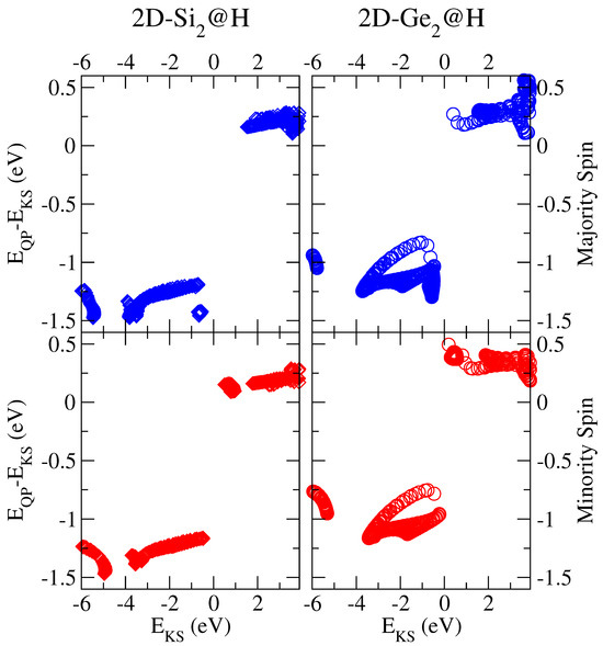
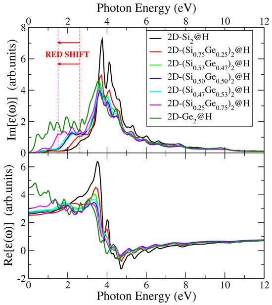
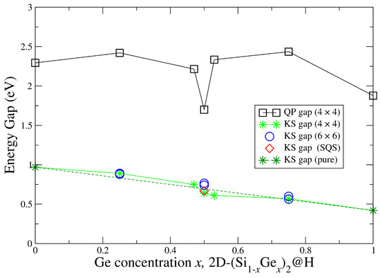
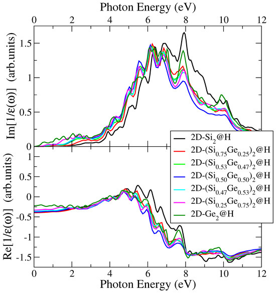
Two-dimensional (2D) group-IV materials are promising for spintronics due to their silicon compatibility and tunable properties. In this work, we investigate the structural, electronic, magnetic, and optical properties of semi-hydrogenated 2D SiGe random alloys—where hydrogen atoms saturate only one side of the atomic plane—using density functional theory and many-body perturbation theory ( ). Substitutional disorder is modeled via representative high-symmetry configurations introduced by Baldereschi and co-workers to enable quasiparticle and optical simulations in large supercells. We demonstrate that these semi-hydrogenated alloys possess an intrinsic magnetic semiconducting ground state, arising from the electronic structure of the system, with an integer magnetic moment of per primitive cell. The spin-resolved electronic structure features nearly flat frontier bands and a finite energy gap, which is significantly renormalized by quasiparticle corrections while maintaining robust spin polarization. These properties remain remarkably stable across different realizations of chemical disorder and over a wide range of alloy compositions considered in this work. Optical spectra calculated within the random phase approximation reveal a composition-dependent red-shift of the low-energy onset in the imaginary part of the dielectric function, consistent with the evolution of the quasiparticle electronic structure and the persistence of flat spin-polarized frontier bands. Our findings establish semi-hydrogenated 2D SiGe random alloys as a resilient model platform to explore interaction-driven magnetism in disordered two-dimensional systems, while simultaneously offering realistic prospects for spintronic and magneto-optoelectronic applications in the presence of chemical disorder.
Full article

Graphical abstract
Open AccessArticle
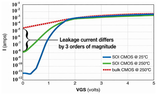
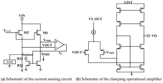
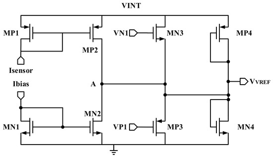
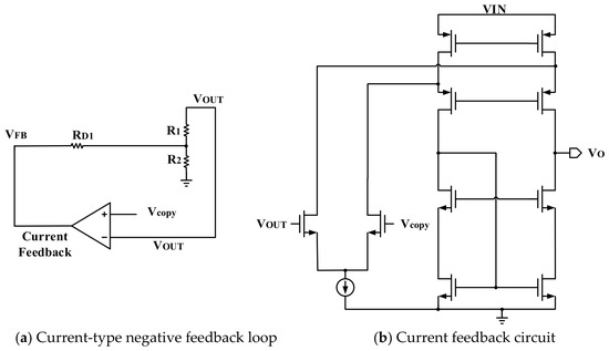
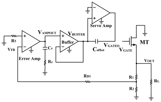
A Fast-Response LDO Based on High-Temperature 0.18 μm SOI Technology
by
Caiping Zheng, Muhammad Yasir Faheem, Qiaoying Gan, Sixian Li, Chengying Chen and Yufei Huang
Electron. Mater. 2026, 7(3), 16; https://doi.org/10.3390/electronicmat7030016 - 1 Jul 2026
Abstract
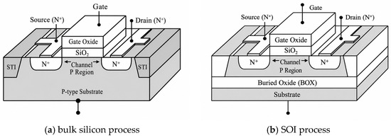
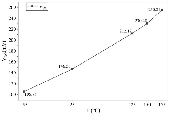
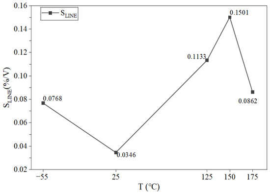
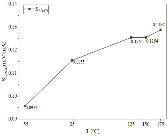
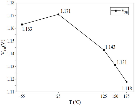
To meet the requirements of wide-temperature reliability and fast transient response in power management ICs for automotive, aerospace, and industrial applications, this paper presents a fast-response low-dropout regulator (LDO) based on a 0.18 μm high-temperature SOI process. Benefiting from the buried oxide isolation
[...] Read more.
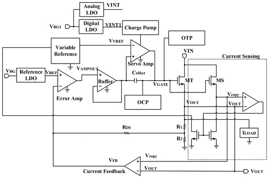
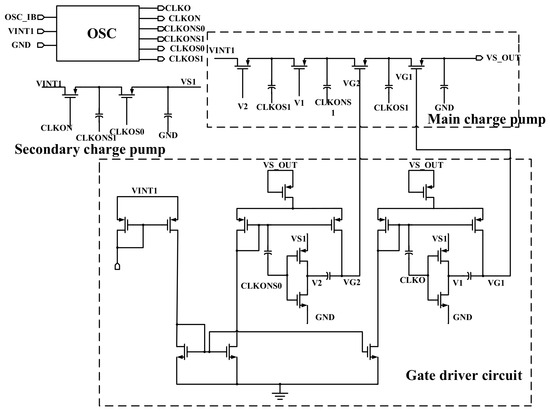
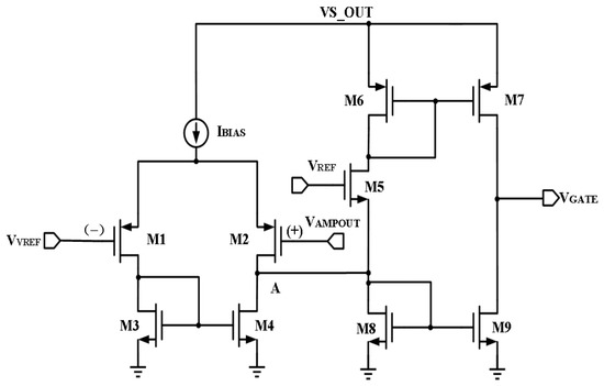
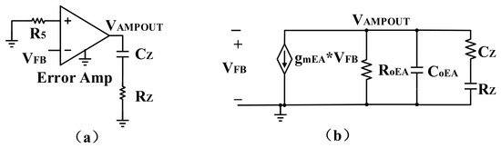
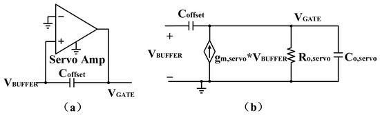
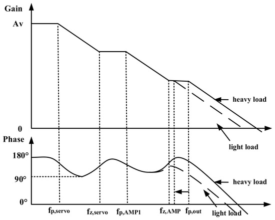
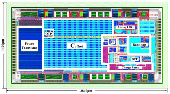
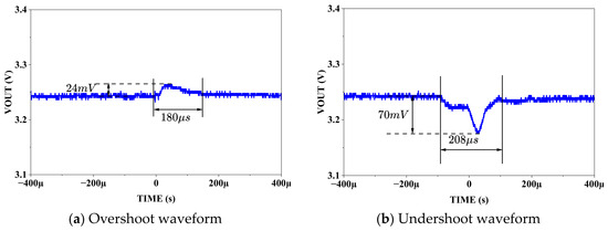
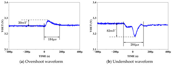
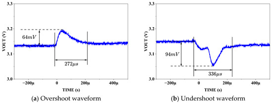
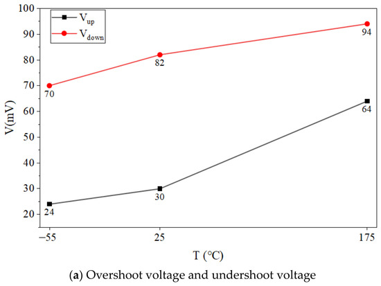
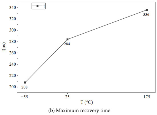
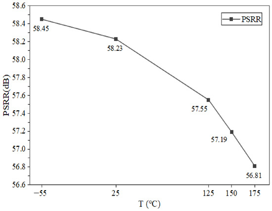
To meet the requirements of wide-temperature reliability and fast transient response in power management ICs for automotive, aerospace, and industrial applications, this paper presents a fast-response low-dropout regulator (LDO) based on a 0.18 μm high-temperature SOI process. Benefiting from the buried oxide isolation structure of the SOI technology, leakage current and parasitic effects under high-temperature conditions are effectively suppressed. The proposed LDO employs an NMOS power transistor, with an on-chip charge pump used to enhance the gate driving capability. In addition, a triple-loop regulation scheme consisting of a main negative feedback loop, an auxiliary positive feedback loop, and a current-mode feedback loop is adopted to improve transient performance and enhance loop stability. The fabricated chip occupies an area of 2840 μm × 1490 μm and supports an input voltage range of 3–5.5 V and an output voltage range of 1.2–3.3 V. Over a temperature range of −55 °C to 175 °C, the LDO can deliver a maximum load current of 400 mA. At 175 °C, the measured overshoot and undershoot voltages are 64 mV and 94 mV, respectively, with a maximum recovery time of 336 μs. Moreover, the power supply rejection ratio (PSRR) reaches 56.8 dB at 100 Hz. Experimental results demonstrate that the proposed LDO exhibits excellent high-temperature adaptability, strong load-driving capability, and superior transient response performance.
Full article
(This article belongs to the Special Issue Emerging Trends in Electronic Materials and Functional Nanostructures)
►▼
Show Figures

Figure 1
Open AccessArticle
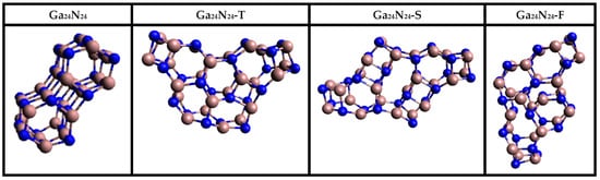
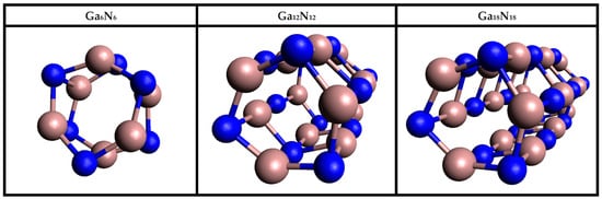
Structural Evolution and Optoelectronic Properties of GaxNx Nanostructures: From Cubic to Hexagonal Configurations
by
Christina Papaspiropoulou, Fotios I. Michos and Michail M. Sigalas
Electron. Mater. 2026, 7(3), 15; https://doi.org/10.3390/electronicmat7030015 - 1 Jul 2026
Abstract
►▼
Show Figures
In this work, the structural, electronic, optical, and vibrational properties of gallium nitride (GaxNx) nanostructures were systematically investigated using density functional theory (DFT) and time-dependent DFT (TD-DFT). A series of nanoparticles was constructed starting from a cubic-like Ga4
[...] Read more.
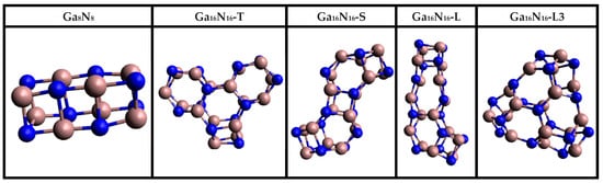
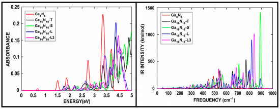
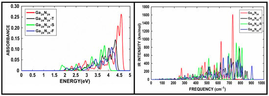
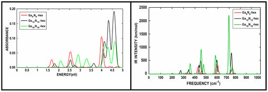
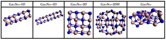
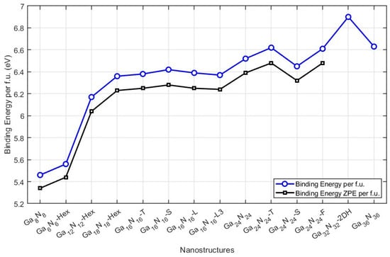
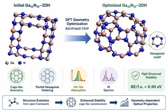
In this work, the structural, electronic, optical, and vibrational properties of gallium nitride (GaxNx) nanostructures were systematically investigated using density functional theory (DFT) and time-dependent DFT (TD-DFT). A series of nanoparticles was constructed starting from a cubic-like Ga4N4 building unit, leading to one-dimensional (1D), two-dimensional (2D), three-dimensional (3D), and hexagonal configurations. Geometry optimizations and vibrational frequency calculations were performed at the B3LYP/def2-TZVP level, while optical properties were investigated using TD-DFT with the CAM-B3LYP functional. Only dynamically stable structures without imaginary vibrational frequencies were considered for spectroscopic analysis. The results reveal a strong dependence of the optical and vibrational behavior on nanoparticle size and geometry. Larger and lower-symmetry systems exhibit broader and red-shifted UV–Vis absorption spectra together with richer IR vibrational features. In contrast, elongated low-dimensional configurations such as Ga12N12–1D and Ga16N16–1D/2D were found to be dynamically unstable. The investigated nanostructures also show a clear tendency toward structural reorganization from cubic-like motifs to compact hexagonal arrangements related to the wurtzite phase of bulk GaN. Benchmark analysis demonstrates that CAM-B3LYP provides reliable excitation energies at moderate computational cost. Overall, the obtained results highlight the strong coupling between structure and optoelectronic properties in GaxNx nanostructures and indicate their potential for nanoscale optoelectronic and photonic applications.
Full article

Graphical abstract
Open AccessArticle
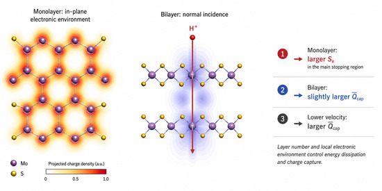
Monolayer and Bilayer MoS2 Under Proton Irradiation: Electronic Stopping and Charge Capture Revealed by Real-Time TDDFT
by
Ligang Wang, Guanxiang Yang, Lihongye Liao and Qiang Zhao
Electron. Mater. 2026, 7(2), 14; https://doi.org/10.3390/electronicmat7020014 - 18 Jun 2026
Abstract
Monolayer and few-layer MoS2 are promising two-dimensional electronic materials, but proton irradiation can trigger ultrafast electronic excitation and charge transfer before defect formation. Here, real-time time-dependent density functional theory (RT-TDDFT) is used to investigate proton-induced electronic stopping and localized charge capture in
[...] Read more.
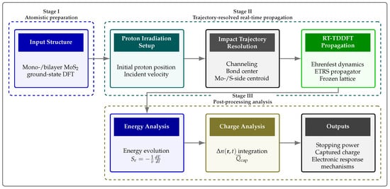
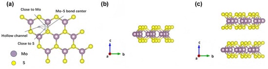
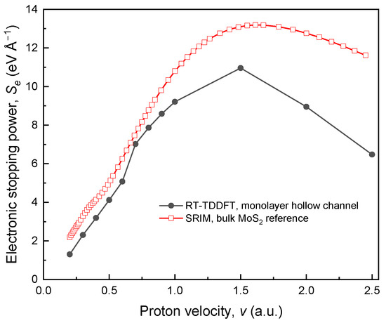
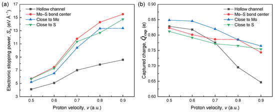
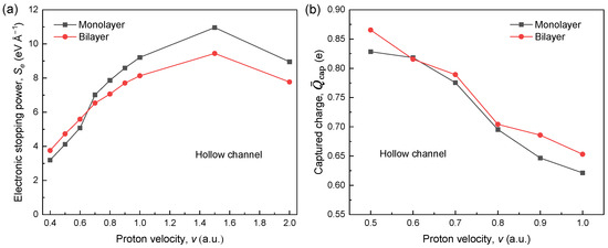
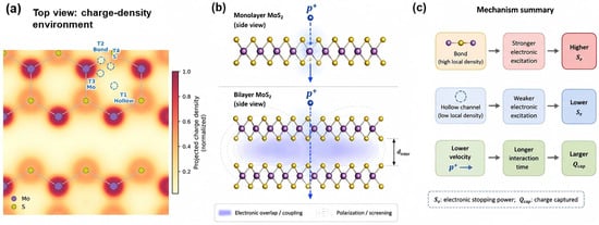
Monolayer and few-layer MoS2 are promising two-dimensional electronic materials, but proton irradiation can trigger ultrafast electronic excitation and charge transfer before defect formation. Here, real-time time-dependent density functional theory (RT-TDDFT) is used to investigate proton-induced electronic stopping and localized charge capture in monolayer and bilayer MoS2 under normal incidence. Four impact positions are examined in monolayer MoS2, namely, the hollow channel, the Mo–S bond center, and two trajectories close to Mo and S atoms. Under hollow channel incidence, the stopping power shows a non-monotonic dependence on proton velocity. When comparing the different trajectories, the hollow channel path gives the lowest stopping power, whereas the Mo–S bond center path gives the highest values, indicating strong sensitivity to the in-plane valence charge distribution. By contrast, the time-averaged localized captured charge decreases with increasing velocity and is generally largest for the close to Mo trajectory. Under the same hollow channel condition, the monolayer stopping power exceeds the bilayer value in the main stopping region, whereas the bilayer generally shows slightly enhanced localized charge capture. These results show that electronic stopping and localized charge capture are distinct but coupled microscopic components of proton-induced electronic response in MoS2 and provide first-principles insight relevant to ion-beam processing and radiation-tolerant two-dimensional devices.
Full article
(This article belongs to the Special Issue Emerging Trends in Electronic Materials and Functional Nanostructures)
►▼
Show Figures

Graphical abstract
Open AccessArticle
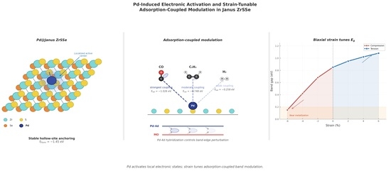
Pd-Induced Electronic Activation and Strain-Tunable Adsorption-Coupled Electronic Modulation in Janus ZrSSe Monolayers
by
Guanxiang Yang, Ligang Wang, Lihongye Liao, Qiang Zhao and Xiaoping Ouyang
Electron. Mater. 2026, 7(2), 13; https://doi.org/10.3390/electronicmat7020013 - 8 Jun 2026
Abstract
►▼
Show Figures
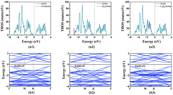
Pd-decorated Janus ZrSSe monolayers provide a promising platform for adsorption-coupled electronic modulation in two-dimensional materials. Using first-principles density functional theory, we systematically investigate the structural stability, electronic properties, and adsorbate-induced electronic response of Pd-modified Janus ZrSSe. The results show that Pd is most
[...] Read more.
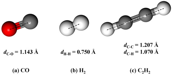
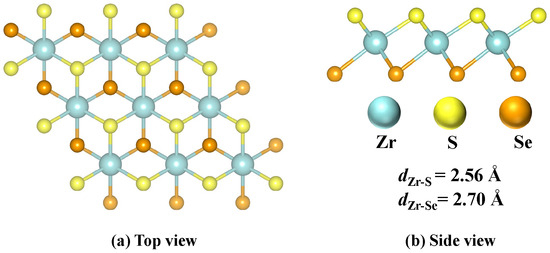
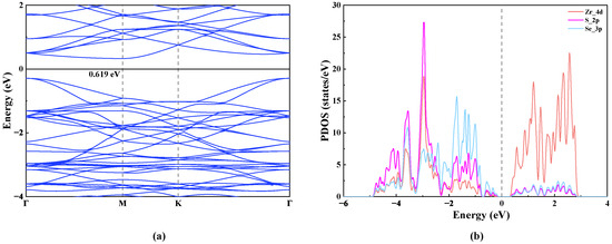
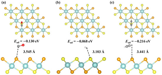
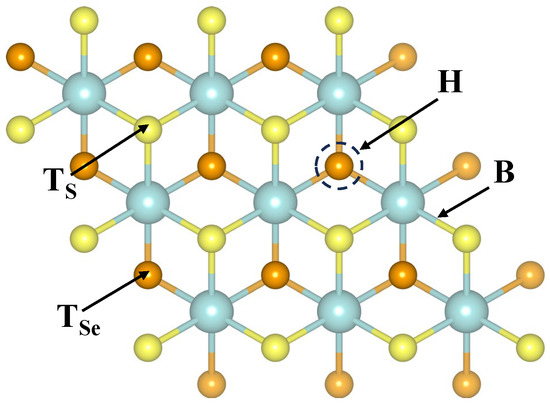
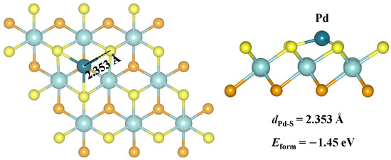
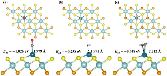
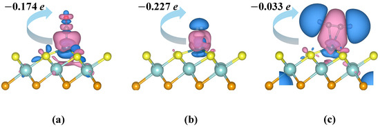
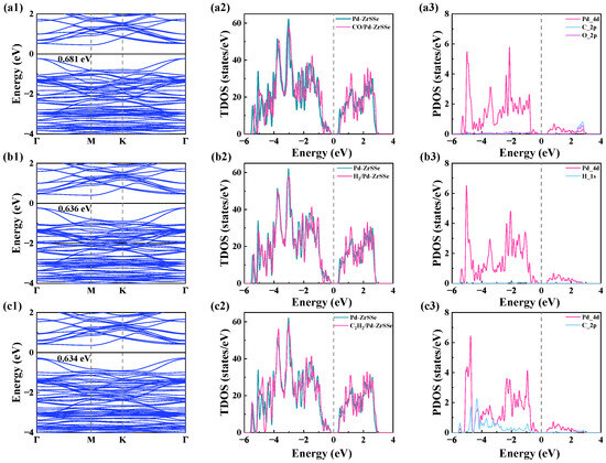
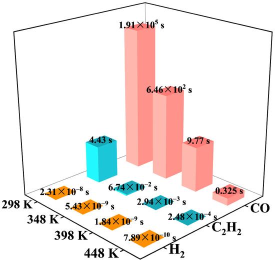
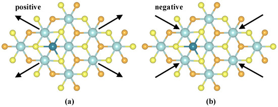
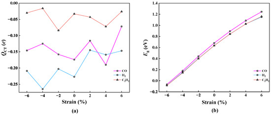
Pd-decorated Janus ZrSSe monolayers provide a promising platform for adsorption-coupled electronic modulation in two-dimensional materials. Using first-principles density functional theory, we systematically investigate the structural stability, electronic properties, and adsorbate-induced electronic response of Pd-modified Janus ZrSSe. The results show that Pd is most stably anchored at the hollow site on the S-terminated surface, with a formation energy of eV, while substitutional incorporation remains energetically unfavorable even after HSE06 refinement. Compared with pristine ZrSSe, Pd decoration markedly strengthens the interaction with adsorbates, leading to strong chemisorption for CO ( eV) and C2H2 ( eV), whereas H2 remains comparatively weakly bound ( eV). Electronic-structure analysis reveals that CO induces the most pronounced perturbation because of strong orbital hybridization between Pd 4d states and C/O 2p states, resulting in the largest band-edge modulation among the three adsorbates. More importantly, biaxial strain provides an effective external degree of freedom for continuously tuning the electronic structure: tensile strain widens the band gap, whereas compressive strain systematically narrows it and ultimately drives a semiconductor-to-metal transition at sufficiently large compression. These findings establish Pd-decorated Janus ZrSSe as a strain-tunable electronic material in which adsorption, orbital hybridization, and band-edge evolution are intimately coupled, offering fundamental insights into controllable electronic modulation in polar two-dimensional systems.
Full article

Graphical abstract
Open AccessArticle
Amorphous GaOx Thin Film-Based Optoelectronic Artificial Synapses Towards Physical Reservoir Computing
by
Kotaro Takanashi, Manami Miyazaki, Iori Yamasaki, Hiroaki Komatsu, Toshiya Kounoue, Masatoshi Koyama and Takashi Ikuno
Electron. Mater. 2026, 7(2), 12; https://doi.org/10.3390/electronicmat7020012 - 6 Jun 2026
Abstract
►▼
Show Figures
This study investigated the optoelectronic synaptic properties of amorphous gallium oxide (GaOx) thin films for low-power physical reservoir computing (PRC) applications. The fabricated devices were irradiated with time series UV-C light to characterize the paired pulse facilitation (PPF) index, a fundamental
[...] Read more.
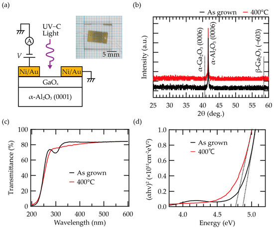
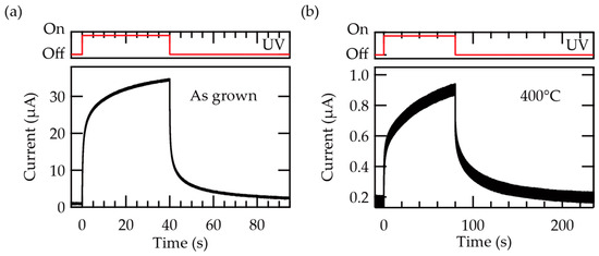
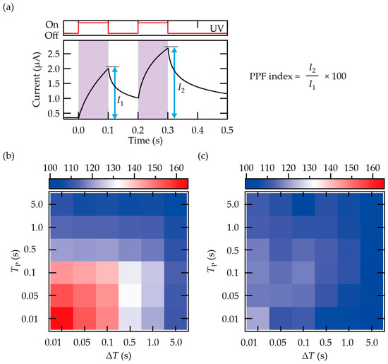
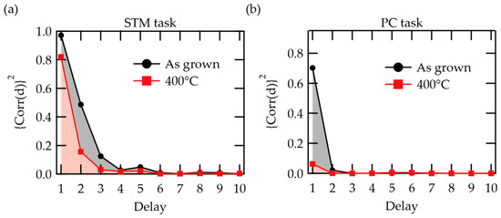
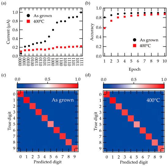
This study investigated the optoelectronic synaptic properties of amorphous gallium oxide (GaOx) thin films for low-power physical reservoir computing (PRC) applications. The fabricated devices were irradiated with time series UV-C light to characterize the paired pulse facilitation (PPF) index, a fundamental synaptic property governed by transient photocurrent dynamics. Furthermore, the short-term memory (STM) capacity and parity check (PC) nonlinearity were quantitatively evaluated as essential PRC performance metrics, alongside a practical demonstration using a handwritten digit recognition task. The experimental results revealed a high PPF index when the width and interval of the input light pulses were comparable to or shorter than the inherent photocurrent time constants of the device. Although the evaluated nonlinearity was lower than that of conventional optoelectronic artificial synapses based on other semiconductor materials, the GaOx device exhibited a comparable short-term memory capacity. Consequently, the reservoir layer achieved a high classification accuracy of approximately 90% in the handwritten digit recognition task. As these performance metrics were higher than those of the annealed sample, the device without annealing proved to be more suitable for PRC applications. These findings indicate that the amorphous GaOx thin film device holds significant potential to serve as a robust, UV-C-responsive edge artificial intelligence (AI) sensor in harsh environments, such as outer space.
Full article

Figure 1
Open AccessArticle
In Situ Coating Thickness Measurement of Parylene Using a Capacitive Sensor
by
Manuel Seidenath, Daniel Jäger, Jochen Wilhelm, Hubert Rauh and Martin Maerz
Electron. Mater. 2026, 7(2), 11; https://doi.org/10.3390/electronicmat7020011 - 2 Jun 2026
Abstract
►▼
Show Figures
With parylene coatings, conventional layer thickness measurement methods such as gravimetry, reflectometry, and cross-sectional microscopy are performed post-process and do not allow real-time monitoring or control. This paper presents a novel in situ measurement method based on the capacitance change in interdigitated copper
[...] Read more.
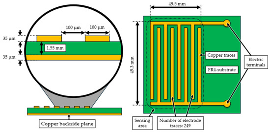
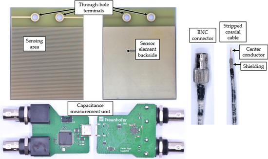
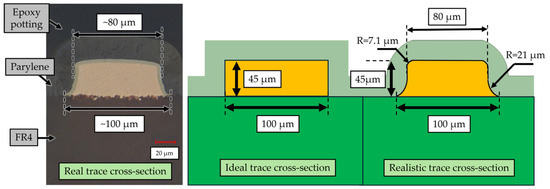
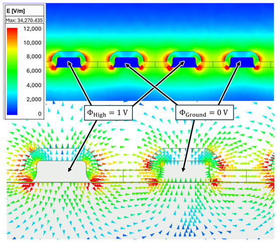
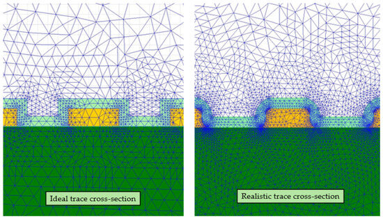
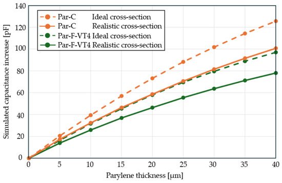
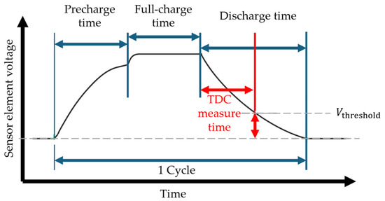
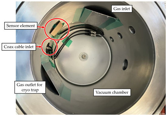
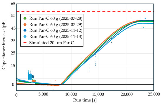
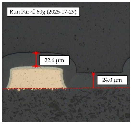
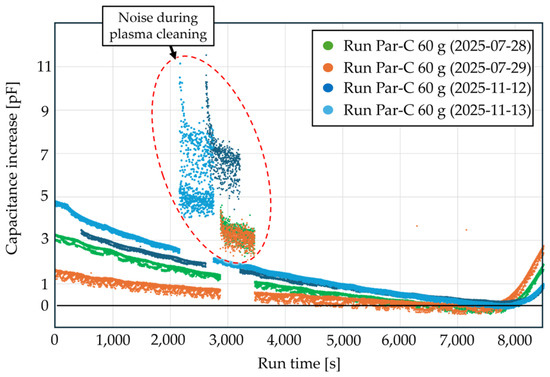
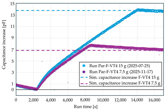
With parylene coatings, conventional layer thickness measurement methods such as gravimetry, reflectometry, and cross-sectional microscopy are performed post-process and do not allow real-time monitoring or control. This paper presents a novel in situ measurement method based on the capacitance change in interdigitated copper electrodes fabricated on a printed circuit board (PCB). As parylene deposits on this sensor, the effective permittivity above the electrodes increases from (vacuum) to (parylene), causing a measurable capacitance change. Finite element simulations were performed to model the relationship between layer thickness and sensor capacitance. Experimental validation with parylene C and F-VT4 demonstrated good agreement between simulation and measurement. Four consecutive parylene C runs with 60 g raw material showed reproducible capacitance increases of 49–53 pF, corresponding to layer thicknesses of 20–25 µm, verified by cross-sectional microscopy. Two coating runs were performed with parylene F-VT4 with target layer thicknesses of 2.5 µm and 5 µm. They show particularly good agreement with the simulation. The proposed method enables real-time process monitoring and provides a foundation for closed-loop control of parylene CVD processes.
Full article

Figure 1
Open AccessArticle
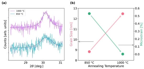
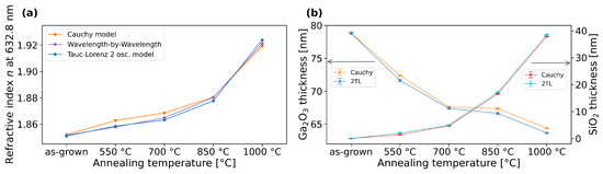
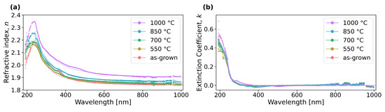
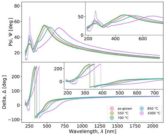
Study on the Effect of Annealing on Ga2O3 Thin Films Deposited on Silicon by RF Sputtering
by
Ana Sofia Sousa, Duarte M. Esteves, Tiago T. Robalo, Mário S. Rodrigues, Katharina Lorenz and Marco Peres
Electron. Mater. 2026, 7(2), 10; https://doi.org/10.3390/electronicmat7020010 - 26 May 2026
Abstract
►▼
Show Figures
Gallium oxide is an ultra-wide bandgap semiconductor with excellent opto-electronic properties, making it a highly promising material for a wide range of applications and devices. In this article, we report how the optical, morphological, structural, and compositional properties of -Ga2O
[...] Read more.
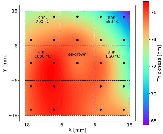
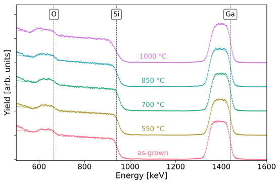
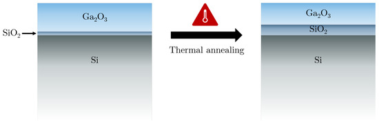
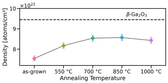
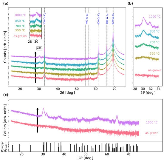
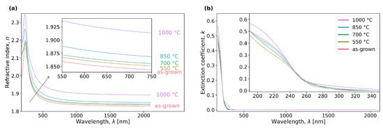
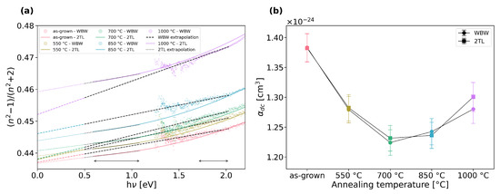
Gallium oxide is an ultra-wide bandgap semiconductor with excellent opto-electronic properties, making it a highly promising material for a wide range of applications and devices. In this article, we report how the optical, morphological, structural, and compositional properties of -Ga2O3 thin films deposited by RF Sputtering on silicon substrates are affected by thermal treatments. Ellipsometric spectra recorded at multiple angles of incidence from several samples subjected to thermal annealing in the range of 550–1000 °C were analyzed to extract the optical functions using appropriate multilayer models. This analysis is complemented by compositional, structural, and morphological characterization techniques. We observed two main stages of crystallization with increasing annealing temperature; up to 700 °C, there is an increase in density and then, for 700–1000 °C, there is an improvement in crystallinity. While the refractive index increases continuously throughout this process, we found that the polarizability of the samples decreases in the first stage and increases in the second. These observations demonstrate that thermal treatments are a powerful tool to tune the optical properties of Ga2O3 thin films for device applications.
Full article

Figure 1
Open AccessCommunication
Room-Temperature Operation of an Injection-Type Ballistic Rectifier on Bilayer Graphene
by
Ihor Petrov and Ulrich Kunze
Electron. Mater. 2026, 7(2), 9; https://doi.org/10.3390/electronicmat7020009 - 8 May 2026
Abstract
►▼
Show Figures
This work investigates the performance improvement of a four-probe ballistic rectifier on bilayer graphene (BLG) through the formation of an energy gap under a perpendicular electric field. For this purpose, exfoliated BLG was deposited on oxidized n+-Si and structured into an
[...] Read more.
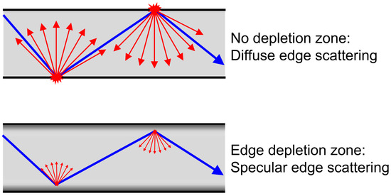
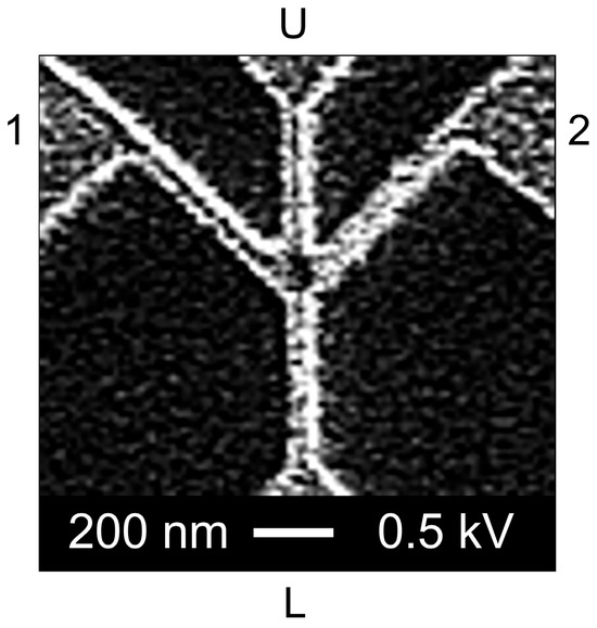
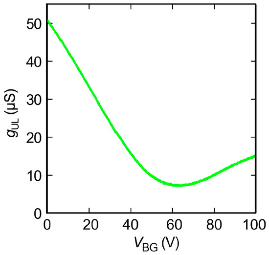
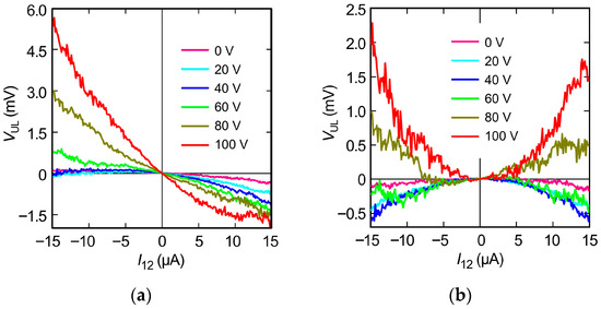
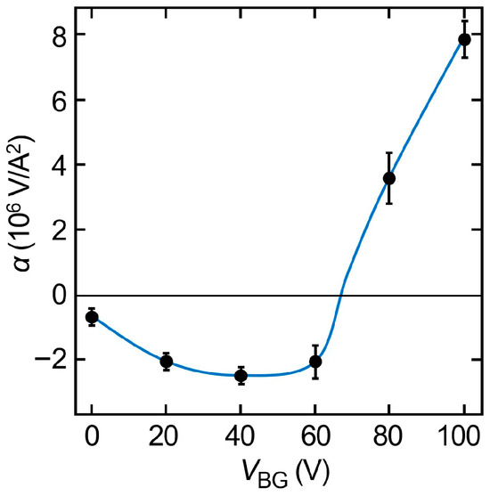
This work investigates the performance improvement of a four-probe ballistic rectifier on bilayer graphene (BLG) through the formation of an energy gap under a perpendicular electric field. For this purpose, exfoliated BLG was deposited on oxidized n+-Si and structured into an asymmetric cross junction with 90 nm wide channels. The junction consists of a straight voltage stem (contacts U, L) and slanted current injectors (contacts 1, 2). The differential conductance of the stem, gUL, as a function of back-gate bias, VBG, reveals clear indications of energy gap formation and lateral depletion zones at the edges of the channel. The DC characteristic of the ballistic rectifier, VUL(I12), shows an increase in the output voltage VUL with increasing VBG. We attribute this to reduced diffuse scattering at the rough edges when the lateral depletion zones form smooth barriers.
Full article

Graphical abstract
Open AccessReview
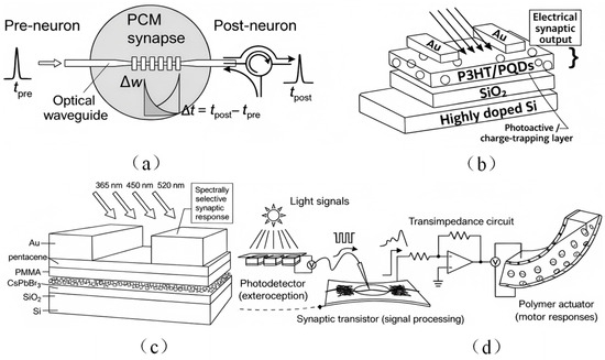
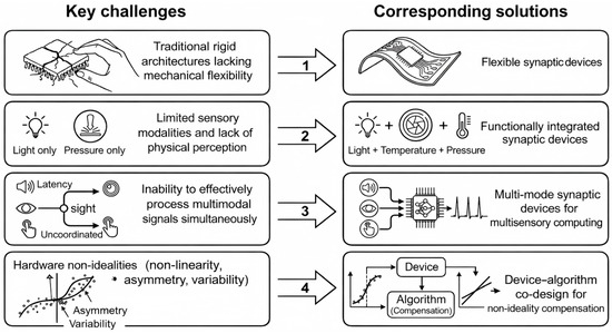
Tactile and Visual Artificial Synaptic Devices: Progress and Challenges
by
Zhifeng Chen, Chengying Chen and Yufei Huang
Electron. Mater. 2026, 7(2), 8; https://doi.org/10.3390/electronicmat7020008 - 15 Apr 2026
Abstract
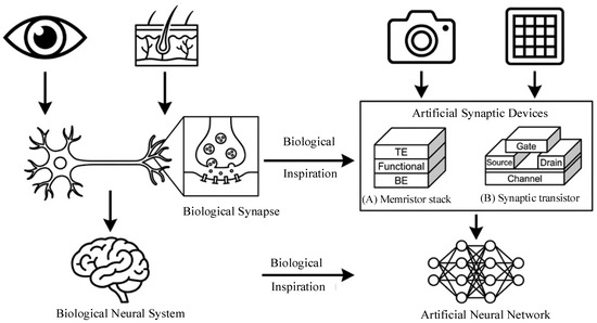
The von Neumann architecture faces a “memory wall” problem due to the physical separation of memory and processor, posing major challenges to energy efficiency and latency in the era of artificial intelligence. To overcome these bottlenecks, artificial synaptic devices inspired by biological systems
[...] Read more.
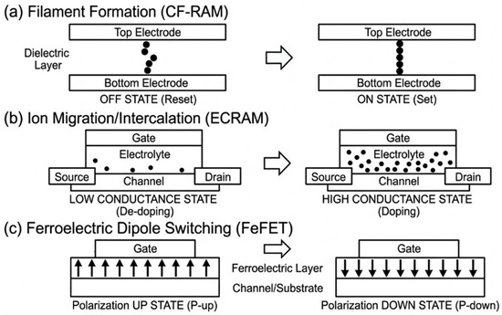
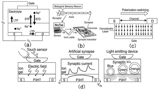
The von Neumann architecture faces a “memory wall” problem due to the physical separation of memory and processor, posing major challenges to energy efficiency and latency in the era of artificial intelligence. To overcome these bottlenecks, artificial synaptic devices inspired by biological systems have emerged as an important research direction. By integrating sensing and computing functions at the device level, these architectures provide a promising approach for the efficient processing of natural physical signals. Supported by advances in functional materials and artificial neural network (ANN) algorithms, artificial synaptic devices are capable of perceiving and processing various external stimuli, showing strong potential for applications in intelligent electronic skins, robotics, and edge computing. This review provides a comprehensive overview of recent advances in artificial synaptic devices, with particular emphasis on tactile and visual sensing applications. We discuss representative device types and operating mechanisms, analyze critical challenges from the perspectives of material engineering and functional integration, and further summarize potential solutions and future trends toward multimodal sensory–memory–computing systems.
Full article
(This article belongs to the Special Issue Emerging Trends in Electronic Materials and Functional Nanostructures)
►▼
Show Figures

Figure 1
Open AccessArticle
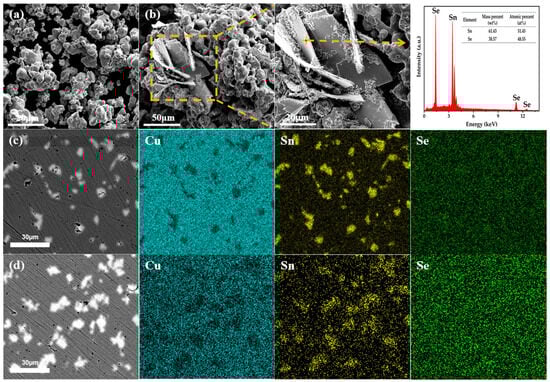
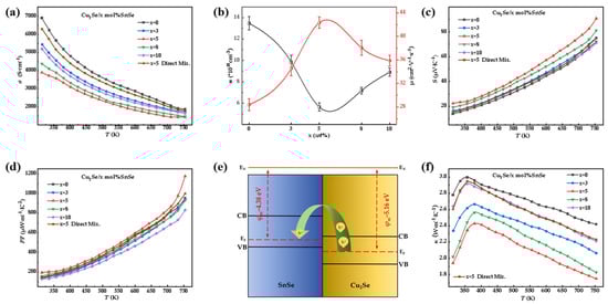
In Situ Compositing-Induced Matrix Planarization for Enhanced Thermoelectric Properties of β-Cu2Se/SnSe Composites
by
Zhonghe Zhu, Changcun Li, Haibo Wang, Yvcui Sun, Jing Qiao, Mingqian Hao, Wei Zhao and Degang Zhao
Electron. Mater. 2026, 7(2), 7; https://doi.org/10.3390/electronicmat7020007 - 9 Apr 2026
Abstract
►▼
Show Figures
With the intensification of the energy crisis and environmental issues, thermoelectric conversion technology has become a research focus due to its ability to directly convert thermal and electrical energy. β-Cu2Se thermoelectric materials have garnered considerable attention owing to their distinctive physical
[...] Read more.
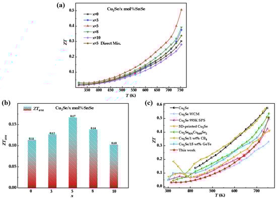
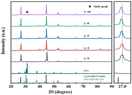
With the intensification of the energy crisis and environmental issues, thermoelectric conversion technology has become a research focus due to its ability to directly convert thermal and electrical energy. β-Cu2Se thermoelectric materials have garnered considerable attention owing to their distinctive physical and chemical characteristics. However, their practical implementation is hindered by the inherent imbalance between electrical and thermal transport properties. In this work, β-Cu2Se/SnSe composite thermoelectric materials were successfully synthesized via a facile and scalable in situ compositing strategy by introducing SnSe micro-flakes as the secondary phase. The results demonstrate that the introduced SnSe secondary phase effectively modulates the carrier concentration and enhances the density-of-states effective mass through the energy filtering effect and resonant energy level regulation, thereby significantly optimizing the electrical transport properties. Meanwhile, the abundant heterointerfaces formed between the β-Cu2Se matrix and introduced SnSe secondary phase induce intense phonon scattering, which efficiently suppresses the lattice thermal conductivity of the β-Cu2Se/SnSe composites. Benefiting from the synergistic optimization of electrical and thermal transport behaviors, the β-Cu2Se/5 mol% SnSe composite sample achieves a maximum figure of merit (ZT) value of ~0.51 at 750 K, which represents a 70% enhancement compared with the pristine β-Cu2Se and a 60% improvement compared with the direct composite sample. This study provides a simple and effective in situ composite strategy for designing and synthesizing high-performance thermoelectric materials.
Full article

Figure 1
Open AccessReview
Additive Manufacturing Technologies for Electronic Integration and Packaging
by
Arashdeep Singh and Ahsan Mian
Electron. Mater. 2026, 7(1), 6; https://doi.org/10.3390/electronicmat7010006 - 4 Mar 2026
Cited by 1
Abstract
►▼
Show Figures
Additive Manufacturing (AM) and printing-based fabrication technologies have emerged as powerful enablers for next-generation electronic integration and packaging, addressing the growing limitations of conventional subtractive manufacturing techniques. As electronic systems continue to scale toward higher operating frequencies (10–110 GHz and beyond) and increased
[...] Read more.
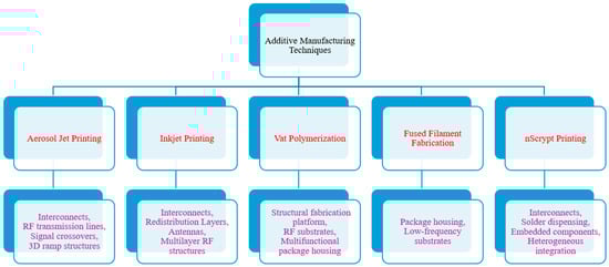
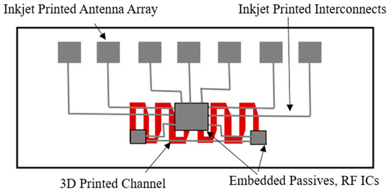
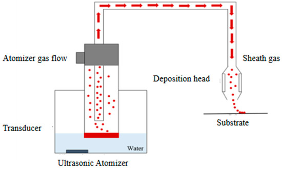
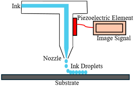
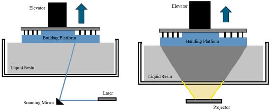
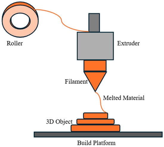
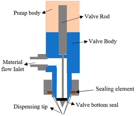
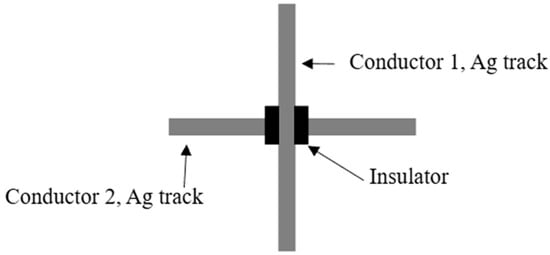
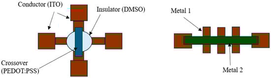
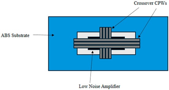
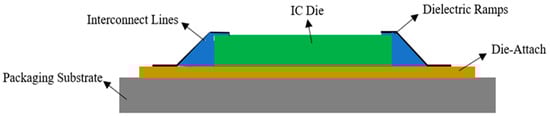
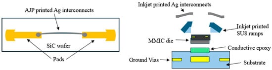
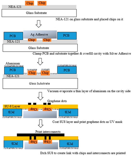
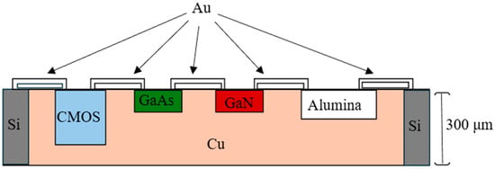
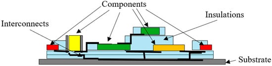
Additive Manufacturing (AM) and printing-based fabrication technologies have emerged as powerful enablers for next-generation electronic integration and packaging, addressing the growing limitations of conventional subtractive manufacturing techniques. As electronic systems continue to scale toward higher operating frequencies (10–110 GHz and beyond) and increased functional density (>104 interconnects/cm2), traditional packaging approaches struggle with rigid design constraints, complex processing steps (>15–25 fabrication steps), high tooling costs ($10,000–$100,000 for mask and molds) and limited compatibility with heterogeneous integration. In this review, a comprehensive and critical overview of major additive manufacturing and printing technologies including aerosol jet printing, inkjet printing, vat polymerization, fused filament fabrication (FFF) and nScrypt printing is presented from the perspective of electronic assembly and packaging. The fundamental working mechanisms, material compatibility, resolution limits, scalability, and reliability considerations of each technique are systematically discussed. From a manufacturing standpoint, AM reduces material waste by 50–90% compared to subtractive PCB processing and eliminates tooling costs, enabling low-volume prototyping with per-unit fabrication costs reduced by 30–70% for small batches (<100 units). Production throughput varies widely, from 1 to 20 cm2/min for high-resolution direct write systems to >100 cm2/min for scalable inkjet systems. Moreover, it is discussed how these technologies enable advanced packaging architectures such as printed signal crossovers, three-dimensional interconnects, ramps, and embedded chip assemblies. Recent research efforts and reported demonstrations are analyzed to highlight the advantages and current limitations of additive manufacturing for high-frequency, RF, and system-on-package (SoP) applications. Finally, future directions and remaining challenges are discussed, including advances in materials, custom and on-demand manufacturing, enhanced design freedom, integration of multifunctionality, cost-effectiveness, and smart packaging solutions. This review aims to serve as a reference for researchers and engineers seeking to leverage additive manufacturing for high-performance electronic integration and next-generation electronic packaging solutions.
Full article

Figure 1
Open AccessArticle
Impact of Antisite Disorder on the Resistivity of Strontium Ferromolybdate Ceramics
by
Gunnar Suchaneck, Evgenii Artiukh, Nikolai Kalanda, Marta Yarmolich and Gerald Gerlach
Electron. Mater. 2026, 7(1), 5; https://doi.org/10.3390/electronicmat7010005 - 3 Mar 2026
Abstract
►▼
Show Figures
In this work, we consider the influence of antisite disorder, e.g., Fe ions on Mo sites, FeMo, and vice versa, MoFe, on the resistivity of strontium ferromolybdate ceramics fabricated by the solid-state reaction method. Strontium ferromolybdate ceramics fabricated via
[...] Read more.
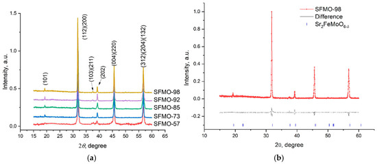
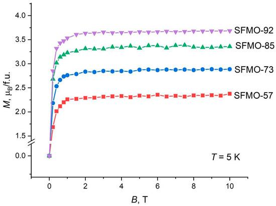
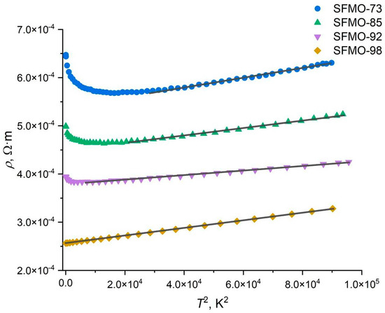
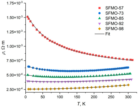
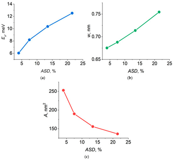
In this work, we consider the influence of antisite disorder, e.g., Fe ions on Mo sites, FeMo, and vice versa, MoFe, on the resistivity of strontium ferromolybdate ceramics fabricated by the solid-state reaction method. Strontium ferromolybdate ceramics fabricated via solid-state reactions exhibit a low-temperature minimum resistivity owing to the interplay between the bulk metallic resistivity of the grains, which increases with temperature and becomes dominant at higher temperatures, and an intergrain tunneling mechanism of charge carrier conduction, which leads to a decrease in conductivity with decreasing temperature in the low-temperature region. The parameters of the bulk metallic resistivity and fluctuation-induced intergrain tunneling were determined by fitting the experimental data to these resistivity models. The impact of antisite disorder on the resistivity parameters was considered. It turns out that antisite disorder affects the effective barrier height of intergrain tunneling and the effective values of the barrier width and the barrier area. Disorder increases the effective barrier height for intergrain tunneling, increases its barrier width, and decreases the effective barrier area of nanosized barriers. The results are discussed using experimental data available in the literature.
Full article

Figure 1
Open AccessArticle
Lattice Distortion, Band Gap and Band Tail in Heavily Doped In2O3:Sn and ZnO:Al Thin Films Annealed at Different Temperatures in Nitrogen
by
Cecilia Guillén
Electron. Mater. 2026, 7(1), 4; https://doi.org/10.3390/electronicmat7010004 - 28 Feb 2026
Abstract
►▼
Show Figures
Heavily doped metal oxide thin films combining high visible transmittance and low electrical resistance are used in a multitude of optoelectronic devices, where their performance is highly dependent on the structural defects and density of electronic states associated with doping. This study explores
[...] Read more.
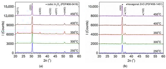
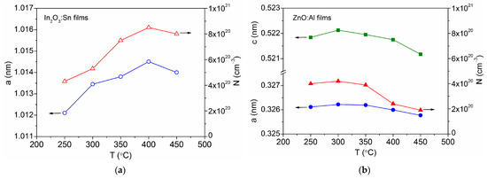
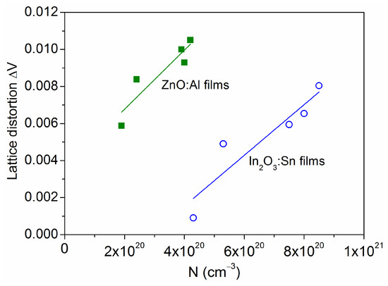
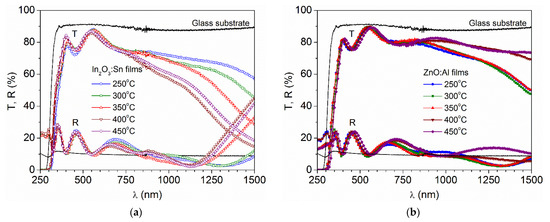
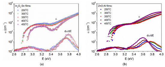
Heavily doped metal oxide thin films combining high visible transmittance and low electrical resistance are used in a multitude of optoelectronic devices, where their performance is highly dependent on the structural defects and density of electronic states associated with doping. This study explores the structural, optical, and electronic properties of Sn-doped indium oxide (In2O3:Sn) and Al-doped zinc oxide (ZnO:Al) thin films, which were prepared by sputtering on unheated glass substrates and subsequently annealed in N2 at different temperatures between 250 °C and 450 °C. These samples reach free electron densities above 1020 cm−3 due to the presence of extrinsic donors (mainly substitutional defects of SnIn and AlZn) and also intrinsic donors (oxygen vacancies), which change with the annealing temperature due to oxygen desorption and/or cation migration processes. The volume of the crystal lattice expands (up to a maximum of 1.1%) and the band gap widens (up to a maximum of 17.9%) with respect to the undoped material, increasing with electron density. Additional absorption is due to band tail, at an energy ~10% below the undoped band gap, which varies slightly with the carrier concentration. The same general behavior is observed for both materials, with particularities in terms of crystal lattice and electronic states, which can be tuned by the heating temperature.
Full article

Figure 1
Open AccessArticle
The Mixed Halogen-Ion Effect in Lead Silicate Glasses: A Correlative Study of Ionic Transport and Optical Spectroscopy in the 45PbO–xPbF2–(20−x)PbCl2–35SiO2 System
by
Manar Alenezi, Amrit Prasad Kafle, Meznh Alsubaie, Najwa Albalawi, Ian L. Pegg and Biprodas Dutta
Electron. Mater. 2026, 7(1), 3; https://doi.org/10.3390/electronicmat7010003 - 5 Feb 2026
Abstract
►▼
Show Figures
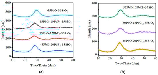
We present a fresh perspective on the mixed halogen-ion effect (MHE) in lead silicate glasses containing a mixture of halogen ions with a correlative study of optical spectroscopy and halogen ion transport. PbO was partially substituted by either PbCl2 or PbF2
[...] Read more.
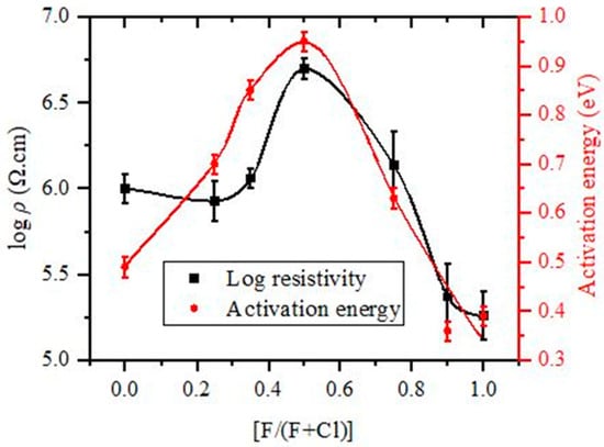
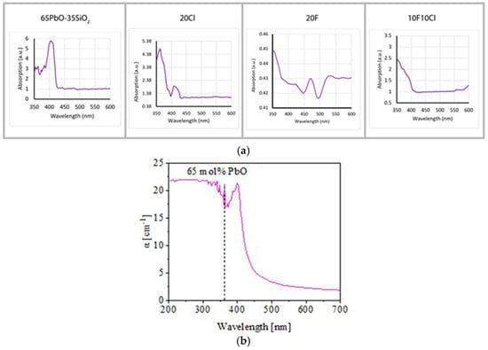
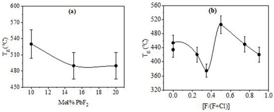
We present a fresh perspective on the mixed halogen-ion effect (MHE) in lead silicate glasses containing a mixture of halogen ions with a correlative study of optical spectroscopy and halogen ion transport. PbO was partially substituted by either PbCl2 or PbF2 in the ternary glass system: (65 − x) − x(PbF2 or PbCl2)-35SiO2 (where 0 ≤ x ≤ 20 mol%) and by a mixture of PbF2 and PbCl2 in the quaternary glass series: 45PbO − xPbF2 − (20 − x)PbCl2–35SiO2 (where 0 ≤ x ≤ 20 mol%). A suite of improved characterization techniques, including 4-probe van der Pauw resistivity measurements, optical absorption spectroscopy, differential thermal analysis, etc., was employed to correlate composition with physical properties. Replacing PbO with small quantities of PbF2 or PbCl2 in binary 65PbO-35SiO2 glass resulted in a dramatic increase in conductivity by 3–4 orders of magnitude, confirming a shift from Pb2+-mediated to halide ion-mediated conduction and, within the mixed-halogen series, a profound MHE was observed. Contrary to previously reported data, the activation energy for conduction and the resistivity both exhibited maxima at the mixed halogen-ion ratio, MHR = (F/(F + Cl), of 0.5. The glass transition temperature (Tg) exhibited a non-monotonic trend, peaking at 506 °C for the MHR = 0.5 composition. Optical absorption measurements have revealed that the MHR = 0.5 glass has the broadest absorption edge and also exhibits certain features in the near IR region of the Urbach tail, which are suggestive of maximum electronic disorder.
Full article

Figure 1
Open AccessArticle
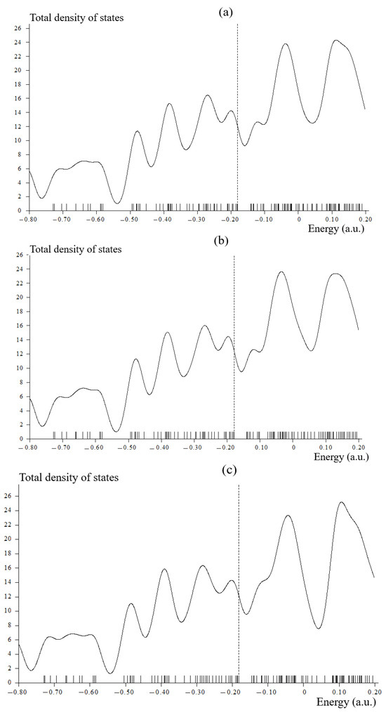
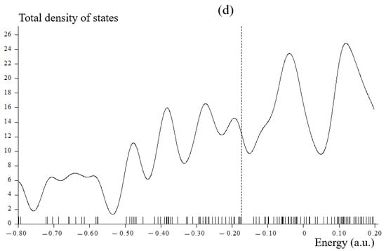
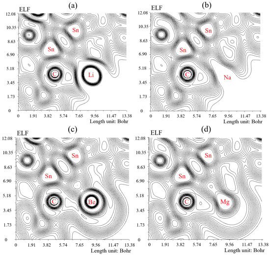
Modeling SnC-Anode Material for Hybrid Li, Na, Be, Mg Ion-Batteries: Structural and Electronic Analysis by Mastering the Density of States
by
Fatemeh Mollaamin and Majid Monajjemi
Electron. Mater. 2026, 7(1), 2; https://doi.org/10.3390/electronicmat7010002 - 1 Jan 2026
Abstract
►▼
Show Figures
The increasing demand for next-generation rechargeable batteries that offer high energy density, a long lifespan, high safety, and low cost has led to a need for better electrode materials for lithium-ion batteries. This also involves developing alternative storage systems using common resources such
[...] Read more.
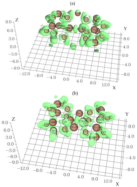
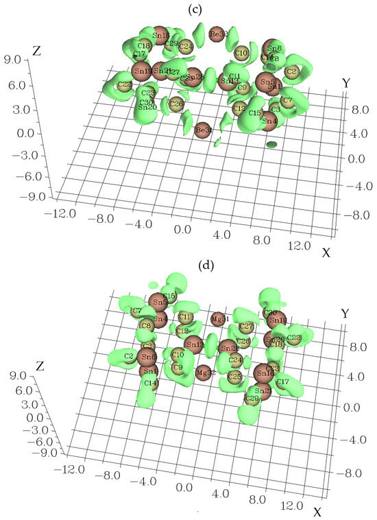
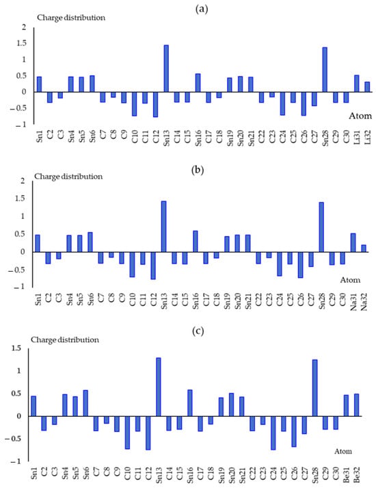
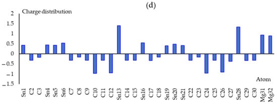
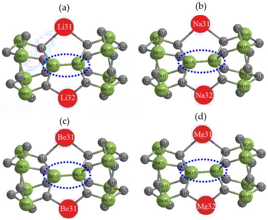
The increasing demand for next-generation rechargeable batteries that offer high energy density, a long lifespan, high safety, and low cost has led to a need for better electrode materials for lithium-ion batteries. This also involves developing alternative storage systems using common resources such as sodium-ion batteries, beryllium-ion batteries, or magnesium-ion batteries. Tin carbide (SnC) is highly promising as an anode material for lithium, sodium, beryllium, and magnesium ion batteries due to its ability to form nanoclusters like Sn(Li2)C, Sn(Na2)C, Sn(Be2)C, and Sn(Mg2)C. A detailed study was done using computational methods, including analysis of charge density differences, total density of states, and electron localization function for these hybrid clusters. This research suggests that SnC could be useful in multivalent-ion batteries using Be2+ ions because its properties can match or even exceed those of monovalent ions. The study also shows that the maximum capacity, stability energy, and ion movement in these materials can be understood by looking at atomic-level properties like the coordination between host atoms and ions. Recent findings on using tin carbide in these types of batteries and methods to improve their performance have been discussed.
Full article

Figure 1
Open AccessReview
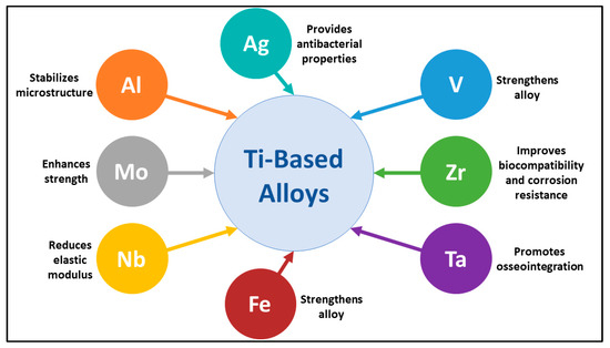
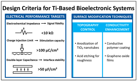
Titanium Alloys at the Interface of Electronics and Biomedicine: A Review of Functional Properties and Applications
by
Alex-Barna Kacsó, Ladislau Matekovits and Ildiko Peter
Electron. Mater. 2026, 7(1), 1; https://doi.org/10.3390/electronicmat7010001 - 1 Jan 2026
Cited by 2
Abstract
►▼
Show Figures
Recent studies show that titanium (Ti)-based alloys combine established mechanical strength, corrosion resistance, and biocompatibility with emerging electrical and electrochemical properties relevant to bioelectronics. The main goal of the present manuscript is to give a wide-ranging overview on the use of Ti-alloys in
[...] Read more.
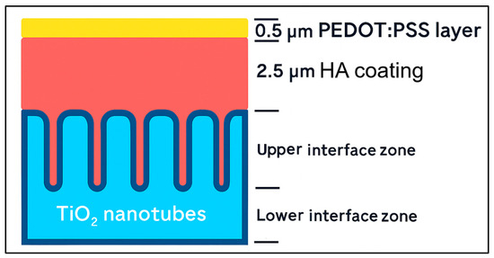
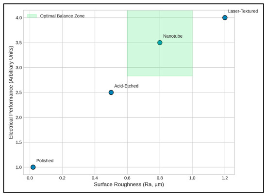
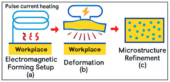
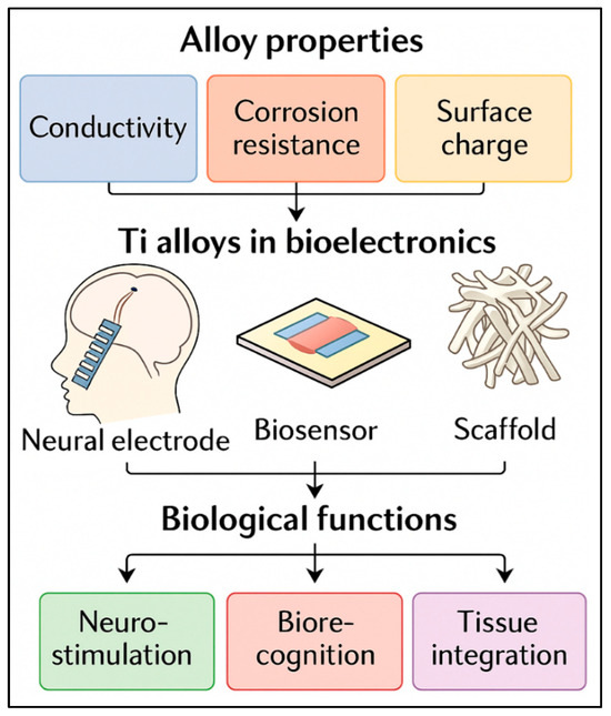
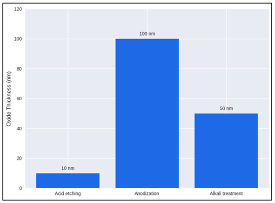
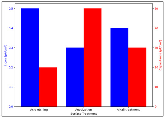
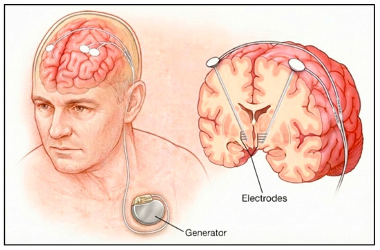
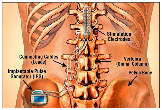
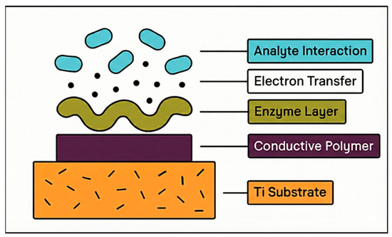
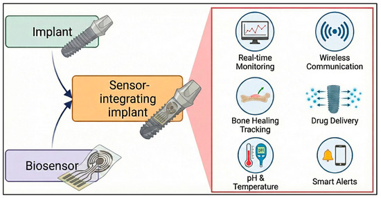
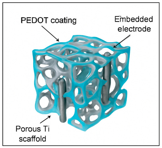
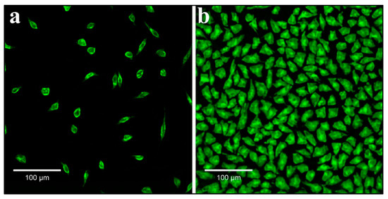
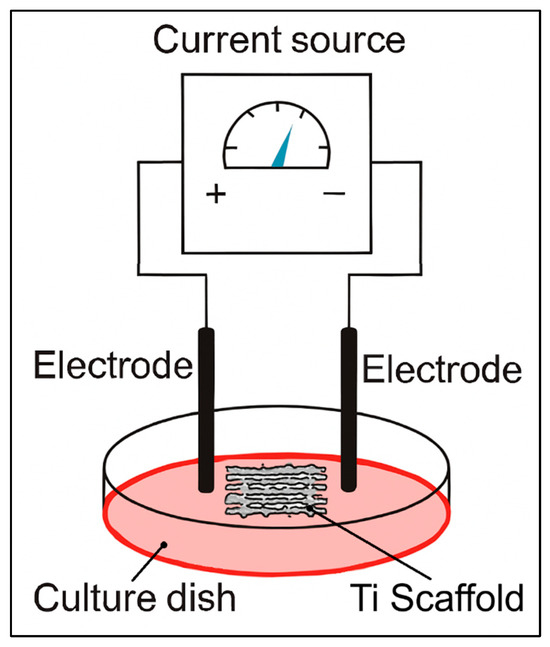
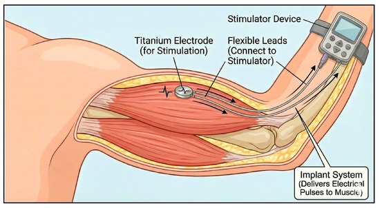
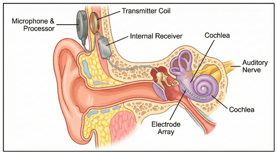
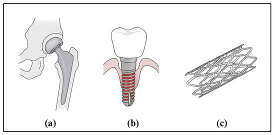
Recent studies show that titanium (Ti)-based alloys combine established mechanical strength, corrosion resistance, and biocompatibility with emerging electrical and electrochemical properties relevant to bioelectronics. The main goal of the present manuscript is to give a wide-ranging overview on the use of Ti-alloys in electronics and biomedicine, focusing on a comprehensive analysis and synthesis of the existing literature to identify gaps and future directions. Concurrently, the identification of possible correlations between the effects of the manufacturing process, alloying elements, and other degrees of freedom influencing the material characteristics are put in evidence, aiming to establish a global view on efficient interdisciplinary efforts to realize high-added-value smart devices useful in the field of biomedicine, such as, for example, implantable apparatuses. This review mostly summarizes advances in surface modification approaches—including anodization, conductive coatings, and nanostructuring that improve conductivity while maintaining biological compatibility. Trends in applications demonstrate how these alloys support smart implants, biosensors, and neural interfaces by enabling reliable signal transmission and long-term integration with tissue. Key challenges remain in balancing electrical performance with biological response and in scaling laboratory modifications for clinical use. Perspectives for future work include optimizing alloy composition, refining surface treatments, and developing multifunctional designs that integrate mechanical, biological, and electronic requirements. Together, these directions highlight the potential of titanium alloys to serve as foundational materials for next-generation bioelectronic medical technologies.
Full article

Figure 1
Open AccessArticle
Image Enhancement Algorithm and FPGA Implementation for High-Sensitivity Low-Light Detection Based on Carbon-Based HGFET
by
Yi Cao, Yuyan Zhang, Zhifeng Chen, Dongyi Lin, Chengying Chen, Liming Chen and Jianhua Jiang
Electron. Mater. 2025, 6(4), 23; https://doi.org/10.3390/electronicmat6040023 - 2 Dec 2025
Abstract
►▼
Show Figures
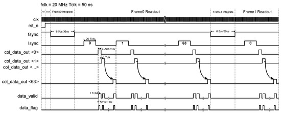
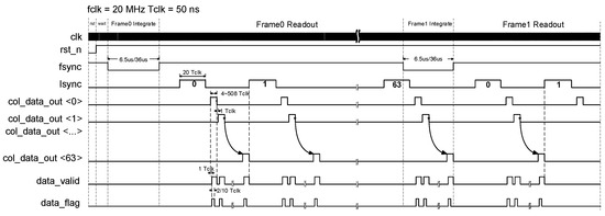
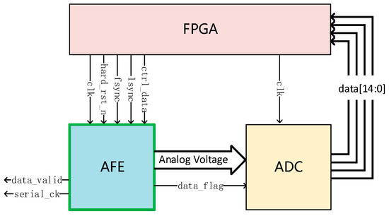
To address the issues of insufficient responsivity and low imaging contrast of carbon-based HGFET high-sensitivity short-wave infrared (SWIR) detectors under low-light conditions, this paper proposes a high-sensitivity and high-contrast image enhancement algorithm for low-light detection, with FPGA-based hardware verification. The proposed algorithm establishes
[...] Read more.
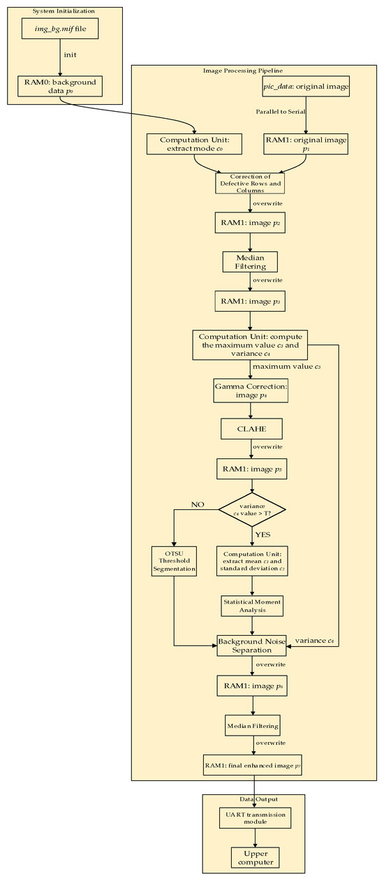
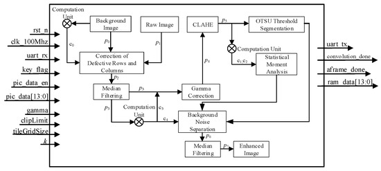
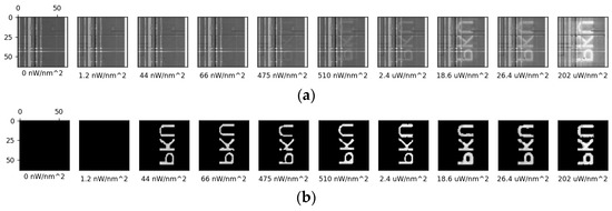
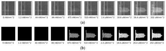
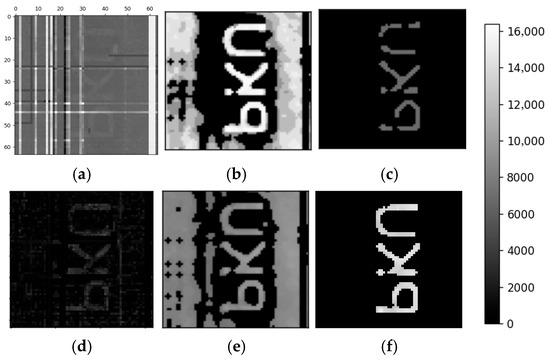
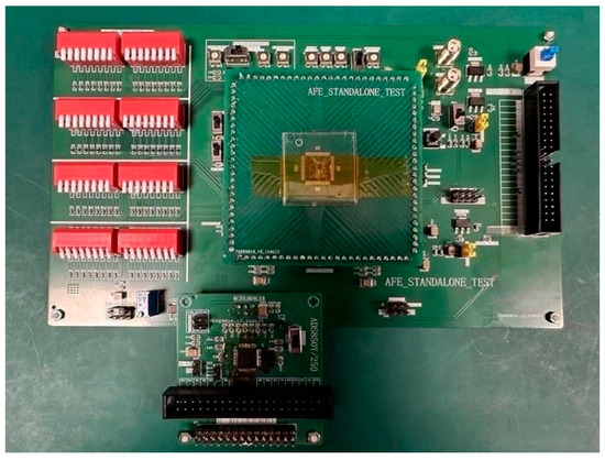
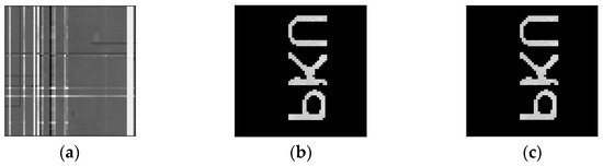
To address the issues of insufficient responsivity and low imaging contrast of carbon-based HGFET high-sensitivity short-wave infrared (SWIR) detectors under low-light conditions, this paper proposes a high-sensitivity and high-contrast image enhancement algorithm for low-light detection, with FPGA-based hardware verification. The proposed algorithm establishes a multi-stage cooperative enhancement framework targeting key challenges such as low signal-to-noise ratio (SNR), high dark-state noise, and weak target extraction. Unlike traditional direct enhancement methods, the proposed approach first performs defective row-column correction and background noise separation based on dark-state data, which provides a clean foundation for signal reconstruction. Furthermore, an adaptive gamma correction mechanism based on image maximum value is introduced to avoid unnecessary nonlinear transformations in high-contrast regions. During the contrast enhancement stage, an exposure-constrained adaptive histogram equalization strategy is adopted to effectively suppress noise amplification and saturation in low-light scenes. Finally, an innovative dual-mode threshold selection method based on image variance is proposed, which can dynamically integrate the OTSU algorithm with statistical moment analysis to ensure robust background noise separation across both high- and low-contrast scenarios. Experimental results demonstrate that the proposed algorithm significantly improves target contrast in infrared images while preventing detail loss due to overexposure. Under microwatt-level laser power, background noise is effectively suppressed, and both imaging quality and weak target detection capability are substantially enhanced.
Full article

Figure 1
Open AccessArticle
Integration of Silicon PIN Detectors and TENGs for Self-Powered Wireless AI Intelligent Recognition
by
Junjie Tang, Huafei Wang, Maoqiu Pu, Penghui Luo, Min Yu and Zhiyuan Zhu
Electron. Mater. 2025, 6(4), 22; https://doi.org/10.3390/electronicmat6040022 - 2 Dec 2025
Abstract
►▼
Show Figures
In this study, we explore the integration of a cost-effective triboelectric nanogenerator (TENG) with an large silicon PIN detector (diameter: 12 mm) for intelligent wireless recognition applications. Wireless communication eliminates the need for physical connections, enabling greater flexibility and scalability in deployment. It
[...] Read more.
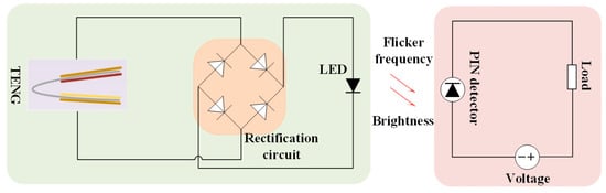
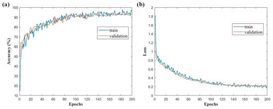
In this study, we explore the integration of a cost-effective triboelectric nanogenerator (TENG) with an large silicon PIN detector (diameter: 12 mm) for intelligent wireless recognition applications. Wireless communication eliminates the need for physical connections, enabling greater flexibility and scalability in deployment. It allows for seamless integration of AI systems into a wide range of environments without the constraints of wiring, reducing installation complexity and enhancing mobility. Additionally, we demonstrate the TENG’s functionality as an autonomous communication unit. The TENG is employed to convert various environmentally triggered signals into digital formats and to autonomously power optoelectronic devices, thus eliminating the need for an external power supply. By integrating optoelectronic components within the self-powered sensing system, the TENG can identify specific trigger information and reduce extraneous noise, thereby improving the accuracy of information transmission. Moreover wireless technology facilitates real-time data transmission and processing. This setup not only enhances the overall efficiency and adaptability of the system but also supports continuous operation in diverse and dynamic settings. This paper introduces a novel convolutional neural network-long short-term memory (CNN-LSTM) fusion neural network model. Utilizing the sensing system in combination with the CNN-LSTM neural network enables the collection and identification of variations in the flicker frequency and luminosity of optoelectronic devices. This capability allows for the recognition of environmental trigger signals generated by the TENG. The classification and recognition results of human body trigger signals indicate a recognition accuracy of 92.94%.
Full article

Figure 1
Highly Accessed Articles
Latest Books
E-Mail Alert
News
Topics
Topic in
Electronic Materials, IJMS, Magnetochemistry, Materials, Nanomaterials
Magnetic Nanoparticles and Thin Films
Topic Editors: Renat F. Sabirianov, Ahmad AlsaadDeadline: 31 December 2026
Topic in
Electronic Materials, Materials, Nanomaterials, Polymers, Sensors, Sci, Biosensors, Micromachines
Advanced Materials for Flexible and Wearable Electronics
Topic Editors: Javad Foroughi, Yan WangDeadline: 30 May 2027
Topic in
AI Materials, Electronic Materials, Energies, Materials, Nanoenergy Advances, Nanomaterials, Solar, Sci
Emerging Materials and Technologies for Energy Applications
Topic Editors: Susana Fernández, Fernando B. NaranjoDeadline: 30 June 2027
Topic in
Eng, J. Compos. Sci., Materials, Textiles, Electronic Materials, Micromachines
Flexible and Wearable Self-Powered Sensor Materials for Vibration Monitoring in Mechanical Systems
Topic Editors: Trilochan Bhatta, Puran PandeyDeadline: 31 August 2027
Special Issues
Special Issue in
Electronic Materials
Advances in Magnetic Semiconductor Materials
Guest Editor: Yilin WangDeadline: 30 September 2026
Special Issue in
Electronic Materials
Emerging Trends in Electronic Materials and Functional Nanostructures
Guest Editor: Zongjie ShenDeadline: 31 December 2026
Special Issue in
Electronic Materials
Electronic Materials for Nuclear Science and Radiation Technologies: Defects, Properties and Applications
Guest Editors: Qiang Zhao, Zheng ZhangDeadline: 31 January 2027
Special Issue in
Electronic Materials
Advanced and Emerging Inorganic Semiconductor Materials
Guest Editor: Wojciech PisulaDeadline: 31 March 2027