1. Introduction
Recently, organic polymers have drawn considerable attention from researchers for their promising opto-electronics properties. Organic materials have advantages over inorganic materials due to the fact of their low cost and high availability [
1]. In addition, due to the decrease in fossil fuels and similar energy sources, which are being reduced day by day, this inherently generates the requirement to develop renewable energy technologies. Over the last few decades, organic dye-based devices have gained much importance due to the fact of their easy fabrication techniques and numerous advantages over conventional silicon-based crystalline devices [
2,
3,
4,
5,
6,
7]. For a superior diode, the asymmetry (i.e., rectification ratio), nonlinearity and response capacity should be large, and this can be achieved via thermionic emission and quantum mechanical tunneling [
8]. Therefore, it is undoubtedly very important to select different dyes to better improve the electrical parameters of devices and to use them as an alternative to inorganic diode-like devices. Dyes have the potential to play a role as a photosensitizer, and they also possess several excellent film-forming properties. Donor–acceptor (D-A)-type chromophores with a low band gap are particularly of interest. The band gap levels and other optoelectronic properties of the chromophores can easily be tuned. Since naturally occurring curcumin behaves as a donor–acceptor–donor (D-A-D) chromophore [
9], turmeric (curcumin)-based natural dye was introduced in the present work for use in the formation of an Al/turmeric/Cu device. The advantages of choosing curcumin as a barrier are the following: (i) It is known that a thin dielectric between two metal layers forms a parallel plate capacitor of high capacitance with a large time constant (TC). This means the maximum operating frequency will have a small value when applied in communication systems. This is not sufficient for acceptance in devices used for high-speed communication. (ii)However, curcumin has a small dielectric constant (k) [
10], which reduces the capacitance of the device, and the electroluminescent peak emission for curcumin occurs at a wavelength of 612 nm. (iii) In comparison to other chromophores, it is less expensive, compatible and naturally available nontoxic dye [
11]. The main focus of this experiment was whether this device could behave as a superior diode with acceptable rectifying characteristics. In this present work, it was found that these dye-based devices behaved like a diode. The diode using natural dye (i.e., turmeric) may be treated as a metal insulator metal diode or a Schottky diode. Two distinct mechanisms are discussed to explain its electrical conduction properties in this investigation. The aforementioned mechanisms are explained by the following theories while also observing a high rectification ratio with very low resistance by the proposed device: (i) quantum mechanical tunneling theory on metal–insulator–metal diodes; (ii) thermionic emission (TE) theory on Schottky barrier diodes. At low temperature, the dominant current conduction occurs due to the fact of quantum mechanical tunneling, whereas thermionic emission holds at high temperature. In this device, the insulator material, metals, thickness of the insulating layer and the band gap of the chromophore decided the mechanism that dominated.
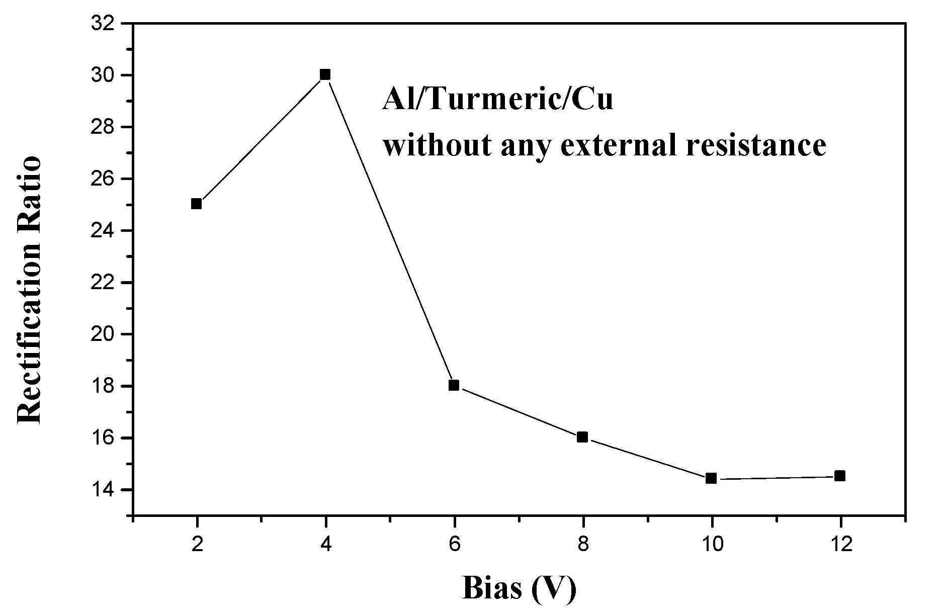
The detailed fabrication and characterization of the Al/turmeric/Cu diode are presented here in this work. The outcomes of the experiment showed excellent results in improving the rectification ratio of the device. Our observations show that our achieved rectification ratio (i.e., asymmetry) was 30 at the 4 V bias voltage, indicating enormous improvement over the previous highest reported rectification ratio of 10 at 3 V for a double-insulator layer MIIM device [
8]. Our observations also lead to us to conclude that the series resistance of the device decreases with temperature.
3. Results and Discussion
This device works in such a way that when a current is passed through these two layers of metal, the electrons are induced to quantum mechanically tunnel from one piece of metal to another piece, passing through the thin insulator placed between them at very low voltage. When the electrodes with different barrier heights, as well as different work functions (i.e., 4.26 and 5.10 eV for Al and Cu, respectively) were used, an internal electric field will build-up resulting from a built-in voltage (V
bi),which equals the difference in the work function of the electrodes. Therefore, when voltage is applied across the metal insulator metal diode, electrons preferentially make a tunnel in one particular direction over the other, therefore resulting in the formation of a diode [
12].
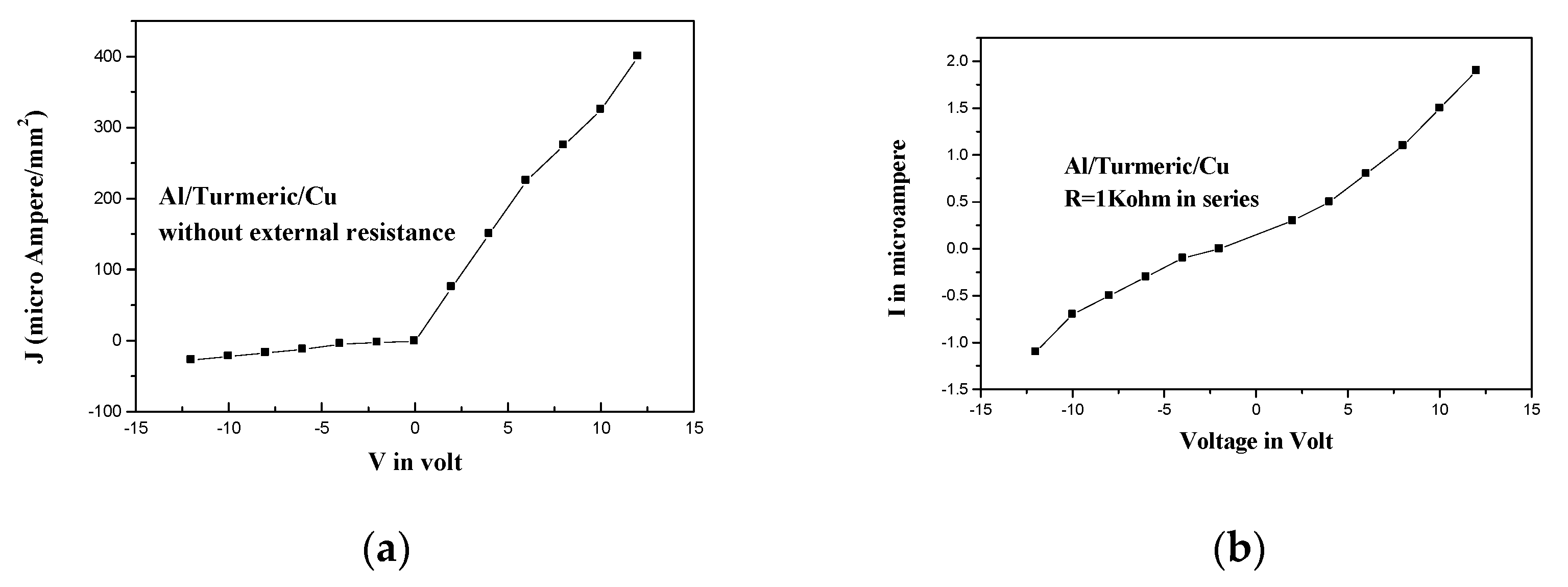
Figure 1a,b. shows the current voltage characteristics of the Al/turmeric/Cu device for resistance R = 0 and R = 1 KΩ, respectively, performed at room temperature. These characteristics indicate a nonlinear, asymmetric behavior with a high rectification ratio. If this device is considered a metal–insulator–metal (MIM) tunnel diode, a quantum mechanical tunneling action takes place. Quantum mechanical tunneling depends on the metal structure, and a small area of the metal’s surface induces a low tunneling voltage with a higher tunneling current [
13]. A thin turmeric layer was deposited between the aluminum and copper plates. The flow of electron occurred from one metal to another through the insulating layer (i.e., turmeric) by field-effect tunneling. This tunneling probability is controlled by the contact area of the metals and the bias voltage. In this device, at very low temperatures, the current conduction mechanism is dominated by quantum tunnelling. The energy band diagram depends on the work function of metals (4.20, 5.10), electron affinity of curcumin (1.9–2.4 eV) [
14] and the band gap of curcumin (2.6 eV). For a negative bias, the shape of the energy band diagram is altered, as shown in
Figure 2. From
Figure 2. it can be seen that electrons in Cu may tunnel into the vacant states of Al. For a very thin turmeric layer, there is the occurrence of quantum tunnelling of electrons. This tunnelling probability depended on the applied voltage: when this bias voltage increased, there was a decrease in the width of the insulating layer near the Fermi level. Therefore, there was an increase in the tunnel current due to the decrease in the tunnel distance. When a positive voltage was applied to the device, the same phenomenon occurred. In this case, the tunnelling occurred from the Al to Cu. Here, for a voltage above the barrier height, the current also increased with the decrease in the tunnelling distance. Thus, the work function difference was the main reason for the asymmetric behavior of the I-V characteristic for the Al/turmeric/Cu device [
15].
In this device, the current conduction occurred either by quantum tunnelling or by Schottky emission. We know that for any organic material, the current conduction is governed by different mechanisms. For MIM diodes, the tunnelling current should be directly proportional to the bias voltage for a bias voltages less than the barrier height and should increase exponentially with voltages when the bias becomes comparable to the barrier height. For this work, there were 1.85 eV barrier heights along the Al/turmeric contact, and there was ohmic behavior at the Cu/turmeric contact.
In the present device, the current conduction mechanism occurred due to the fact of quantum tunnelling and thermionic emission. At very low temperatures (below 170 K), when turmeric (curcumin) behaves like an insulator, then quantum tunnelling is dominant over thermionic emission. Here, the tunnelling occurs between two dissimilar work function metals, Al (4.20) and Cu (5.10), separated by a turmeric layer. In the current conduction mechanism, electrons faced nonidentical barriers because of the work function difference between Al and Cu. The voltage applied to Al and Cu was grounded for biasing the device. With 1 kΩ resistance in the series and a temperature below 190K in this device, direct tunnelling (DT) dominated for low forward and low reverse bias, where the applied bias was less than the barrier height. On the other hand, for high forward and high reverse bias, this meant that when the bias voltage was greater than the barrier height, then the current conduction was dominated by Fowler–Nordheim tunnelling (FNT) [
16]. However, the temperature-dependent I-V, displayed in
Figure 3, shows that thermionic emission was dominant over quantum tunnelling in the current conduction mechanism of this device.
Figure 1a and
Figure 3 demonstrate the temperature-dependent I-V characteristics of the Al/turmeric/Cu device at room temperature and above.
Figure 1a shows that the I-V characteristics were nonlinear and asymmetric with a very low turn on voltage (below 1V). This nonlinear asymmetric behavior can be explained with the junction resistance and interface states of junction. Due to the different injection directions, the energy barrier of this device was asymmetric. The barrier varied with the bias voltage due to the injection of electrons from curcumin; on the other hand, when electrons were injected from cathode (Cu), the barrier height remained constant. When a positive voltage was applied, the Al/curcumin barrier decreased and electrons were transported through the junction. When a negative voltage was applied, the electron transportation was controlled by the Cu/curcumin barrier. If the turmeric (curcumin) behaves like an organic semiconductor, then the depletion layer at the junction is to be decreased at forward bias and increased at reverse bias. As a result, the ampere–volt (I-V) characteristic is to be nonlinear and asymmetric. Therefore, the device then behaves like a Schottky diode, and the current of the device is obtained due to the thermionic emission, and it is given by Equations (1) and (2) [
17]:
where
I0 is the reverse saturation current and given as Equation (2):
where
A is the contact area of the device.
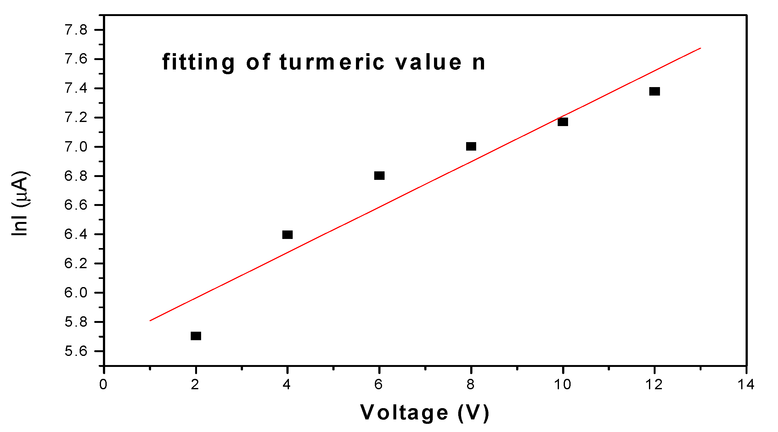
The reverse saturation current is derived from the straight line intercept of ln (I) at a zero bias voltage. To evaluate the rectification behavior of the device, the I-V characteristics were measured under ambient condition, as shown in
Figure 1a,b, and the asymmetry, nonlinearity, and sensitivity of the device were extracted from this I-V. The characteristics show the rectifying property of the device was in a nonlinear manner. The rectification ratio (RR) is determined from the ratio of the forward current to the reverse current at a certain applied voltage. In this experiment, we observed that the rectification ratio varied with the applied voltage. For this Al/turmeric/Cu junction device, the maximum value of the rectification ratio was found to be 30 at 4 V.
Figure 4 shows the variation in the rectification ratio (RR) with the applied voltage (V). Ideality factor n is the most important parameter of the diode, which is calculated using the following Equation (3) [
18]:
where
V is the applied voltage;
T is the temperature in Kelvins. The value of the ideality factor for an ideal diode is to be 1. For a real Schottky diode, the value of the ideality factor is greater than 1. In this experiment, the value of the ideality factor was found to be approximately 6.56. It is quite normal to have a high value of ideality factor for herbal and organic devices because of their disordered amorphous nature. This greater value of ideality factor might be explained from the recombination of electrons and holes in the depletion region, and it is also associated with Fermi-level pinning at the interface region. In this device, the thickness of the dye layer was greater in comparison to the normal Schottky diode. The greater thickness of the curcumin layer led to a huge recombination of electrons and holes. Therefore, probable reasons for the high values of the ideality factor of the devices are a potential drop in the interfacial layer, the presence of excess current and a high recombination current through the interfacial states between the metal curcumin layers [
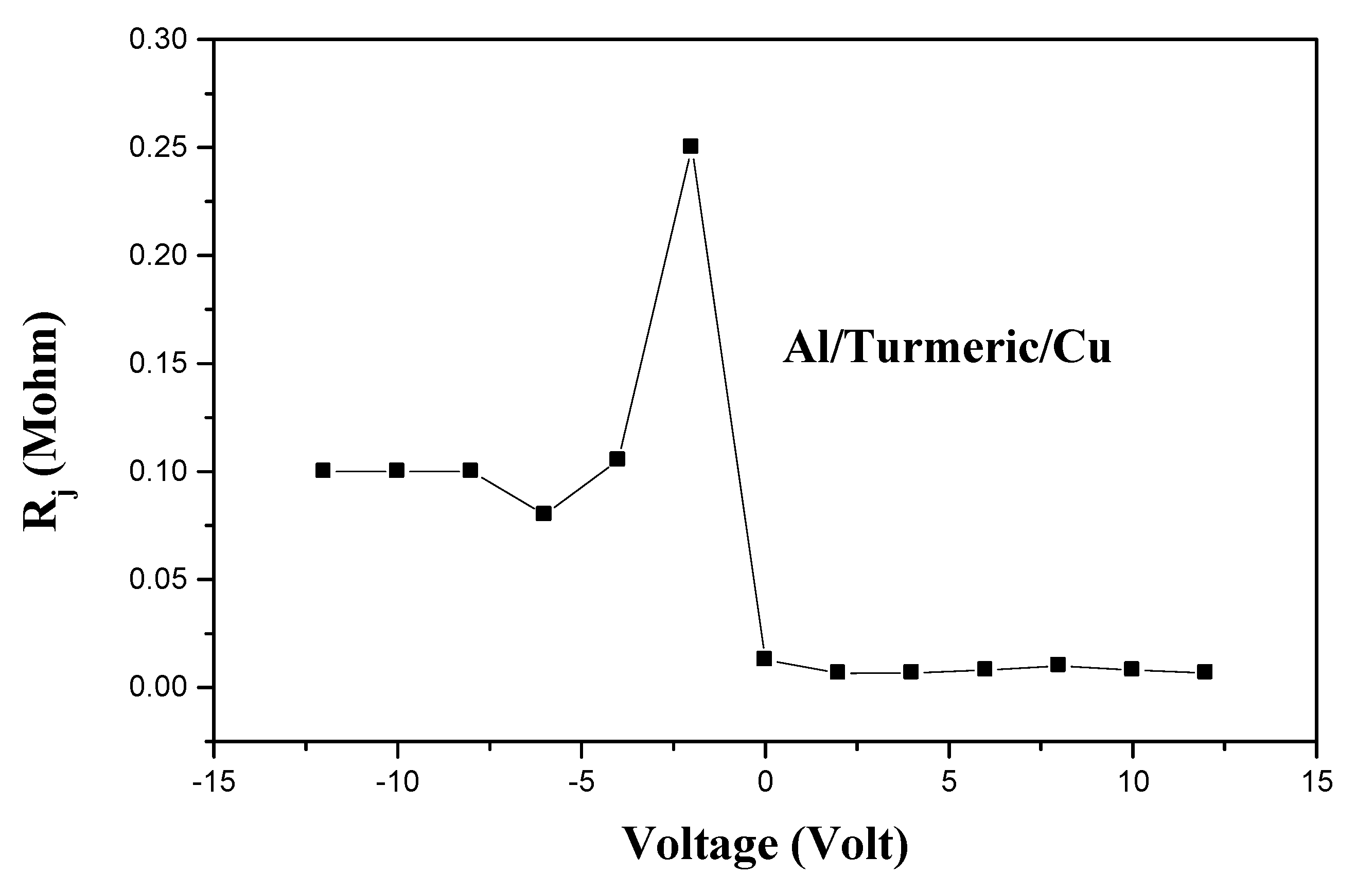
19]. It was observed for this device that the values for R
s and R
sh were 8 and 100 KΩ, respectively. Using
Figure 2 and
Figure 5 we have calculated the values of R
s and n.
It was observed that the I-V characteristics varied from diode to diode. At first, we fabricated the device for the I-V characteristics, and we conducted an experiment. Then, after one month, we fabricated another device and performed an experiment for temperature-dependent I-V. For these two I-Vs, we used two different Al/turmeric/Cu devices with different contact areas (i.e., 4 and 2.2 mm
2) and different thicknesses. Because of this, there was a change in the current fortwo different I-V characteristics. The temperature-dependent current–voltage (I-V) measurements were performed over a temperature range of 28–65 °C. From
Figure 3 we observed that the I-V characteristics changed very much with the temperature for the Al/turmeric/Cu device. This shows that in our device, thermionic emission dominated over quantum tunneling. The values of the series resistance changed from 0.056 MΩ (at 65 °C) to 1.1 MΩ (at 28 °C). When the temperature was below 190 K, turmeric behaved like an insulator, and the device was like an MIM diode. At room temperature and above, when the thermal energy of the electron was greater than the band gap of curcumin, then the turmeric behaved like a semiconductor and the device was a Schottky diode. If we consider turmeric as n-type semiconductor, then the Schottky junction formed between the Al and turmeric. Before the contact formation, the Fermi level of turmeric was higher than Al, but after the formation of contact, the Fermi levels must line up at equilibrium, which means there was a conduction of electrons from the conduction band of the turmeric to empty energy states above the Fermi level of Al. Due to the fact of this motion of electrons, there were positive charges on the turmeric side and electrons on the Al side, which formed an electric field directed from turmeric to Al. After the formation of the Al-turmeric junction, electrons were not only conducted from the surface of the turmeric but also from a certain depth. Because of this, there was the formation of a depletion region at the Al/turmeric junction. When the temperature of the device increased, the thermal energy of the electrons increased, and the depletion layer decreased. As a result, the current increased and the series resistance decreased with the temperature. The current transport across the metal semiconductor junction was a temperature-activated process; because of this, electrons at low temperatures were able to surmount the lower barriers and the current transport was dominated by current flowing through the paths of the lower Schottky barrier height with a large ideality factor.
However, the problem with this device is one of stability, as the load current decreases over time. To reduce this problem, the authors suggest using an electrolyte. In that case, the holes will be filled by electrons from electrolyte ions, helping to conduct the current between the cathode and the dye molecule. Another problem with this device is its trap energy, which we have discussed in detail in our earlier papers [
20,
21,
22].


