Proceeding Paper

Evanescent-Wave Gas Sensing Using an Integrated Thermal Light Source †

1
CTR Carinthian Tech Research AG, Villach, Austria
2
Infineon Technologies Austria AG, Villach, Austria
3
Institute for Microelectronics and Microsensors, Johannes Kepler University, Linz, Austria
*
Author to whom correspondence should be addressed.
Presented at the Eurosensors 2017 Conference, Paris, France, 3–6 September 2017.
Proceedings 2017, 1(4), 550; https://doi.org/10.3390/proceedings1040550
Published: 17 August 2017
(This article belongs to the Proceedings of Proceedings of Eurosensors 2017, Paris, France, 3–6 September 2017)

Abstract

:
The last years showed an increased request for miniaturised, CMOS-compatible gas detectors. In contrast to sensors utilizing metal-oxide chemical interfaces, optical strategies are potentially faster and more robust. Recently we demonstrated CO2 detection by evanescent-wave absorption in the mid-infrared using a combination of an external laser source and silicon waveguides based on CMOS technology. We now go one step further and demonstrate the feasibility of detection of CO2 down to a concentration of 3% with a low-cost integrated thermal source. These results are promising for further technological developments towards on-chip mid-infrared photonic gas sensors, and new designs are currently devised to increase the yet relatively low sensitivity.

1. Introduction

CMOS-compatible gas sensors are of interest because of their potential use in portable devices and in automotive applications. Among the sensing approaches, optical techniques in the infrared fingerprint region of the investigated substance are particularly promising because of their high selectivity. The possibility to use photonic structures like waveguides for evanescent-wave absorption sensing was recently discussed for liquids [1]. Recently we also demonstrated that silicon waveguides with sub-wavelength dimensions can be used as sensing units for carbon dioxide detection [2]. In the previous experiments, a narrow-band laser beam, tuned to the frequency of maximum CO2 absorption, was used as a light source. An external laser source has multiple advantages over thermal sources, among them the very narrow emission line and the high peak intensity, it is however bulky and expensive. Another approach consists in developing quantum-cascade lasers on silicon. Such systems have been recently realized for the first time, with emission in a different spectral region [3] and might become an alternative to conventional thermal sources in the future. Nevertheless, the ease of fabrication and integration, the long-term stability and the low cost of production make integrated thermal emitters the preferable light source for the consumer electronics market.
Here we build on our previous findings by replacing the external laser source with an integrated thermal source, whose light is butt-coupled in a short silicon slab-waveguide (Figure 1a). When the medium to be sensed comes in proximity of the waveguide, the evanescent tail of the guided field is partially absorbed and a decrease in the transmitted light intensity is observed. The intensity decrease depends both on the amount of absorbing substance and on the waveguide parameters through the evanescent-field ratio (EFR), i.e., the ratio of the guided field extending outside the waveguide.
Here, after experimental determination of the EFR of our structures, we use an integrated emitter to measure the transmittance through the waveguide as a function of CO2 concentration and to determine the waveguide sensitivity. Our results show the feasibility of CO2 detection with an integrated light-source and a silicon slab-waveguide down to a concentration of 3%.

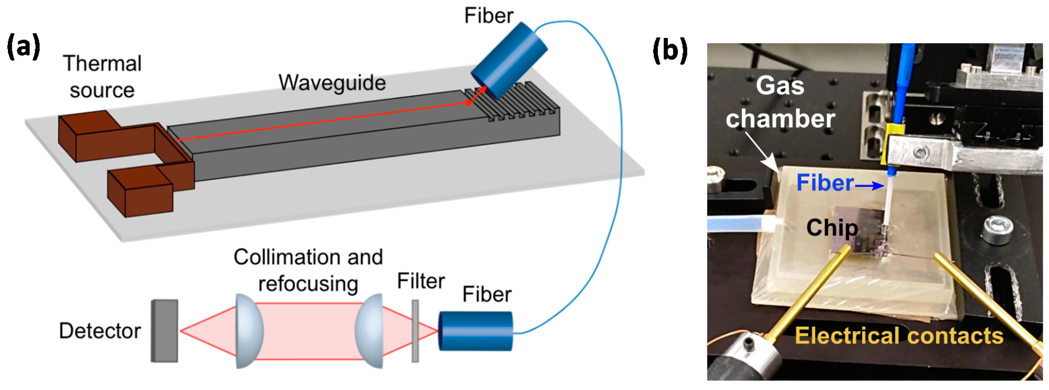
2. Material and Methods

The investigated structures are schematically depicted in Figure 1a and are composed of two units: the light source and the waveguide. The light source is a simple polysilicon heater. The heater is contacted with metal tips and supplied with current pulses of 6–7 mA with a repetition rate of 33 Hz and a duty cycle of 50%. The sensing unit is a polysilicon slab-waveguide fabricated on a silicon nitride membrane and a silicon oxide layer with a standard MEMS process by Infineon Technologies Austria AG. The silicon substrate below the waveguide is plasma etched and the silicon oxide is wet etched to form a honeycomb structure, in order to decrease the overlap between the evanescent field and the substrate materials. The details of the fabrication can be found in reference [2].
The heater, which lies in close proximity to the waveguide, has front dimensions that match the cross-section of the waveguide, and the infrared (IR) light is butt-coupled into the waveguide. On the other end of the waveguide, a grating coupler allows for out-coupling the radiation. The grating period is designed for an out-coupling angle of 30° with respect to the waveguide normal, and the out-coupled light is collected with a ZrF4 optical fiber (Thorlabs, 450 µm core diameter) located at a distance of a few tens of microns from the grating surface. The optical fiber conveys the light to the detection unit, which is composed of collimation and refocusing optics and a thermoelectrically cooled mercury-cadmium-telluride detector (Vigo Systems). The signal readout is performed with a lock-in amplifier (Princeton Instruments) and an oscilloscope. An optical bandpass filter, centered at 4.27 µm with a 180 nm bandwidth at a full-width at a half maximum (Spectrogon), is placed between the fiber and the detector. In a future design, a filter structure with similar performances will be integrated in the chip design. The optical path between fiber and detector is in air, and a commercial CO2 detector monitors the CO2 concentration in the air path. No significant variation in the CO2 concentration was observed during the measurements.
The sensor chip is placed in a small gas chamber (Figure 1b) that is continuously flushed with a mixture of CO2 (Linde, CO2 4.5) and N2 (Linde, N2 5.0) gas. The chamber has two apertures on the top, intended for inserting the electrical connections and the optical fiber, that also function as exit path for the gas. The concentration of the two gases in the mixture is controlled by a mass-flow-control unit, and the gas flows at a speed of 100 mL/min. No change in the measured transmittance was observed by reducing the flow speed to smaller values.

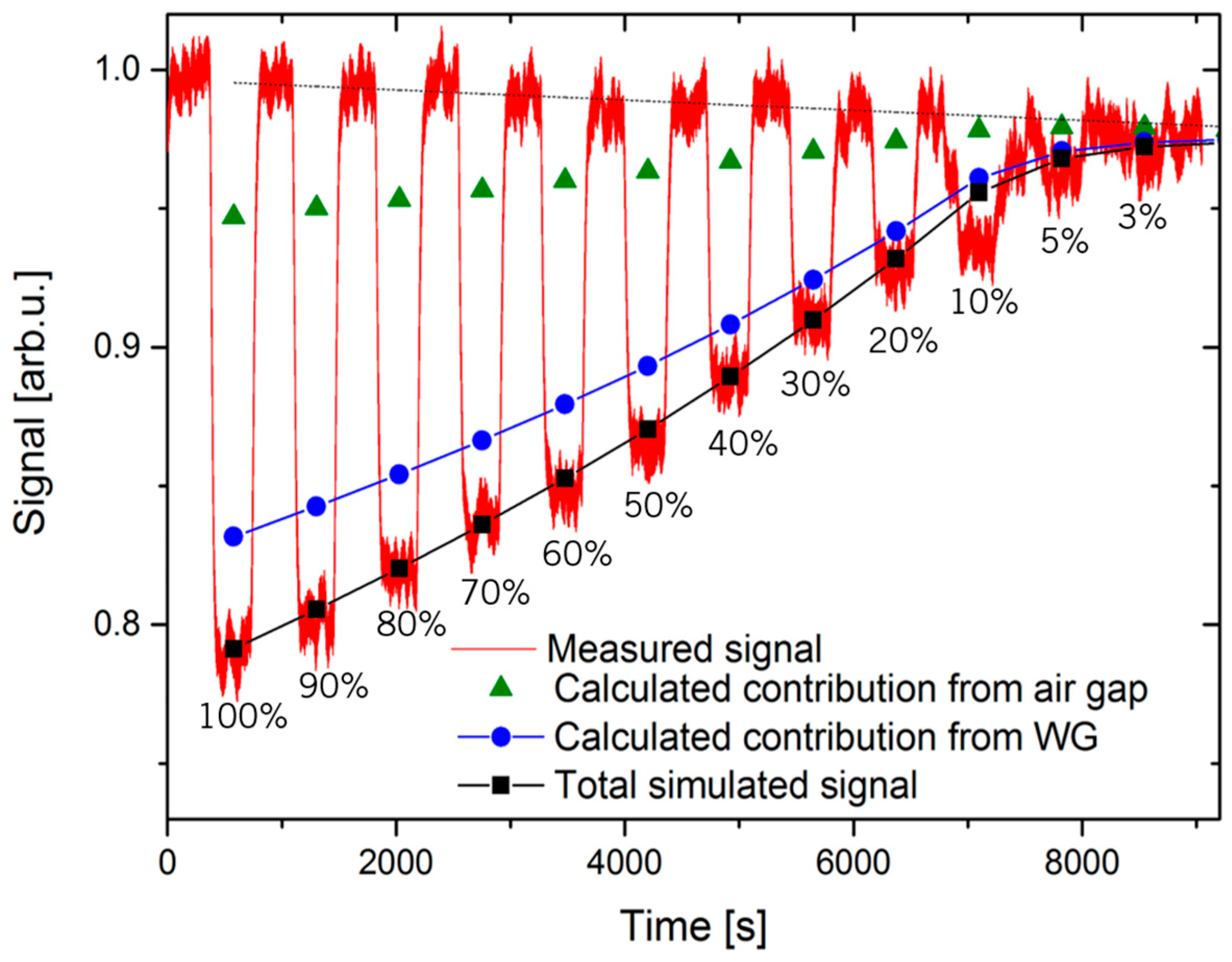
3. Results and Discussion

As the waveguide dimensions are smaller than the wavelength of the sensing IR radiation, a significant portion of the guided field extends outside the waveguide. This field, which decreases exponentially with the distance from the waveguide, is called evanescent field, and can be absorbed if the light frequency matches an absorption band of the surrounding medium. The decrease in intensity at the out-port of the waveguide can be determined by the Beer-Lambert law
I ( ν ) = I 0 ( ν )   ·   exp [ α ( ν )   ·   c   ·   x   ·   η ] ,
where α ( ν )   is the absorption cross-section of the medium, c its concentration, x the optical path. The term η is the evanescent-field ratio (EFR), a parameter that takes into account the fact that only a fraction of the total field undergoes interaction with the absorbing medium. In our case, η was determined by FEM simulations performed with the COMSOL Multiphysics software. For the purposes of this work we compare the experimental results with the calculated η for the fundamental TE mode, η c a l c = 0.101.
As in our configuration there is a small air gap between the grating coupler and the fiber tip, the presence of an absorbing gas in the measurement cell causes absorption of both, the waveguide evanescent field and the out-coupled field between grating and fiber. For a quantitative determination of the sensor sensitivity, the contribution of the waveguide to the measured transmittance must be known. To quantify such a contribution, the change in transmittance between 0% and 100% CO2 is recorded at several measured distances between the out-coupling fiber and the grating. As the light spectrum, the pathlength in air and the gas concentration are known, the contribution of the change in transmittance due to the air gap is completely determined, and the contribution due to the waveguide can be extracted. Comparison between experimental results and the modeling based on the Beer-Lambert law allows us to determine the value of η for our structures. The best agreement with the experiment is obtained for η = 0.027 . Thus, according to our results, the measured evanescent field ratio is between 3 and 4 times smaller than the simulated value for the fundamental TE mode. We exclude that the discrepancy arises from excitation of higher order modes in the waveguide, as those are less confined and thus characterized by higher EFRs than the fundamental mode [4]. The origin of this discrepancy is currently under investigation. It might be related to a difference between the refractive indexes used for the simulations and the actual material parameters, or to small differences in the height of the fabricated waveguide as compared to the design.
Figure 2 shows the (normalized) light intensity through the waveguide measured as a function of the concentration of CO2 in the measurement cell (red solid line). For each concentration, the sensor chamber was first flushed 6 min with pure N2 and then flushed with the desired N2-CO2 mixture for additional 6 min. A small shift in the baseline was observed during the measurement and modeled linearly (dark dotted line). The experimental results show a very good agreement with the expected signal (squares), calculated using the value of η determined above. It is also instructive to separate the waveguide contribution (circle) from the contribution of absorption in the gap between waveguide and fiber (triangles). The former reflects also the change in transmission that can be measured with the present structures if the grating coupler is replaced by an integrated detector.

4. Conclusions

In conclusion, we present an experimental characterization of a silicon slab-waveguide designed for mid-IR operation. After experimental determination of the evanescent field ratio, we demonstrate quantitative CO2 detection down to a concentration of 3%, by using an integrated thermal emitter as a light source. The integrated source has a higher noise than a laser and, due to the larger bandwidth of the emitted radiation, the effective mean absorption coefficient of the gas is lower. Nevertheless, by increasing the integration time by a factor of 10, it was possible to detect a comparable concentration of CO2 as previously measured with a laser source [2]. Therefore, we conclude that in this first demonstrator the detection limit is set by the waveguide sensing unit, and new designs are under investigation increase the sensor sensitivity. In total, these results show a promising step forward for the development of chip-based fully-integrated photonic gas sensors.

Author Contributions

C.C., C.R., A.T. and B.J. conceived and designed the experiments, T.G. and P.I. conceived, designed and produced the structures, C.C. and C.R. performed the experiments, C.C. and A.T. analyzed the data, C.C. wrote the paper. All authors have read and agreed to the published version of the manuscript.

Acknowledgments

This work was performed within the Competence Centre ‘ASSIC Austrian Smart Systems Research Center’, co-funded by the Federal Ministries of Transport, Innovation and Technology (bmvit) and Science, Research and Economy (bmwfw) and the Federal Provinces of Carinthia and Styria within the COMET-Competence Centers for Excellent Technologies Programme.

Conflicts of Interest

The authors declare no conflict of interest. Infineon Austria AG and CTR AG collaborated in designing the present study, in the writing of the manuscript, and in the decision to publish the results. Other funding sponsors had no role in the design of the study, in the collection, analyses, or interpretation of data, in the writing of the manuscript, and in the decision to publish the results.

References

  1. Lavchiev, V.M.; Jakoby, B.; Hedenig, U.; Grille, T.; Kirkbride, J.M.; Ritchie, G.A. M-line spectroscopy on mid-infrared Si photonic crystals for fluid sensing and chemical imaging. Opt. Express 2016, 24, 262–271. [Google Scholar] [CrossRef] [PubMed]
  2. Ranacher, C.; Consani, C.; Hedenig, U.; Grille, T.; Lavchiev, V.; Jakoby, B. A Photonic Silicon Waveguide Gas Sensor Using Evanescent-Wave Absorption. In Proceedings of the 2016 IEEE SENSORS, Orlando, FL, USA, 30 October 2016–3 November 2016. [Google Scholar] [CrossRef]
  3. Spott, A.; Peters, J.; Davenport, M.L.; Stanton, E.J.; Merritt, C.D.; Bewley, W.W.; Vurgaftman, I.; Kim, C.S.; Meyer, J.R.; Kirch, J.; et al. Quantum cascade laser on silicon. Optica 2016, 3, 545–551. [Google Scholar] [CrossRef]
  4. Okamoto, K. Fundamentals of Optical Waveguides, 2nd ed.; Academic Press: Waltham, MA, USA, 2010; pp. 13–46. [Google Scholar]
Figure 1. (a) Schematic view of the measured structure and of the measurement setup; (b) Experimental realization of the gas cell, with access for the electrical contacts and the fiber.
Proceedings 01 00550 g001
Figure 2. Measured signal at the detector (red solid line) for the gas concentrations indicated in the plot. Triangles and circles are the change in transmittance (calculated according to the Beer-Lambert law) due to absorption in the air gap and of the waveguide evanescent field, respectively. Square symbols show the calculated total signal accounting for both effects.
Proceedings 01 00550 g002
Publisher’s Note: MDPI stays neutral with regard to jurisdictional claims in published maps and institutional affiliations.

