
Preparation and Photocatalytic/Photoelectrochemical Investigation of 2D ZnO/CdS Nanocomposites
1
Faculty of General Education, Kazakh-British Technical University, Almaty 050000, Kazakhstan
2
Department of Physics, Khoja Akhmet Yassawi International Kazakh-Turkish University, Turkestan 161200, Kazakhstan
3
RG altAir nanolab, Almaty 050000, Kazakhstan
*
Author to whom correspondence should be addressed.
ChemEngineering 2022, 6(6), 87; https://doi.org/10.3390/chemengineering6060087
Submission received: 10 October 2022
/
Revised: 28 October 2022
/
Accepted: 3 November 2022
/
Published: 9 November 2022
(This article belongs to the Special Issue Photocatalytic Degradation of Organic Wastes)
Abstract
:Properties of heterotructured semiconductors based on ZnO/CdS nanosheets are investigated for their possible application in photocatalytic and photoelectrochemical reactions. Semiconductor material is the main active coating of photoanodes, which triggers the half-reaction of water oxidation and reduction, which entails the purifying or splitting of water. This article explains nanocomposite assembly by convenient and simple methods. The study of the physicochemical properties of semiconductor layers is carried out using electron microscopy, X-ray diffractometry, and UV-visible spectroscopy. Studies of electrochemical properties are carried out by potential static methods in electrochemical cells.
1. Introduction
Water is one of the main components of life. It is extremely important to preserve the chemical and physical purity of water on the planet. Humanity pollutes water because of artificial processes. Modern, comfortable, and efficient living means chemical production. Pollutants or by-products of chemical production end up in the aquatic ecosystem. This has a detrimental effect on the fish and other life forms in the seas and oceans [1]. Therefore, it is important to purify water masses from polluting molecules. One way of water purification is decomposing of organic molecules and dyes, such as Methylene blue (Mb). Energy is another important component for the implementation of life. Today, the extremely increased consumption of hydrocarbons as a source of energy leads to high levels of carbon dioxide emissions into the atmosphere, which adversely affects the planet’s ecosystem and leads to the creation of a greenhouse effect. The transition to alternative energy sources has a high potential for reducing carbon dioxide emissions into the atmosphere; therefore, it is important to continue the development of this area. Photoelectrochemical and photocatalytic systems based on mechanisms that mimic natural photosynthesis are capable of decomposing complex molecules of water pollutants and running hydrogen generation by water splitting [2]. The scientific community is of great interest in the development of photoelectrochemical and photocatalytic systems based on semiconductor materials [3,4]. Among several semiconductor materials that exhibit the ability to generate hydrogen through photoelectrochemical water splitting, ZnO remains one of the most interesting. This interest is fueled by the following: suitable energy band levels, sufficient conductivity, eco-friendliness, prevalence, and availability. The high binding energy of the exciton also makes ZnO a promising material for optical devices based on exciton effects [5]. Due to the multifunctionality of semiconductor ZnO, its exploitation has also found application in cosmetic production [6]; varistors technology [7]; gas sensors [8]; and the textile industry, where ZnO nanoparticles are applied to cotton and woolen fabrics [9], antibacterial coatings [10], and photocatalysts. Over the past decades, the development of several methods for the synthesis of ZnO layers of various sizes and geometries has been observed. Among them, electrochemical synthesis of ZnO layers is one of the simplest and most convenient methods for the production of nanosized arrays with highly controlled morphology in 1D, 2D, and 3D structures. The main reaction leading to the formation of oxides is the electric generation of the base [11,12]. There are also some disadvantages of ZnO in photoelectrochemical processes. The main disadvantages of ZnO include fast recombination of photoinduced electron-hole pairs, near-zero sensitivity to visible light, and a low level of resistance to photodegradation. Such disadvantages inherently limit the photocatalytic ability of ZnO under visible light. Recently, it has become popular to overcome the disadvantages of ZnO by surface modification. The sensitization of ZnO structures by layers of nanosized CdS occupies a special place in the development of the photoelectrochemical and photocatalytic industry of hydrogen evolution using ZnO arrays [13,14]. CdS is a semiconductor capable of absorbing visible light. Metal sulfides are potential candidates for photocatalysis applications. The valence band of such materials usually consists of sulfur 3p orbitals, which leads to more negative values of the conduction band in comparison with metal oxides (MO) [15]. There is a wide range of methods for the synthesis of narrow-gap semiconducting CdS of various forms—nanoparticles, nanospheres, nanorods, and nanoplates [16,17,18,19]. Layer-by-layer or SILAR inclusion of CdS particles on the surface of MO allows efficient production of H2 [20,21]. However, the effectiveness of CdS as a photocatalyst is limited due to an anodic decomposition called photocorrosion [22,23]. The strategy of creating three-component composites contributes to an increase in the photocorrosion stability of CdS-based photocatalysts. Particles of noble metals are a key component of such systems [24,25]. On the other hand, the correct selection of particle sizes and layer thickness in which fast charge carrier transfers will be carried out contributes to an increase in the efficiency of the photocatalyst and a decrease in the photocorrosion rate.
In this work, the photocatalytic activity of ZnO and ZnO nanocomposite was investigated. Photocatalytic tests consisted of the ability to decompose the MB dye. Photoelectrochemical properties were studied by J-t spectroscopy. Two types of ZnO morphology were studied: leaf structure and nanosheets (NS). The deposition of thin CdS layers onto the ZnO array carried out by the SILAR method. Two deposition modes of CdS involved 10 cycles and 50 cycles. The purpose of this work is to study the effect of similar morphologies of ZnO nanostructures and ZnO/CdS nanocomposites on its photocatalytic activity. To test photocatalytic reactions, photoanodes were assembled from the synthesized materials.
2. Materials and Methods
The reagents for the experimental work were purchased from Sigma Aldrich, Almaty, Kazakhstan and were used without purification. ITO glass substrates were thoroughly cleaned prior to experimental work.
Arrays of ZnO NS were synthesized in an aqueous solution according to the procedure described in [26]. For comparison, two different concentrations of Zn (NO3)2 × 6H2O were selected: −0.1 M and 0.5 M. The electrical conductivity of the solution was maintained by adding 0.5 M KCl. The potential applied to the substrate was kept equal to (−1.1) V. The synthesis time and temperature were chosen to be equal to 30 min and 70 °C, respectively. After electrochemical deposition, the obtained samples were thoroughly washed in distilled water and annealed in a muffle furnace at 500 °C for 2 h.
ZnO NS/CdS nanocomposites were obtained by depositing thin layers of CdS onto ZnO NS arrays [27,28]. Briefly, ITO glass coated with a ZnO matrix was sequentially immersed in four containers: an aqueous solution containing Cd2+ cations (5 mM Cd(NO3)2); deionized water; an aqueous solution containing S2− anions (5 mM Na2S); deionized water. The thickness of the CdS coating was controlled by a number of immersion cycles. Figure 1 shows the schematic representation of 1 cycle of the SILAR technic.
3. Results and Discussion
3.1. Properties of Low-Dimensional ZnO NS and ZnO/CdS Nanocomposites
The crystal structure of samples was studied on an X-pert MRD X-ray diffractometer (XRD) equipped with a copper anode and shown in Figure 2. XRD pattern of ZnO NS (a) (insert of Figure 2) demonstrates the main directions of crystallite growth (100), (101), and (002). These crystallographic directions correspond to the ZnO wurtzite phase hexagonal structure (JCPDS card no 05-0664). The structure correlates to a sheet or leaf-shaped form. More intense reflections associated with the (101) direction show that the NSs oriented randomly. The XRD patterns show that resulting ZnO NS (a) and ZnO NS (b) are similar in phase and structure. In addition to reflections of ZnO NS (b), the XRD pattern contains peaks of CdS 50. CdS diffraction peaks are detected according to JCPDS 01-077-2306, which are indexed in the directions (100), (002), (101), (102), (110), and (112), which correspond to the wurtzite structure. Background reflections refer to ITO.
Electrochemical synthesis of ZnO NS (a) leads to the formation of an uneven array (Figure 3a). A surface morphology study by a scanning electron microscope JEOL showed the formation of developed structures. The average size of large 2D formations is not comparable to small 1D crystallites around. The thickness of 2D formations is in the range of 50–80 nm, while the diameter of the face is several microns. The appearance of small 1D crystallites around 2D forms may be associated with insufficient polarization of the working electrode at the selected concentration of Zn ions. It is reasonable to assume that 1D structures are another form of growth anisotropy. Most likely, the array of hexagonal formations is a seed layer for the growth of 1D structures, while curved 2D can be formed at the initial stages of NS growth. Figure 3b shows the morphology of ZnO NS (b). The average transverse size of sheets varies within 100 nm. Figure 3c shows the transverse size of the layer of ZnO NS (b). The homogeneity of the array is traced, the transverse size of which varies within the range of 2.11–2.21 µm.
The optical properties of obtained samples were investigated using Specord® plus two-beam UV/Vis spectrophotometer and Lumina fluorescence spectrometer. The optical absorption spectrum of ZnO is shown in Figure 4a, with black and red curves. An intense peak of light absorption corresponding to 380 nm indicates the bandgap of the obtained material equal to 3.26 eV of the wurtzite phase of ZnO. A comparison of black and red curves demonstrates the appearance of additional areas of light absorption in the visible area for ZnO NS (b). The similar nature of the absorption of visible light for a wide-gap semiconductor can be explained by multiple scattering. The transport properties of photogenerated charge carriers in ZnO have been studied by the room temperature photoluminescence (PL) spectrum. PL spectrum of ZnO nanoplates excited by radiation of 325 nm has two main emission peaks located at 380 and 620 nm. Such an arrangement of peaks is associated with the exciton recombination of ZnO and the presence of defects and scattering paths [29,30,31] (Figure 4b).
The intensity of the 380 nm peak of the PL emission of ZnO NS (a) is higher than ZnO NS (b). It indicates that the recombination of charge carriers for a ZnO NS (a) has a higher level. Based on more competitive optical properties, ZnO NS (b) was chosen for the formation of nanocomposites. Two modes of SILAR were chosen for modification of ZnO NS (b). CdS nanolayers were deposited in 10 cycles (1 mode) and 50 cycles (2 modes). Figure 5 shows an SEM analysis of the morphology of ZnO/CdS. Deposited layers of CdS cover [0002] and [101 ̅0] surfaces ZnO NS (b). CdS particles range in size from tens to hundreds of nanometers. CdS coating somewhat extends the facet (101 ̅0), which is confirmed by the presence of porosity at the ends of the structures, while the lamellar contour of hexagonal components is preserved (Figure 5a). The 50 cycles of CdS deposition lead to the formation of thicker composites with an average transverse size close to 200 nm (Figure 5b). The formed layer repeats the topography of the matrix film, which confirms the core-shell structure of hierarchically assembled semiconductors. Core-shell structure is capable of improving photoinduced carrier transportation.
3.2. Photocatalytic and Photoelectrochemical Testing
Photocatalytic and photoelectrochemical testing of prepared samples carried in an aqueous electrolyte. The photocatalytic activity of the samples was tested by the decomposition of the MB dye. For photocatalytic reactions, photoanodes were immersed in water at an angle of 45° to the bottom of the vessel. A 60 mW/cm2 radiation source illuminated the entire surface of the photoanode. To maintain the same chemical potential of semiconductors, pH 7 was used. Figure 6a shows graphs of in-dark sorption analysis for the reaction of MB dye with different photoanodes.
According to Figure 6a, ZnO NS (b) shows the highest sorption properties of the dye. This can be explained by the developed surface compared to other samples (compare Figure 3 and Figure 5). ZnO/CdS (50) demonstrates the lowest sorption properties. This is due to a decreased contact area between the photoanode and solution since, at 50 SILAR cycles, CdS fills the voids between NS. The green curve shows the sorption behavior of the MB dye in a vessel without photoanodes. The results of dye adsorption on the working surfaces during the reaction and subsequent measurements of the optical density of the solution make it possible to trust the analysis of the photodegradation of MB. Figure 6b shows photodecomposition curves of MB with irradiated time. Since the glass walls of the vessel were on radiation pass, only wavelength more than 300 nm hits the photoanode. It means that wide-band gap semiconductors absorb a small portion of light and show low catalytic levels. The red and black curves of Figure 5 represent less than 15% MB degradation in an hour. In comparison, ZnO/CdS nanocomposites show more than 50% MB degradation. In spite of the fact that ZnO/CdS (50) absorbs more UV/vis light (see Figure 4a), ZnO/CdS (10) shows better photocatalytic behavior. The explanation for this phenomenon lies in the high probability of charge carrier recombination in the volume of thick layers. A higher level of exciton recombination reduces the number of active species capable of photocatalysis. On the other hand, Figure 3 shows that the estimated surface area of ZnO NS (b) is larger than the surface area of ZnO NS (a). The larger the contact area of the photocatalyst with the dye, the greater the probability of MB decomposition. This fact is applicable to explain the better photocatalytic activity of ZnO NS (b) compared to ZnO NS (a) (Figure 6b, red and black curves).
Photoelectrochemical tests of materials were evaluated by the ability to generate photocurrent in a three-electrode electrochemical cell. Amperometry studies of current density vs. time (J-t) were recorded under cyclic irradiation of 60 mW/cm2 light at zero bias and 7 pH. Figure 7a shows J-t diagrams for ZnO NS and ZnO/CdS nanocomposite. A photocurrent is excited upon irradiation, while a dark short-term peak up to 10 μA/cm2 corresponds to the recharging of active layers and equalization of Fermi levels of anode and electrolyte. The subsequent decrease in J up to 0.6 μA/cm2 is explained by loosely packed 2D ZnO. Nonzero values of J in the dark may indicate low transport properties of charge carriers (Figure 7 first 40 s).
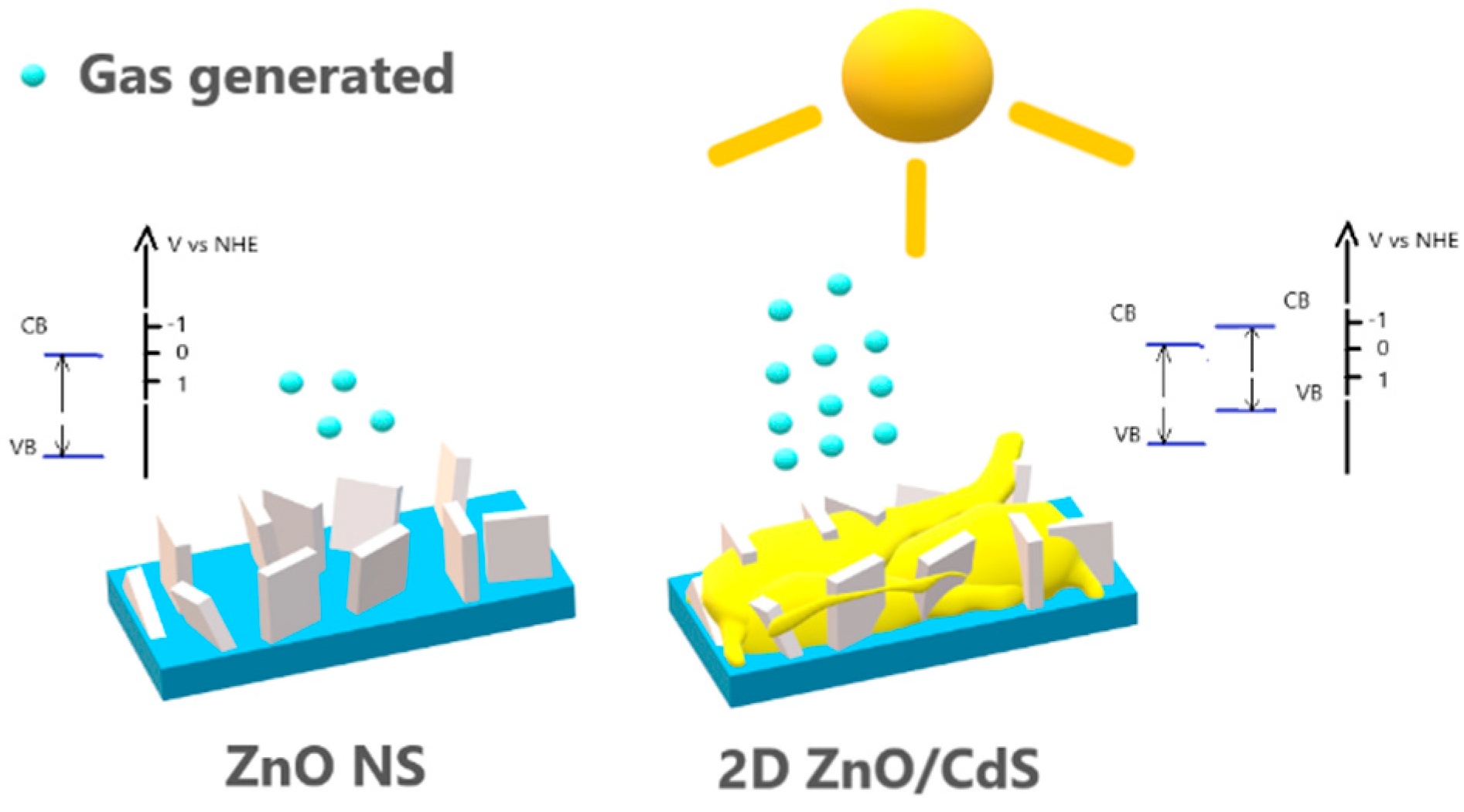
The J of ZnO NS (a) reaches 82 μA/cm2, which is less than the J of ZnO NS (b), which is equal to 98 μA/cm2. Comparing the Nyquist plot for ZnO NS (a) and ZnO NS (b) (see Figure 7b black and red semicircles, respectively) reveals that a larger surface area of ZnO NS (b) leads to improved charge transfer performance between the photoanode and the electrolyte (small radius of semicircle). Figure 6a, blue and purple curves, shows the values of the J recorded during PEC processes for ZnO/CdS (50) and ZnO/CdS (10), respectively. It is seen that a thin layer of CdS in the ZnO/CdS core/shell structure exhibit a higher level of J = 418 μA/cm2. Covering the ZnO NS arrays uniformly by 50 layers of CdS leads to the suppression of J in the PEC cell. Consequently, thin layers of CdS increase the photoelectrochemical efficiency of ZnO/CdS composites. This is in good agreement with photocatalytic activity for MB degradation. The schematic diagram in Figure 8 shows the hierarchy of the band structures of the ZnO/CdS composite, giving a superficial representation of the photocatalysis process on semiconductor photoanodes made in a composite architecture.
Based on the results of this work, it can be assumed that the water treatment or production of pure hydrogen is permissible using elements common in the earth’s crust. This will avoid the widespread use of rare and expensive materials, which will reduce the cost of the final product.
4. Conclusions
The exploitation of oriented and close-packed structures of ZnO NS (Figure 3b) exhibits a greater photoresponse in comparison with a similar structure, the packing of which is less dense (Figure 3a). Accordingly, it is important to control the morphology of the resulting photoactive material. The use of a simple but reliable technique of electrochemical synthesis allows the creation of fine control of the surface and structure of the synthesized sample. Modification of wide-gap semiconductors with narrow-gap semiconductors is one way of creating nanocomposites and heterostructures. It requires the use of several hierarchical synthesis techniques to impart the desired architecture. In this work, using a sequential combination of electrochemical synthesis and the SILAR method, a photoactive nanocomposite with a specified and controlled 2D ZnO/CdS architecture was synthesized. The obtained ZnO/CdS NS photoanode exhibited improved absorption of light and a decrease in the level of exciton recombination, which led to increased photocurrent density up to J = 418 μA/cm2 at 0 V bias vs. Ag/AgCl.
Author Contributions
Conceptualization, N.B.; methodology, D.B.; formal analysis, N.B.; investigation, B.S.; resources, N.B.; data curation, B.S.; writing—original draft preparation, D.B.; writing—review and editing, N.B.; visualization, B.S. All authors have read and agreed to the published version of the manuscript.
Funding
This research was funded by the Ministry of Science and Higher Education of the Republic of Kazakhstan, grant number AP08052381.
Institutional Review Board Statement
Not applicable.
Informed Consent Statement
Not applicable.
Conflicts of Interest
The authors declare no conflict of interest.
References
- Volta, P.; Jeppesen, E. Impacts of Human Activities and Climate Change on Freshwater Fish. Water 2021, 13, 3068. [Google Scholar] [CrossRef]
- Fujishima, A. Electrochemical evidence for the mechanism of the primary stage of photosynthesis. In Book Electrochemical Evidence for the Mechanism of the Primary Stage of Photosynthesis; EditorBulletin of the Chemical Society of Japan: Tokyo, Japan, 1971; pp. 1148–1150. [Google Scholar]
- Shabdan, Y.; Markhabayeva, A.; Bakrano, N.; Nuraje, N. Photoactive Tungsten-Oxide Nanomaterials for Water-Splitting. Nanomaterials 2020, 10, 1871. [Google Scholar] [CrossRef] [PubMed]
- Markhabayeva, A.A.; Moniruddin, M.; Dupre, R.; Abdullin, K.A.; Nuraje, N. Designing of WO3@Co3O4 Heterostructures to Enhance Photoelectrochemical Performances. J. Phys. Chem. A 2020, 124, 486–491. [Google Scholar] [CrossRef] [PubMed]
- Janotti, A.; Van de Walle, C.G. Fundamentals of zinc oxide as a semiconductor. Rep. Prog. Phys. 2009, 72, 12. [Google Scholar] [CrossRef] [Green Version]
- Sharma, V.; Shukla, R.K.; Saxena, N.; Parmar, D.; Das, M.; Dhawan, A. DNA damaging potential of zinc oxide nanoparticles in human epidermal cells. Toxicol. Lett. 2009, 185, 211–218. [Google Scholar] [CrossRef]
- Gupta, T.K. Application of zinc-oxide varistors. J. Am. Ceram. Soc. 1990, 73, 1817–1840. [Google Scholar] [CrossRef]
- Nanto, H.; Minami, T.; Takata, S. Zinc-oxide thin-film ammonia gas sensors with high-sensitivity and excellent selectivity. J. Appl. Phys. 1986, 60, 482–484. [Google Scholar] [CrossRef]
- Becheri, A.; Durr, M.; Lo Nostro, P.; Baglioni, P. Synthesis and characterization of zinc oxide nanoparticles: Application to textiles as UV-absorbers. J. Nanopart. Res. 2008, 10, 679–689. [Google Scholar] [CrossRef]
- Xie, Y.P.; He, Y.P.; Irwin, P.L.; Jin, T.; Shi, X.M. Antibacterial Activity and Mechanism of Action of Zinc Oxide Nanoparticles against Campylobacter jejuni. Appl. Environ. Microbiol. 2011, 77, 2325–2331. [Google Scholar] [CrossRef] [Green Version]
- Goux, A.; Pauporte, T.; Chivot, J.; Lincot, D. Temperature effects on ZnO electrodeposition. Electrochim. Acta 2005, 50, 2239–2248. [Google Scholar] [CrossRef]
- Xu, F.; Lu, Y.N.; Xie, Y.; Liu, Y.F. Controllable morphology evolution of electrodeposited ZnO nano/micro-scale structures in aqueous solution. Mater. Des. 2009, 30, 1704–1711. [Google Scholar] [CrossRef]
- Yin, Y.; Jin, Z.; Hou, F. Enhanced solar water-splitting efficiency using core/sheath heterostructure CdS/TiO(2) nanotube arrays. Nanotechnology 2007, 18, 49. [Google Scholar] [CrossRef] [PubMed]
- Li, C.L.; Yuan, J.A.; Han, B.Y.; Jiang, L.; Shangguan, W.F. TiO2 nanotubes incorporated with CdS for photocatalytic hydrogen production from splitting water under visible light irradiation. Int. J. Hydrogen Energy 2010, 35, 7073–7079. [Google Scholar] [CrossRef]
- Ahmad, H.; Kamarudin, S.K.; Minggu, L.J.; Kassim, M. Hydrogen from photo-catalytic water splitting process: A review. Renew. Sustain. Energy Rev. 2015, 43, 599–610. [Google Scholar] [CrossRef]
- Sadtler, B.; Demchenko, D.O.; Zheng, H.; Hughes, S.M.; Merkle, M.G.; Dahmen, U.; Wang, L.W.; Alivisatos, A.P. Selective Facet Reactivity during Cation Exchange in Cadmium Sulfide Nanorods. J. Am. Chem. Soc. 2009, 131, 5285–5293. [Google Scholar] [CrossRef] [PubMed] [Green Version]
- Xu, Y.; Zhao, W.; Xu, R.; Shi, Y.; Zhang, B. Synthesis of ultrathin CdS nanosheets as efficient visible-light-driven water splitting photocatalysts for hydrogen evolution. Chem. Commun. 2013, 49, 9803–9805. [Google Scholar] [CrossRef] [PubMed]
- Sweeney, R.Y.; Mao, C.B.; Gao, X.X.; Burt, J.L.; Belcher, A.M.; Georgiou, G.; Iverson, B.L. Bacterial biosynthesis of cadmium sulfide nanocrystals. Chem. Biol. 2004, 11, 1553–1559. [Google Scholar] [CrossRef] [PubMed] [Green Version]
- Mews, A.; Eychmuller, A.; Giersig, M.; Schooss, D.; Weller, H. Preparation, characterization, and photophysics of the quantum-dot quantum-well system CdS/HgS/CdS. J. Phys. Chem. 1994, 98, 934–941. [Google Scholar] [CrossRef]
- Shangguan, W.F.; Yoshida, A. Photocatalytic hydrogen evolution from water on nanocomposites incorporating cadmium sulfide into the interlayer. J. Phys. Chem. B 2002, 106, 12227–12230. [Google Scholar] [CrossRef]
- Xu, J.; Cao, X.J. Characterization and mechanism of MoS2/CdS composite photocatalyst used for hydrogen production from water splitting under visible light. Chem. Eng. J. 2015, 260, 642–648. [Google Scholar] [CrossRef]
- Sathish, M.; Viswanathan, B.; Viswanath, R.P. Alternate synthetic strategy for the preparation of CdS nanoparticles and its exploitation for water splitting. Int. J. Hydrogen Energy 2006, 31, 891–898. [Google Scholar] [CrossRef]
- Henglein, A. Photo-degradation and fluorescence of colloidal-cadmium sulfide in aqueous-solution. Ber. Bunsen-Ges.-Phys. Chem. Chem. Phys. 1982, 86, 301–305. [Google Scholar] [CrossRef]
- Ding, L.; Zhou, H.; Lou, S.; Ding, J.; Zhang, D.; Zhu, H.X.; Fan, T.X. Butterfly wing architecture assisted CdS/Au/TiO2 Z-scheme type photocatalytic water splitting. Int. J. Hydrogen Energy 2013, 38, 8244–8253. [Google Scholar] [CrossRef]
- Matsumura, M.; Furukawa, S.; Saho, Y.; Tsubomura, H. Cadmium-sulfide photocatalyzed hydrogen-production from aqueous-solutions of sulfite—Effect of crystal-structure and preparation method of the catalyst. J. Phys. Chem. 1985, 89, 1327–1329. [Google Scholar] [CrossRef]
- Johnson, J.; Bakrano, N.; Moniruddin, M.; Iskako, R.; Kudaibergeno, S.; Nuraje, N. Spontaneous polarization field-enhanced charge separation for an iron oxide photo-catalyst. N. J. Chem. 2017, 41, 15528–15532. [Google Scholar] [CrossRef]
- Tak, Y.; Hong, S.J.; Lee, J.S.; Yong, K. Fabrication of ZnO/CdS core/shell nanowire arrays for efficient solar energy conversion. J. Mater. Chem. 2009, 19, 5945–5951. [Google Scholar] [CrossRef] [Green Version]
- Kudaibergeno, S.; Tatykhanova, G.; Bakrano, N.; Tursunova, R. Layer-by-Layer Thin Films and Coatings Containing Metal Nanoparticles in Catalysis. In Thin Film Processes—Artifacts on Surface Phenomena and Technological Facets; Thirumalai, J., Ed.; IntechOpen: London, UK, 2017. [Google Scholar]
- Fang, Y.L.; Li, Z.Y.; Xu, S.; Han, D.D.; Lu, D.Y. Optical properties and photocatalytic activities of spherical ZnO and flower-like ZnO structures synthesized by facile hydrothermal method. J. Alloys Compd. 2013, 575, 359–363. [Google Scholar] [CrossRef]
- Fu, H.B.; Xu, T.G.; Zhu, S.B.; Zhu, Y.F. Photocorrosion Inhibition and Enhancement of Photocatalytic Activity for ZnO via Hybridization with C-60. Environ. Sci. Technol. 2008, 42, 8064–8069. [Google Scholar] [CrossRef]
- Jawale, D.; Al-fahdawi, A.; Salve, S.; Pandit, S.; Dawange, G.; Gugale, G.; Chaskar, M.; Hammiche, D.; Arbuj, S. Pandit 6, 13-pentacenequinone/zinc oxide nanocomposites for organic dye degradation. Mater. Today-Proc. 2022, 52, 17–20. [Google Scholar] [CrossRef]
Figure 1.
Schematic representation of 1 cycle of SILAR technic.
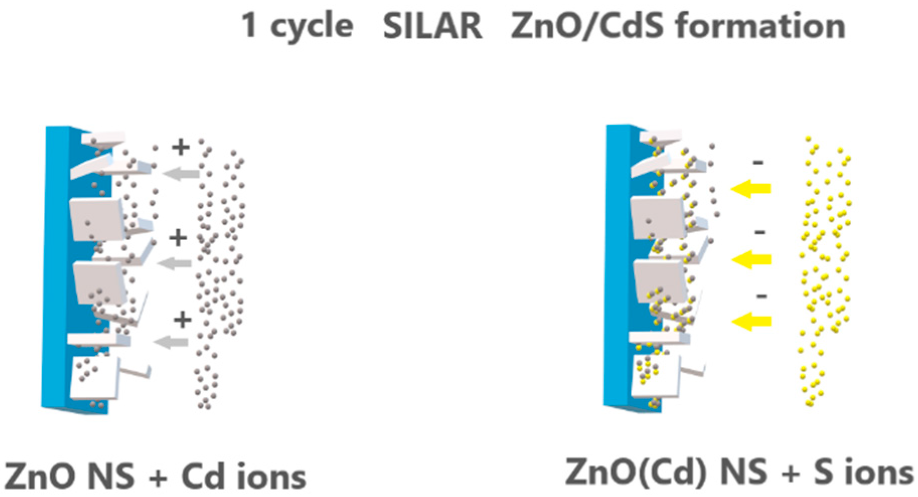
Figure 2.
XRD pattern of ZnO/CdS nanocomposites and ZnO NS (a) main and insert, respectively.
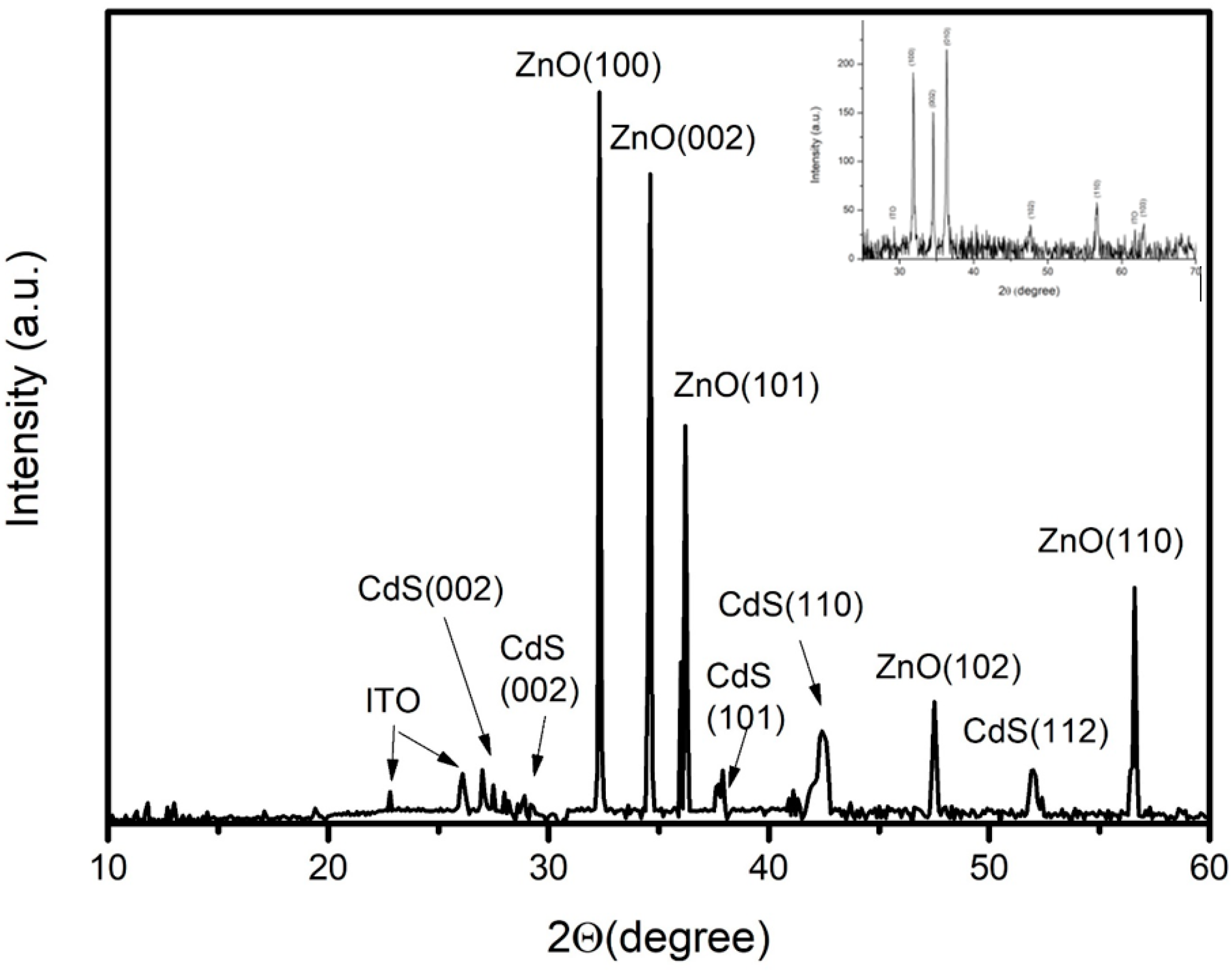
Figure 3.
SEM image of the surface morphology of 2D ZnO obtained by electrochemical synthesis at a concentration of (a) 0.01 M Zn ions, (b) and (c) 0.5 M Zn ions.
Figure 3.
SEM image of the surface morphology of 2D ZnO obtained by electrochemical synthesis at a concentration of (a) 0.01 M Zn ions, (b) and (c) 0.5 M Zn ions.
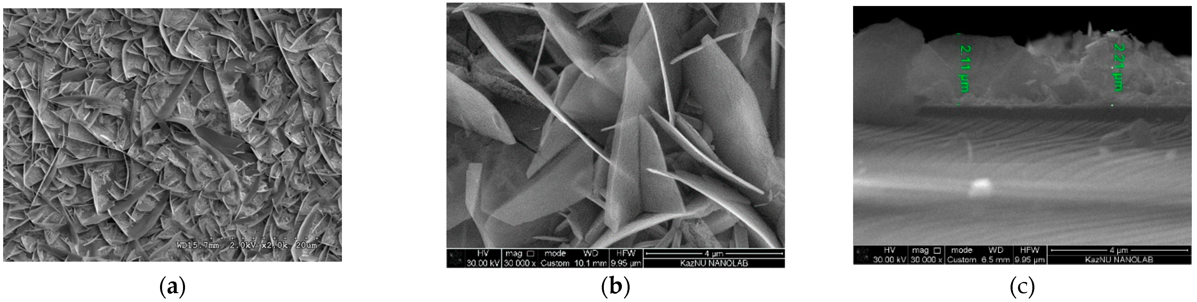
Figure 4.
Optical properties. (a) UV/vis absorption of ZnO NS and ZnO/CdS nanocomposites; (b) PL spectrum of ZnO NS.
Figure 4.
Optical properties. (a) UV/vis absorption of ZnO NS and ZnO/CdS nanocomposites; (b) PL spectrum of ZnO NS.
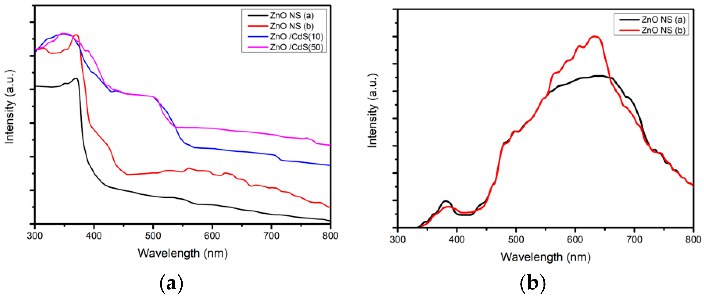
Figure 5.
SEM micrograph of ZnO/CdS composite. (a) 10 cycles; (b) 50 cycles.
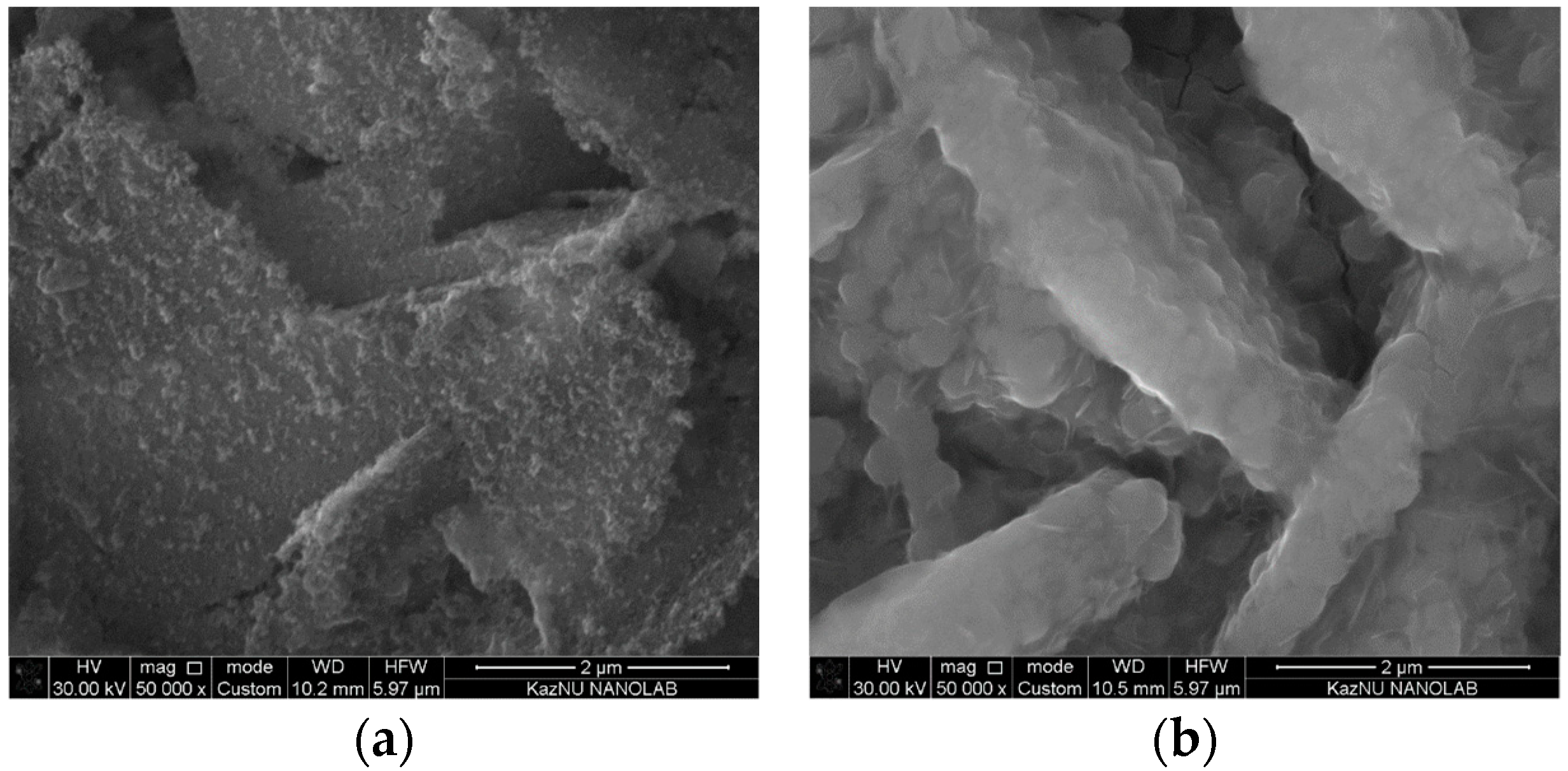
Figure 6.
Photodegradation/adsorption graphs: (a) adsorption analyses in-dark; (b) under UV-vis irradiation.
Figure 6.
Photodegradation/adsorption graphs: (a) adsorption analyses in-dark; (b) under UV-vis irradiation.
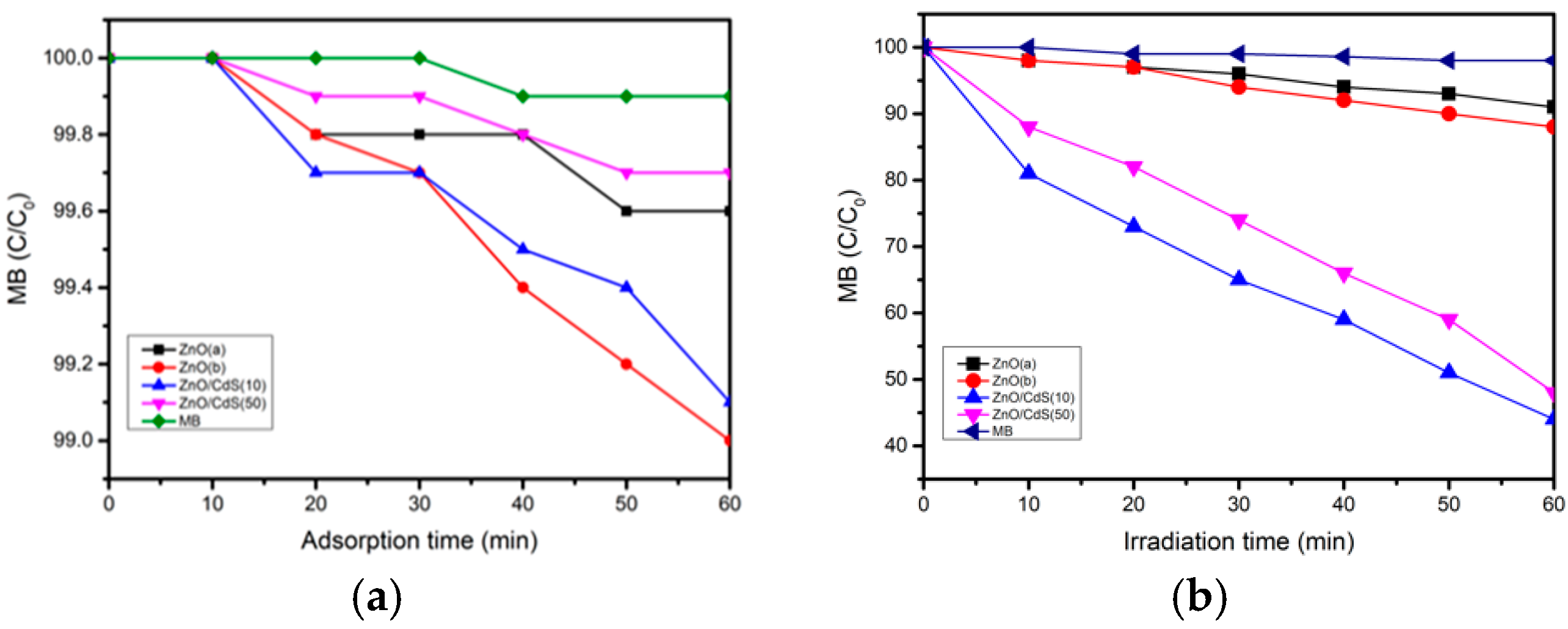
Figure 7.
(a) J-t curves; (b) Nyquist plot at 0 V Ag/AgCl.

Figure 8.
Schematic diagram of the photocatalysis process of ZnO NS (left) and ZnO/CdS nanocomposites (right).
Figure 8.
Schematic diagram of the photocatalysis process of ZnO NS (left) and ZnO/CdS nanocomposites (right).
Publisher’s Note: MDPI stays neutral with regard to jurisdictional claims in published maps and institutional affiliations. |
© 2022 by the authors. Licensee MDPI, Basel, Switzerland. This article is an open access article distributed under the terms and conditions of the Creative Commons Attribution (CC BY) license (https://creativecommons.org/licenses/by/4.0/).
Share and Cite
MDPI and ACS Style
Bakranova, D.; Seitov, B.; Bakranov, N. Preparation and Photocatalytic/Photoelectrochemical Investigation of 2D ZnO/CdS Nanocomposites. ChemEngineering 2022, 6, 87. https://doi.org/10.3390/chemengineering6060087
AMA Style
Bakranova D, Seitov B, Bakranov N. Preparation and Photocatalytic/Photoelectrochemical Investigation of 2D ZnO/CdS Nanocomposites. ChemEngineering. 2022; 6(6):87. https://doi.org/10.3390/chemengineering6060087
Chicago/Turabian StyleBakranova, Dina, Bekbolat Seitov, and Nurlan Bakranov. 2022. "Preparation and Photocatalytic/Photoelectrochemical Investigation of 2D ZnO/CdS Nanocomposites" ChemEngineering 6, no. 6: 87. https://doi.org/10.3390/chemengineering6060087