Communication

Preparation of an Integrated Polarization Navigation Sensor via a Nanoimprint Photolithography Process

1
Key Laboratory of Precision and Non-Traditional Machining Technology of Ministry of Education, Dalian University of Technology, Dalian 116024, China
2
Key Laboratory of Micro/Nano Technology and System of Liaoning Province, Dalian University of Technology, Dalian 116024, China
*
Author to whom correspondence should be addressed.
Photonics 2022, 9(11), 806; https://doi.org/10.3390/photonics9110806
Submission received: 16 September 2022 / Revised: 19 October 2022 / Accepted: 21 October 2022 / Published: 27 October 2022
(This article belongs to the Special Issue Advanced Polarimetry and Polarimetric Imaging)

Abstract

:
Based on the navigation strategy of insects utilizing the polarized skylight, an integrated polarization sensor for autonomous navigation is presented. The polarization sensor is fabricated using the proposed nanoimprint photolithography (NIPL) process by integrating a nanograting polarizer and an image chip. The NIPL process uses a UV-transparent variant template with nanoscale patterns and a microscale metal light-blocking layer. During the NIPL process, part of the resist material is pressed to fill into the nanofeatures of the variant template and is cured under UV exposure. At the same time, the other parts of the resist material create micropatterns according to the light-blocking layer. Polymer-based variant templates can be used for conformal contacts on non-flat substrates with excellent pattern transfer fidelity. The NIPL process is suitable for cross-scale micro–nano fabrication in wide applications. The measurement error of the polarization angle of the integrated polarization sensor is ±0.2°; thus, it will have a good application prospect in the polarization navigation application.

1. Introduction

Navigation technique is an essential ability to survive and develop for human beings and becomes increasingly important in a wide range of applications in both military and civil fields [1,2]. Consequent to several billion years of evolution, many animals, especially insects, have formed ingenious navigational capabilities. Some of them are sensitive to the polarization of light and utilize polarization information for communication and navigation [3,4,5,6]. The bionic polarization navigation inspired by the biological celestial polarization orientation method has advantages such as autonomy, immunity to interference, and no error accumulation [7]. Biomimetic navigation devices based on the polarization of the skylight have been developed [8,9,10,11,12]. Compared with photodiode-based polarization sensors, image-based polarization sensors are less susceptible to the surrounding environment, occlusion, or other external factors. In our previous paper [10], a multidirectional nanowire grid polarizer was integrated into a complementary metal oxide semiconductor (CMOS) sensor through nanoimprint lithography. A gap exists between the nanowire polarizer and the image plane due to the glass package cover of the CMOS sensor, and the level of integration has further room for improvement.
With respect to the integration of the nanowire polarizer and the image chip, it involves a micro–nano cross-scale process for the nanowires and other patterns such as the electrodes of the image chip. Among the fabrication techniques of micro- and nanoscale-integrated structures, the multistep shaping method [13,14,15] combines the commonly used microprocesses such as MEMS with nanofabrication technology to perform multiple pattern transfers on the same substrate, and finally, the micro- and nanoscale-integrated structures are obtained. It is flexible and can realize multiscale-integrated structures with complex patterns. However, the multistep shaping method usually requires multiple “lithography–etching” processes to process patterns for different sizes, in which the steps need to be precisely aligned with each other, and the accuracy of pattern transfer is easily reduced, resulting in a complex, time-consuming, and costly process. As commonly used nanofabrication techniques, electron-beam lithography (EBL) and focused ion beam (FIB) have high resolution but costly equipment and low efficiency and, therefore, are especially not suitable for micronlevel or larger patterns [16,17]. Nanoimprint lithography (NIL) is highly adaptable in both research and industry because of its high throughput and low cost, which can prepare micro- and nanostructures on large areas with high efficiency [18,19,20,21]. NIL replicates nanostructures on a template onto a polymer film by driving polymer flow through mechanical extrusion. With a core of polymer flow, NIL thus has some potential deficiency; for example, the amount of polymer flow required is different for different sizes of feature structures at different locations, and larger structure features on the template will require more polymer flow transferred at a far distance. Filling efficiency is different, and pattern replication may result in pattern defects or incomplete pattern filling. This problem is more obvious when producing cross-scale structures with non-uniform distributions. Such limitations of NIL are inherent and are related to the fabricated patterns, which cannot be solved by methods such as optimizing the process parameters of nanoimprinting technology. To enable the fabrication of micro–nano cross-scale structures, especially when it comes to the fabrication of large-area structures, NIL needs to break through its limitations. In addition, the lithography process is the most central bottleneck process in the micro- and nanomanufacturing industries such as integrated circuit manufacturing. In addition to the further development of new lithography techniques suitable for smaller patterns, improving the accuracy and flexibility of the existing lithography process is also of extraordinary significance for micro- and nanodevice fabrication. Some methods based on nanoimprinting and standard photolithography are reported. Cheng et al. proposed the combined nanoimprint and photolithography (CNP) using the hybrid mask–mold (HMM) and with the CNP method, resist patterns with a higher aspect ratio and with no residual layer can be obtained in a single step [22]. The utilized HMM was made from fused silica by appropriate lithography and RIE process. Christiansen et al. demonstrated the fabrication of polymer optics with nm to mm features by CNP [23,24]. The CNP stamp was fabricated through EBL on a quartz wafer. Lohse et al. demonstrated a scalable method via CNP for the preparation of microfluidic channels with nanopatterns. The excellent compatibilities of the polymer master to the UV-PDMS stamp and further between the UV-PDMS stamp and the imprint resist mr-NIL are the key factors for replication on large scale with high accuracy [25].
This paper demonstrates a nanoimprint photolithography (NIPL) process that integrates conventional optical lithography into nanoimprint lithography, sharing the advantages and compensating for each other’s limitations, using the mechanical deformation mechanism of nanoimprinting to replicate nanoscale patterns and the selective curing mechanism of optical lithography to make micronscale patterns, by a freely definable micro–nano variant template. The variant template is made from a common UV transparent soft stamp via the T-NIL and lift-off process, which can achieve conformal contacts on non-flat substrates with excellent pattern transfer fidelity. Through the NIPL process, the polarization navigation sensor is fabricated by integrating an image chip with a multiorientation nanowire polarizer. Finally, a performance test is implemented, and the measurement results are presented.

2. Nanoimprint Photolithography (NIPL) Process for Micro–Nano Cross-Scale Integration Process

Depending on the curing principle of the utilized resist, NIL can be divided into thermal NIL (T-NIL) and UV NIL, with the use of thermally or UV-cured resist, respectively. For the UV NIL process [26], when exposed to UV light, the small molecules of the resist polymer undergo photochemical reactions to form macromolecular networks, with a dramatic increase in mechanical strength and thermal and chemical stability, which are not easily soluble. Some photolithography negative resists also have similar photochemical reaction characteristics, such as SU-8 photoresist, so these photosensitive photolithography negative resists can be used in the UV NIL. Another similarity between UV NIL and conventional optical lithography is that the required templates in both are made of UV-transparent materials. While the masks commonly used in conventional optical lithography are graphite printed on a PET film or chromium deposited on glass, the molds commonly used in the UV NIL are quartz glass or polymeric soft molds. Quartz glass mold is hard and brittle and tends to exert permanent damage such as fractures when in use. A flexible polymer mold, by contrast, can avoid damages, where the pattern of the master mold is first copied 1:1 to the polymer mold and then transferred to the polymer film. The polymer mold not only avoids the “hard–hard” contact between the master mold and the substrate, thus prolonging the service life of the expensive master mold, but also ensures high fidelity by conformal contacts on uneven substrates due to the flexible characteristics of the soft mold, which extends the application of NIL for complex functional devices. In this paper, a nanoimprint photolithography (NIPL) process is proposed based on the respective characteristics of UV NIL and photolithography, correlating the similarities between them by using a UV-curable, imprinting resist material and a freely definable micro–nano variant template according to the requirements. A cross-scale micro–nano-integrated fabrication is realized.

2.1. Fabrication of the Variant Template

Variant templates are made of UV-transparent polymer films that include nanoscale surface structures as well as larger metal light-blocking layers that can be used as both imprint molds for defining nanopatterns and lithographic masks for defining the patterns at the micronscale and larger. The nanoscale features of the variant template are fabricated via the T-NIL process, followed by deposition and lift-off processes to fabricate the light-blocking layers on the variant template as a lithographic mask. The variant templates can be made from the same NIL master mold to apply in different applications, and the light-blocking layer of the variant template can be designed according to the application requirements using conventional MEMS processes, which greatly enhances the flexibility and adaptability of the NIPL process and dispenses with the needs for additional expensive equipment.
The process flow of fabricating the variant template is shown in Figure 1.
Firstly, the nanostructures of the variant template are replicated from the master mold (generally silicon or nickel mold) using T-NIL (Figure 1a). The parameters for the T-NIL are shown in Figure 1e. The soft mold is placed on top of the master mold with sufficient surface contact to remove the air bubbles between the soft mold and the master mold. The imprinting temperature is generally up to 20–50 °C above the glass transition temperature (Tg) of the polymer mold, and therefore the polymer mold has good fluidity. High temperature and high pressure are maintained for a period to ensure the polymer mold sufficiently flows and fills into the concave structure of the master mold. Subsequently, the temperature is reduced to the demolding temperature, which is generally 20–40 °C below the Tg of the polymer mold.
Secondly, the metal film is deposited as a light-blocking layer with the desired micropattern in combination with optical lithography (Figure 1b,c).
Finally, after the lift-off process, the variant template is obtained with the nanoscale patterns and micronscale light-blocking layer (Figure 1d).

2.2. NIPL Process

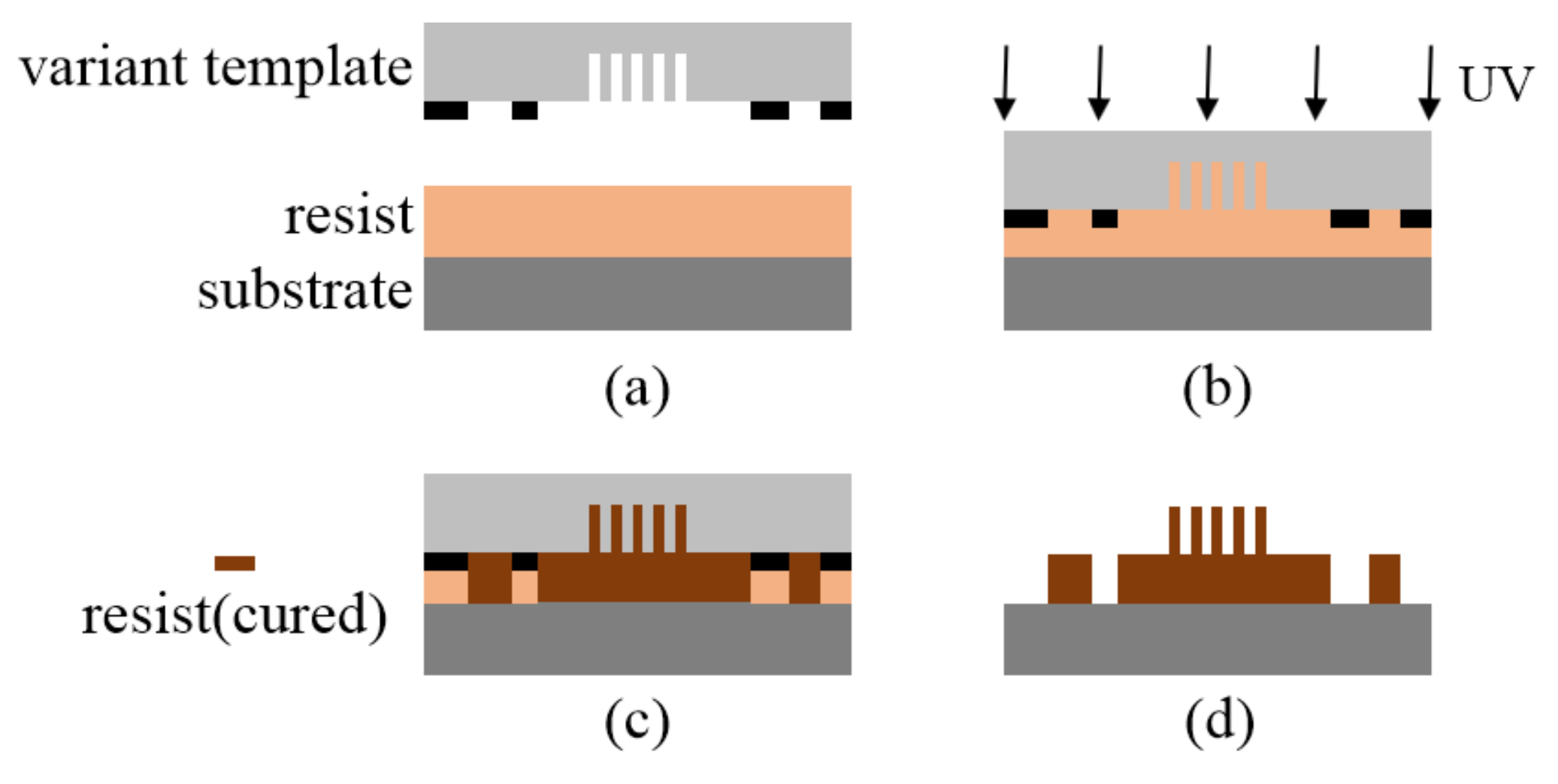
The steps of the NIPL process are very simple, as shown in Figure 2. The variant template is first pressed into the resist film while being UV-exposed (Figure 2a,b). The part of the resist under UV exposure is cured, and the other part under the metal light-blocking layer remains. After the variant template and substrate are separated, the substrate is immersed in the developing solution to remove the unexposed resist. Both nanoscale and larger-scale patterns can be produced in the resist film in one single step. The NIPL process requires no additional equipment and can be performed with existing NIL machines; it can produce complex, cross-scale structures including nanoscale patterns in a single step without the need for multiple alignments and lithography processes, and the production accuracy is comparable to that of conventional NIL.

3. Polarization Navigation Sensor with the Integration of Multidirectional Nanogratings and the Image Chip

3.1. Integrated Fabrication of Multidirectional Nanogratings and the Image Chip

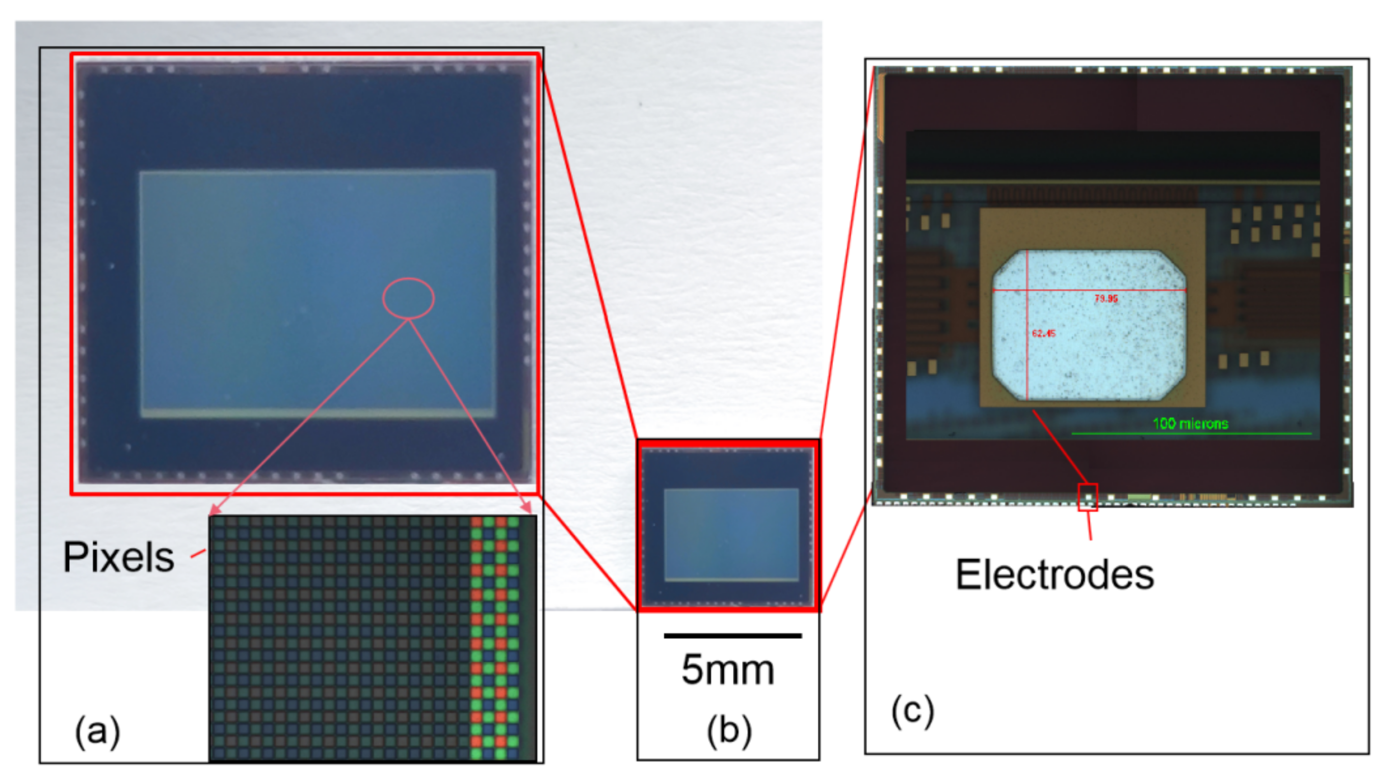
The area of the image chip is 6300 um × 5748 um, with 55 pin electrodes distributed around the edges, and the electrode size is 80 um × 63 um. The effective pixel array of the image chip is 732(H) × 492(V), with a pixel area of 6.5 um × 6.5 um, and the effective image area is 4760 um × 3200 um, shown as “Pixels” in Figure 3.
In the integrated fabrication process, two key issues need to be solved: (1) nanogratings should be integrated into the pixel area of the image chip; (2) to ensure that the edge-pin electrodes of the image chip can be connected to the external data acquisition processing circuit, the metal layer of the chip electrodes should be kept intact and undamaged, and the electrode surface should be clean and kept free from contamination by reagents such as the photoresist material during the integration process; both of these factors need to be considered.
For the integration process, the conventional process is first to fabricate the nanogratings on the pixel area via EBL, NIL, or other nanotechnology; subsequently, the metal film is deposited to form a metal nanowire polarizer, and the premise is that the electrodes are covered by the resist film to avoid short circuit to each other; finally, the residual resist and metal films on the electrodes are removed through, for example, dry etching or RIE. The conventional process is complicated and particularly difficult due to the edge bead effect. The edge bead effect is inevitable when coating the resist due to the flow characteristics of the resist, which leads to a thicker resist film at the edge of the substrate. Small-size substrates and non-circular substrates will aggravate the edge bead phenomenon [27]. When using full-chip-exposed lithography techniques such as UV NIL, the inhomogeneity of the resist film thickness can cause the over-etching of the pattern at the center or under-etching at the edges. To reduce the effect of edge beads, one of the common methods is chemical edge bead removal, which employs a chemical solvent dispensed on the edge of the substrate through a nozzle to eliminate the accumulated resist material on the substrate edge [28,29,30]. Other approaches, such as covering the edge of the substrate with heat-resistant tape, using a polymer holder to increase the planarity of the photoresist film, using a bell-shaped cover to minimize air turbulence while rotating, and the constant volume injection method, have been reported [31,32,33,34].
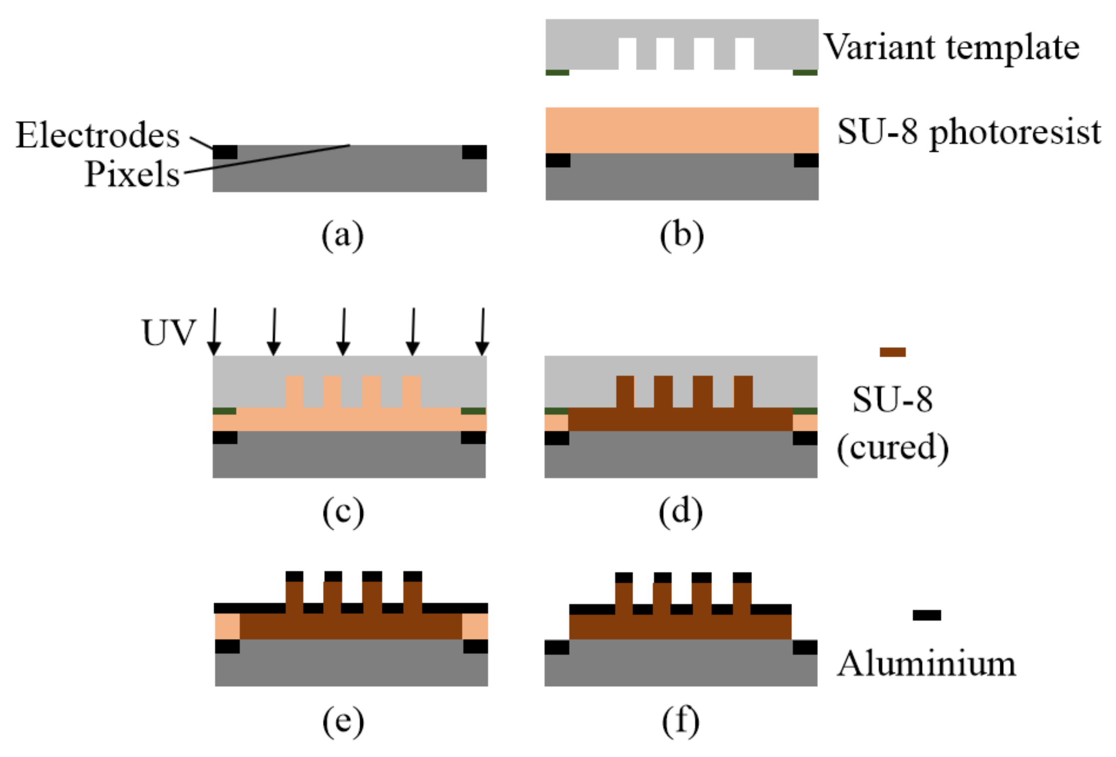
In this paper, NIPL is used to integrate the nanogratings and the image chip. With the proper variant template, nanogratings can be fabricated on the pixels, while the electrodes at the edges can remain clean and intact (Figure 4).
Firstly, the image chip is cleaned to remove dust and organic pollutants. The image chip is immersed in acetone in a water bath (90 °C) for 10 min, followed by ultrasonic cleaning for 10 min with residual heat. The chip is moved into anhydrous ethanol, similar to the previous step, in a water bath (90 °C) for 10 min and ultrasonic cleaning for 10 min. After rinsing with deionized water, the image chip is ultrasonically cleaned in deionized water for 10 min and put into an oven to dry.
Secondly, SU-8 2015 is mixed with a diluent SU-8 2000 thinner at a ratio of 5:4 and spin-coated on the image chip surface. The spin-coating process begins at a low speed of 500 rpm for 6 s to spread the SU-8 resist evenly on the chip surface. Then, the excess solution is shaken out at the high speed of 4000 rpm for 30 s to make the SU-8 resist film more uniform. The image chip is placed on the horizontal heating plate for prebaking to remove the solvent in the SU-8 resist and to improve the adhesion between the SU-8 resist and the image chip. To eliminate the stress inside the SU-8 resist during spin-coating, the prebaking temperature is stepped up from 65 °C to 95 °C, increasing by 5 °C every 10 min, and remaining at 95 °C for 30 min, and then cooling naturally in air, to room temperature. This stepped changing temperature method can reduce the thermal stress caused by the drastic change in temperature and avoid the defect of SU-8 resist film wrinkle.
Then, the variant template for NIPL is fabricated. IPS soft mold is replicated via the T-NIL method for nanopatterns of the variant template, which contain nanogratings in four directions of 0°, 90°, 60°, and 150°, each with a period of 200 nm, a duty cycle of 0.5 and an area of 1.3 mm × 1.3 mm. The imprint parameters are 4 MPa at 155 °C, and the demolding temperature is 115 °C. Subsequently, the metal light-blocking layer is deposited via the magnetron sputtering process, including a 10 nm chromium (Cr) film layer and a 200 nm nickel (Ni) film layer, successively. The thin Cr film can improve the adhesion of Ni to the IPS soft mold, and the 200 nm Ni film has a UV transmission of about 0. The metal light-blocking layer covers the variant template except for the edges corresponding to the electrodes of the image chip.
Next, the NIPL process is performed using the SU-8 resist with a temperature of 85 °C and pressure of 4 MPa. After UV radiation, the exposed SU-8 resist is cured.
Then, 80 nm of metallic Al is deposited via the thermal vapor deposition process on the chip. Double-layer metal nanogratings are made on the pixel area.
Finally, the chip is immersed into the SU-8 developer to remove the uncured SU-8 resist with the attached Al film. After the SU-8 photoresist is spin-coated on the whole chip, there is a stack at the corners of the chip due to the edge bead effect. The selective local exposure of the NIPL process can leave the photoresist at the edges unexposed to UV, and therefore it can be easily removed using the developer.
As shown in Figure 5, the polarization chip is fabricated by integrating the image chip with multidirectional metal nanogratings, with nanograting directions of 0°, 90°, 60°, and 150°, a period of 200 nm, and a duty cycle of 0.5. The photograph of the integrated polarization sensor is shown in Figure 5a. As shown in Figure 5b, the electrodes are clean and intact after the integrating process. Figure 5c illustrates the SEM images of the multidirectional nanogratings on the test piece of silicon by the same integration process.

3.2. Hardware System of Integrated Polarization Sensor

The output electrical signals of the integrated polarization chip contain polarization information that is positively correlated with the intensity of the incident light. In the control processing module, STM32 is selected as a microcontroller unit (MCU) for the polarization information solution and real-time output. STM32 series microcontrollers have low cost and power consumption and are easy in terms of hardware design and program development, with a maximum operating frequency of 72 MHz, flash memory, and 64 K SRAM memory. The STM32 microcontroller contains an internal RTC clock circuit that enables continuous timing using the ticking timer when an external power supply is available. The sensor data can be read through the serial interface while quickly being transferred to the upper machine through another serial interface. The control processing module also includes EEPROM memory, a crystal oscillator, a decoupling capacitor, a filter capacitor, etc. The EEPROM is used to store the registered configuration of the integrated polarization chip, and the crystal provides the clock required for the STM32 microcontroller to work. The photos of the integrated polarization sensor are shown in Figure 5.

3.3. Calculation of Polarization Angle of the Incident Light

The integrated polarization chip contains four polarization units with nanogratings and covered pixels. The polarization units are sensitive to the polarization angle of 0°, 90°, 60°, and 150°, respectively. In theory, the intensities of the pixels in a polarization unit should be identical under irradiation. The output of a polarization unit is calculated as the mean value of the intensities of its pixels, as shown in the following equation:
p ¯ = 1 X Y y = 1 Y x = 1 X p x , y
where p(x,y) is the original intensity of a pixel, and x and y are the row and column numbers of the pixel in the pixel array. X and Y are the row and column dimensions. p ¯ is the mean value as the output of a polarization unit.
In practice, the variance between the pixels and the non-uniformity of the nanogratings may lead to inequality in pixel intensities in a polarization unit. The intensities of some pixels deviant from the majority of the intensities are labeled as abnormal values, which need to be eliminated to avoid reducing the reliability of the sensor and are determined as follows:
σ = 1 X Y 1 y = 1 Y x = 1 X p x , y p ¯ 2
p x , y p ¯ > 3 σ
where σ is the standard deviation. When the intensity of one pixel satisfies Equation (3), it can be regarded as an abnormal value and be eliminated. The above steps are repeated until there are no abnormal values. After eliminating the abnormal values, the mean intensities of pixels are calculated as the final intensity of a polarization unit. A large number of pixels would be sufficient for the calculation to compensate for unexpected situations such as some pixels breaking down, thus enhancing the robustness of the sensor.
When the sensor is illuminated with polarized light, the outputs of the polarization units can be described by the following equations:
s 1 θ = K I 1 + d cos 2 θ s 2 θ = K I 1 d cos 2 θ s 3 θ = K I 1 + d cos 2 θ 2 π 3 s 4 θ = K I 1 d cos 2 θ 2 π 3
where I is the total intensity, d is the degree of polarization, θ is the polarization angle relative to the reference direction of the sensor, and K is a constant.
To eliminate the effect of the intensity of the incident light, the following calculation is implemented:
t 1 = s 1 θ s 2 θ = 1 + d cos 2 θ 1 d cos 2 θ t 2 = s 3 θ s 4 θ = 1 + d cos 2 θ 2 π 3 1 d cos 2 θ 2 π 3
With further elimination of the effect of the polarization degree, the calculated polarization angle is:
k 1 = t 1 1 t 1 + 1 k 2 = t 2 1 t 2 + 1 θ = 1 2 tan 1 1 3 2 k 2 k 1 + 1

3.4. Performance Testing of the Integrated Polarization Sensor

A performance test of the integrated polarization navigation sensor was conducted on a test platform in the laboratory, as shown in Figure 6. A hollow precise rotary table was placed at the output port of the integrating sphere. A polaroid sheet was fastened on the rotary table. The output light of the integrating sphere was uniform and linearly polarized using the polaroid sheet. The polaroid sheet rotated, which was driven by the rotary table, thus resulting in a change in the polarization angle of the light. The performance of the integrated polarization sensor was evaluated by the accuracy of the measured change in the polarization angle.

4. Results and Discussion

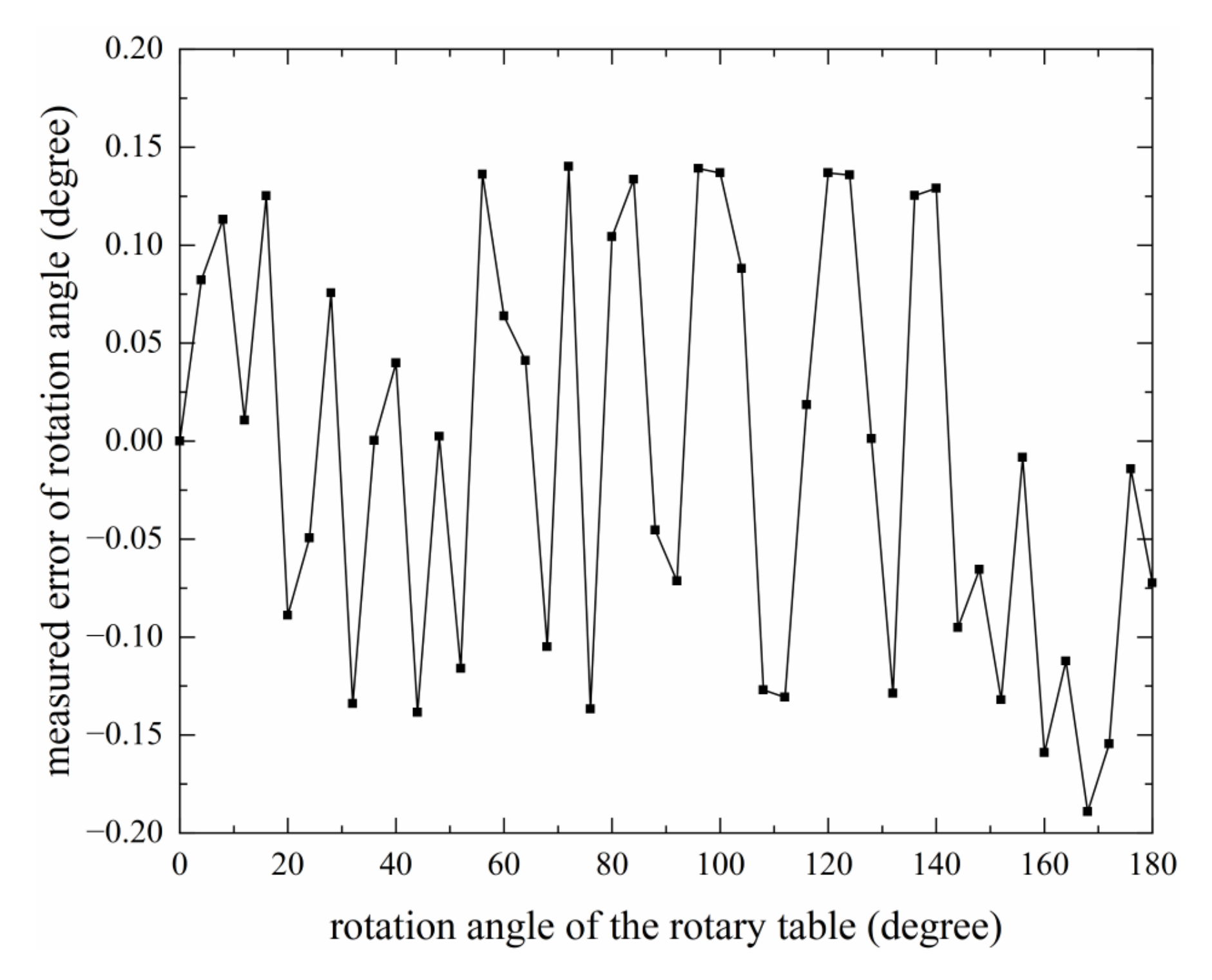
The rotary table stopped every 4° of rotation for a total of 180°. The rotary table remained for 1 min at every stop, and at the same time, the polarization angles of the integrated polarization sensor were calculated. The rotation angle of the rotary table from the starting point was regarded as the theoretical rotation angle. The change in the angle of the sensor between the currently measured angle and the measured angle at the starting point was regarded as the measured rotation angle. The difference between the measured rotation angle and the theoretical rotation angle at every stop was the measured angle error of the polarization sensor. As shown in Figure 7, the error of the measured polarization angle was ±0.2°. The causes of this measurement error are possibly the presence of pixel noise, circuit noise, and the non-uniformity of the nanogratings. Through the performance test, it was shown that the integrated polarization sensor has the capability to detect the polarization angle of incident light. In a further study, we plan to investigate the potential of the integrated polarization sensor for application in autonomous navigation in combination with the distribution of a polarized skylight pattern.

5. Conclusions

This paper presents a nanoimprint photolithography (NIPL) process by combining the respective characteristics of UV NIL and photolithography. In one step, the NIPL process can make cross-scale structures with nanoscale and microscale patterns simultaneously. A polarization chip was fabricated by integrating an image chip with nanogratings using the NIPL process. The polarization angle measurement error of the fabricated polarization navigation sensor was within ±0.2°.
The minimum dimension of the NIPL process demonstrated in this paper was 100 nm, but the limit of dimension for the NIPL process, dependent on the NIL master mold, can be smaller, even down to 10 nm theoretically. The NIPL process is widely applicable to cross-scale integration processes because the utilized variant templates are highly flexible for different application requirements.

Author Contributions

Z.L. conceived the idea of the fabrication of the integrated polarization navigation sensor. Y.F., C.G. and Z.L. performed the experiments. Z.L. analyzed the experimental data and wrote the initial draft of the manuscript. J.C. and R.Z. supervised the project. All authors have read and agreed to the published version of the manuscript.

Funding

This research was funded by the National Natural Science Foundation of China (No. 52175265) and Fundamental Research Funds for the Central Universities (Nos. DUT21ZD101, DUT21GF308).

Institutional Review Board Statement

Not applicable.

Informed Consent Statement

Not applicable.

Data Availability Statement

The study did not report any data.

Conflicts of Interest

The authors declare no conflict of interest. The funders had no role in the design of the study; in the collection, analyses, or interpretation of data; in the writing of the manuscript; or in the decision to publish the results.

References

  1. Shakeri, R.; Al-Garadi, M.A.; Badawy, A.; Mohamed, A.; Khattab, T.; Al-Ali, A.K.; Harras, K.A.; Guizani, M. Design challenges of Multi-UAV systems in Cyber-Physical applications: A comprehensive survey and future directions. IEEE Commun. Surv. Tut. 2019, 21, 3340–3385. [Google Scholar] [CrossRef] [Green Version]
  2. Olikhov, I.; Golchenko, A. Electron-beam-pumped semiconductor laser emitters in glideslope aircraft landing system. Photonics 2013, 4, 76–93. [Google Scholar]
  3. Greif, S.; Borissov, I.; Yovel, Y.; Holland, R.A. A functional role of the sky’s polarization pattern for orientation in the greater mouse-eared bat. Nat. Commun. 2014, 5, 4488. [Google Scholar] [CrossRef] [PubMed] [Green Version]
  4. Hartmann, G.; Wehner, R. The ants path integration system-a neural architecture. Biol. Cybern. 1995, 73, 483–497. [Google Scholar] [CrossRef]
  5. Wehner, R. Desert ant navigation: How miniature brains solve complex tasks. J. Comp. Physiol. A 2003, 189, 579–588. [Google Scholar] [CrossRef] [Green Version]
  6. Froy, O.; Gotter, A.L.; Casselman, A.L.; Reppert, S.M. Illuminating the circadian clock in monarch butterfly migration. Science 2003, 300, 1303–1305. [Google Scholar] [CrossRef]
  7. Powell, S.B.; Garnett, R.; Marshall, J.; Rizk, C.; Gruev, V. Bioinspired polarization vision enables underwater geolocalization. Sci. Adv. 2018, 4, eaao6841. [Google Scholar] [CrossRef] [Green Version]
  8. Lambrinos, D.; Maris, M.; Kobayashi, H.; Labhart, T.; Pfeifer, R.; Wehner, R. An autonomous agent navigating with a polarized light compass. Adapt. Behav. 1997, 6, 131–161. [Google Scholar] [CrossRef]
  9. Chu, J.K.; Wang, Z.W.; Guan, L.; Liu, Z.; Wang, Y.L.; Zhang, R. Integrated polarization dependent photodetector and its application for polarization navigation. IEEE Photonic. Technol. Lett. 2014, 26, 469–472. [Google Scholar]
  10. Liu, Z.; Zhang, R.; Wang, Z.W.; Guan, L.; Li, B.; Chu, J.K. Integrated polarization-dependent sensor for autonomous navigation. J. Micro Nanolith. Mem. 2015, 14, 015001. [Google Scholar] [CrossRef]
  11. Fan, C.; Hu, X.P.; Lian, J.X.; Zhang, L.L.; He, X.F. Design and calibration of a novel Camera-Based Bio-Inspired polarization navigation sensor. IEEE Sens. J. 2016, 16, 3640–3648. [Google Scholar] [CrossRef]
  12. Lu, H.; Zhao, K.C.; Wang, X.C.; You, Z.; Huang, K.L. Real-time imaging orientation determination system to verify imaging polarization navigation algorithm. Sensors 2016, 16, 144. [Google Scholar] [CrossRef] [PubMed]
  13. Bhushan, B.; Jung, Y.C. Natural and biomimetic artificial surfaces for superhydrophobicity, self-cleaning, low adhesion, and drag reduction. Prog. Mater. Sci. 2011, 56, 1–108. [Google Scholar] [CrossRef] [Green Version]
  14. Kim, J.; Bae, W.; Choung, H.; Lim, K.T.; Seonwoo, H.; Jeong, H.E.; Suh, K.; Jeon, N.L.; Choung, P.; Chung, J.H. Multiscale patterned transplantable stem cell patches for bone tissue regeneration. Biomaterials 2014, 35, 9058–9067. [Google Scholar] [CrossRef] [PubMed]
  15. He, Y.; Jiang, C.; Yin, H.; Chen, J.; Yuan, W. Superhydrophobic silicon surfaces with micro-nano hierarchical structures via deep reactive ion etching and galvanic etching. J. Colloid Interf. Sci. 2011, 364, 219–229. [Google Scholar] [CrossRef]
  16. Ruffato, G.; Capaldo, P.; Massari, M.; Mezzadrelli, A.; Romanato, F. Pancharatnam-Berry optical elements for spin and orbital angular momentum division demultiplexing. Photonics 2018, 5, 46. [Google Scholar] [CrossRef] [Green Version]
  17. Munshi, A.H.; Kephart, J.M.; Abbas, A.; Danielson, A.; Gelinas, G.; Beaudry, J.N.; Barth, K.L.; Walls, J.M.; Sampath, W.S. Effect of CdCl2 passivation treatment on microstructure and performance of CdSeTe/CdTe thin-film photovoltaic devices. Sol. Energ. Mat. Sol. C 2018, 186, 259–265. [Google Scholar] [CrossRef] [Green Version]
  18. Toyoda, H.; Kimino, K.; Kawano, A.; Takahara, J. Incandescent Light Bulbs Based on a Refractory Metasurface. Photonics 2019, 6, 105. [Google Scholar] [CrossRef] [Green Version]
  19. Hillmer, H.; Woidt, C.; Kobylinskiy, A.; Kraus, M.; Istock, A.; Iskhandar, M.S.Q.; Brunner, R.; Kusserow, T. Miniaturized interferometric sensors with spectral tunability for optical fiber Technology-A comparison of size requirements, performance, and new concepts. Photonics 2021, 8, 332. [Google Scholar] [CrossRef]
  20. Dundar, A.F.; Kolewe, K.W.; Homyak, B.; Kurtz, I.S.; Schiffman, J.D.; Watkins, J.J. Bioinspired photocatalytic Shark-Skin surfaces with antibacterial and antifouling activity via nanoimprint lithography. ACS Appl. Mater. Interfaces 2018, 10, 20055–20063. [Google Scholar] [CrossRef]
  21. Suresh, V.; Ding, L.; Chew, A.B.; Yap, F.L. Fabrication of Large-Area flexible SERS substrates by nanoimprint lithography. ACS Appl. Nano Mater. 2018, 1, 886–893. [Google Scholar] [CrossRef]
  22. Cheng, X.; Guo, L.J. A combined-nanoimprint-and-photolithography patterning technique. Microelectron. Eng. 2004, 71, 277–282. [Google Scholar] [CrossRef]
  23. Brokner-Christiansen, M.; Scholer, M.; Gersborg-Hansen, M.; Kristensen, A.; IEEE. Combined Nanoimprint and Photolithography of Integrated Polymer Optics. In Proceedings of the IEEE LEOS Summer Topical Meeting 2007, Portland, OR, USA, 23–25 July 2007. [Google Scholar]
  24. Christiansen, M.B.; Scholer, M.; Kristensen, A. Integration of active and passive polymer optics. Opt. Express 2007, 15, 3931–3939. [Google Scholar] [CrossRef]
  25. Lohse, M.; Heinrich, M.; Grutzner, S.; Haase, A.; Ramos, I.; Salado, C.; Thesen, M.W.; Grutzner, G. Versatile fabrication method for multiscale hierarchical structured polymer masters using a combination of photo- and nanoimprint lithography. Micro. Nano. Eng. 2021, 10, 100079. [Google Scholar] [CrossRef]
  26. Haisma, J.; Verheijen, M.; Vandenheuvel, K.; Vandenberg, J. Mold-assisted nanolithography: A process for reliable pattern replication. J. Vac. Sci. Technol. B 1996, 14, 4124–4128. [Google Scholar] [CrossRef]
  27. Nithi, A.; On-Uma, N.; Wutthinan, J.; Sitthisuntorn, S.; Charndet, H.; Amporn, P. Study of optimization condition for spin coating of the photoresist film on rectangular substrate by Taguchi design of an experiment. Songklanakarin J. Sci. Technol. 2009, 31, 331–335. [Google Scholar]
  28. Hun, L.; Kangsun, L.; Byungwook, A.; Jing, X.; Linfeng, X.; Kwang, W.O. A new fabrication process for uniform SU-8 thick photoresist structures by simultaneously removing edge bead and air bubbles. J. Micromech. Microeng. 2011, 21, 125006. [Google Scholar]
  29. Shaw, M.; Nawrocki, D.; Hurditch, R.; Johnson, D. Improving the process capability of SU-8. Microsyst. Technol. 2003, 10, 1–6. [Google Scholar] [CrossRef]
  30. Delgadillo, P.; Gronheid, R.; Thode, C.J.; Wu, H.P.; Cao, Y.; Neisser, M.; Somervell, M.; Nafus, K.; Nealey, P.F. Implementation of a chemo-epitaxy flow for directed self-assembly on 300-mm wafer processing equipment. J. Micro Nanolith. MEMS MOEMS 2012, 11, 31302. [Google Scholar] [CrossRef]
  31. Park, H.W.; Kim, H.J.; Roh, J.H.; Choi, J.K.; Cha, K.R. Simple and Cost-Effective method for edge bead removal by using a taping method. J. Korean Phys. Soc. 2018, 73, 1473–1478. [Google Scholar] [CrossRef]
  32. Lin, C.H.; Lee, G.B.; Chang, B.W.; Chang, G.L. A new fabrication process for ultra-thick microfluidic microstructures utilizing SU-8 photoresist. J. Micromech. Microeng. 2002, 12, 590–597. [Google Scholar] [CrossRef] [Green Version]
  33. Pannek, M.; Dunkel, T.; Schubert, D.W. Effect of a bell-shaped cover in spin coating process on final film thickness. Mater. Res. Innov. 2001, 4, 340–343. [Google Scholar] [CrossRef]
  34. Torino, S.; Bhowmick, S.; Iodice, M.; Casalino, M.; Tufano, V.; Selvaggi, D.; Coppola, G.; Gioffrè, M. Edge beads removal in a photolithography process through a polymer mold. Songklanakarin J. Sci. Technol. 2021, 43, 485–491. [Google Scholar]
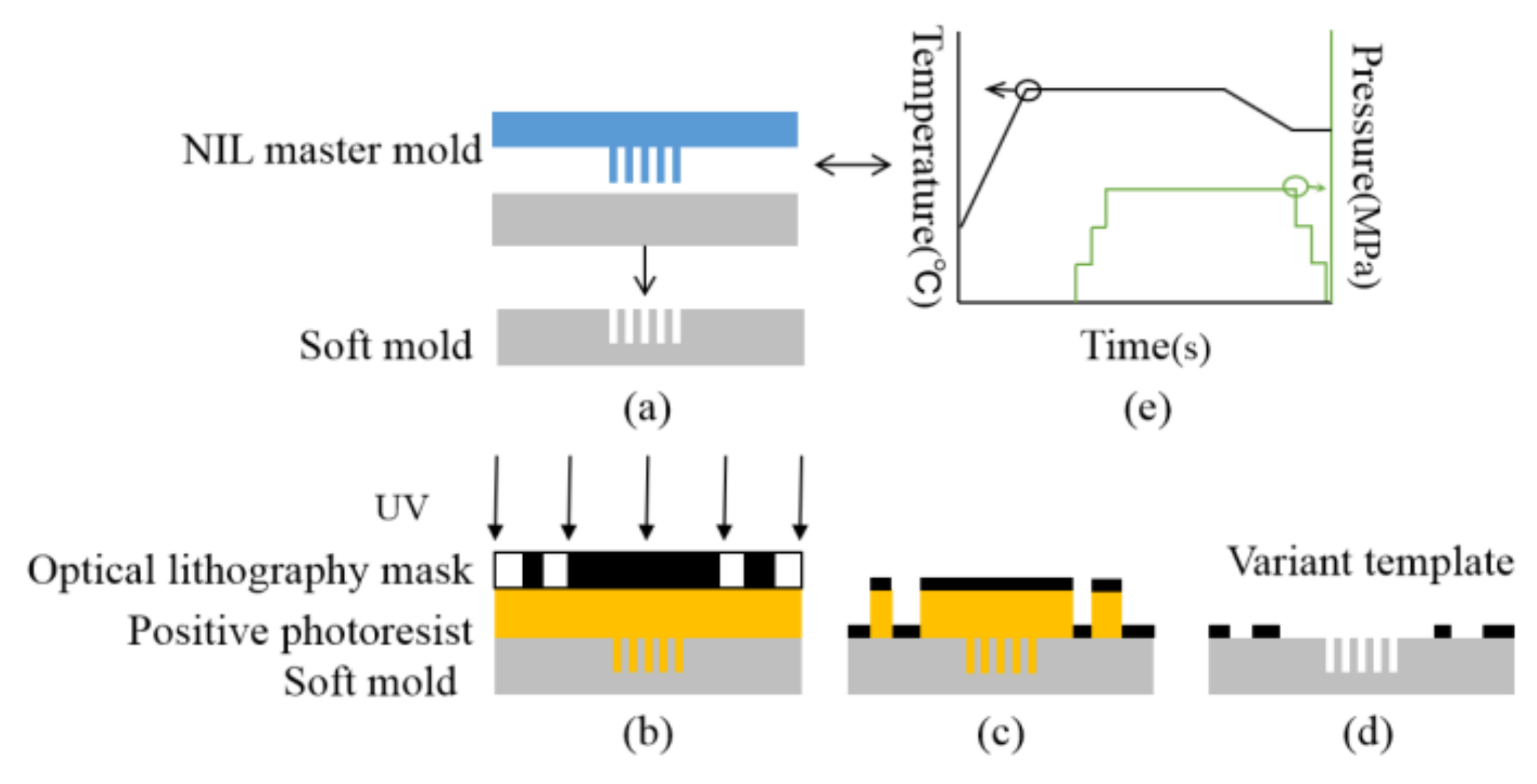
Figure 1. Process flow diagram of variant template fabrication: (a) replication of nanostructures of the variant template by T-NIL; (b) fabrication of micropatterns of the variant template via optical lithography; (c) deposited metal as a light-blocking layer of the variant template; (d) the variant template after lift-off process; (e) parameters for T-NIL.
Photonics 09 00806 g001
Figure 2. NIPL process flow chart: (a) resist is spin-coated on the substrate; (b) UV exposure; (c) cured resist under UV exposure; (d) the cross-scale structures with nano- and larger-scale patterns after demolding and development.
Photonics 09 00806 g002
Figure 3. Optical and microscope photos of the image chip: (a) the photos of the enlarged pixels; (b) the photo of the full image chip; (c) the photos of the enlarged electrodes.
Photonics 09 00806 g003
Figure 4. Integration process based on NIPL process: (a) cleaning the image chip; (b) spin-coating SU-8 photoresist on the image chip; (c,d) NIPL and the exposed SU-8 is cured; (e) metal Al deposited via thermal evaporation process; (f) the residual SU-8 resist and Al film on the electrodes are removed via a lift-off process.
Photonics 09 00806 g004
Figure 5. (a) The photograph of the integrated polarization sensor including the polarization chip, MCU and Power. (b) The photographs of partially enlarged details of nanogratings and adjacent electrodes of the polarization chip (red and blue boxes) in (a). (c) SEM images of multidirectional nanogratings on the test piece of silicon by the same integration process.
Photonics 09 00806 g005
Figure 6. Measurement setup for polarization performance of the sensor.
Photonics 09 00806 g006
Figure 7. The error of the measured polarization angle of the integrated polarization sensor.
Photonics 09 00806 g007
Publisher’s Note: MDPI stays neutral with regard to jurisdictional claims in published maps and institutional affiliations.