
Meta-Deflectors Made of Dielectric Nanohole Arrays with Anti-Damage Potential


1
Suzhou Institute of Nano-Tech and Nano-Bionics, Chinese Academy of Sciences, Suzhou 215125, China
2
Research Center of Laser Fusion, China Academy of Engineering Physics, Mianyang 621900, China
3
MIIT Key Laboratory of Advanced Solid Laser, Nanjing University of Science and Technology, Nanjing 210094, China
4
Joint Laboratory for Extreme Conditions Matter Properties, Southwest University of Science and Technology, Mianyang 621010, China
*
Authors to whom correspondence should be addressed.
Photonics 2021, 8(4), 107; https://doi.org/10.3390/photonics8040107
Submission received: 13 March 2021
/
Revised: 1 April 2021
/
Accepted: 2 April 2021
/
Published: 6 April 2021
(This article belongs to the Special Issue Advanced Metamaterials and Metadevices)
Abstract
:In intense-light systems, the traditional discrete optical components lead to high complexity and high cost. Metasurfaces, which have received increasing attention due to the ability to locally manipulate the amplitude, phase, and polarization of light, are promising for addressing this issue. In the study, a metasurface-based reflective deflector is investigated which is composed of silicon nanohole arrays that confine the strongest electric field in the air zone. Subsequently, the in-air electric field does not interact with the silicon material directly, attenuating the optothermal effect that causes laser damage. The highest reflectance of nanoholes can be above 99% while the strongest electric fields are tuned into the air zone. One presentative deflector is designed based on these nanoholes with in-air-hole field confinement and anti-damage potential. The 1st order of the meta-deflector has the highest reflectance of 55.74%, and the reflectance sum of all the orders of the meta-deflector is 92.38%. The optothermal simulations show that the meta-deflector can theoretically handle a maximum laser density of 0.24 W/µm2. The study provides an approach to improving the anti-damage property of the reflective phase-control metasurfaces for intense-light systems, which can be exploited in many applications, such as laser scalpels, laser cutting devices, etc.
1. Introduction
With the dramatic development of intense-light systems, the complexity of optical systems has risen sharply due to the intrinsic limitations of the traditional discrete components, leading to a very high cost of construction, operation, and maintenance. Therefore, the integratable flat optical components with high damage thresholds are very desirable for the miniaturization and integration of complex intense-light systems. Previous research has shown that the optical damage mainly comes from precursors induced by strong electric fields [1,2,3]. To improve the damage threshold of traditional components, dielectric films were deposited to tune the electric field intensity distribution [2,4]. Meanwhile, anti-reflection nanotextures were also designed and fabricated on fused silica optics to manipulate the local field into the air zone for high damage thresholds [5,6]. However, there are still no reports on the phase-control flat components with manipulation of the electric field distribution for high damage thresholds, which could be one important part of integrated intense-light systems.
Optical metasurfaces, 2D artificial metamaterials with thicknesses smaller than the working wavelength, have attracted much attention due to many peculiar properties that do not exist in nature [7,8,9,10,11]. They are made of two-dimensional arrays of subwavelength nanostructures and can locally control the amplitude [12,13,14,15], phase [15,16,17,18], polarization [19,20], and non-linear effect [21,22,23] of light. In particular, the all-dielectric metasurfaces have the advantages of low-loss, thermal stability, magnetic effect, etc., [8,10], which is a promising candidate for the miniaturization and integration of complex intense-light systems [24,25]. Although all-dielectric metasurfaces have realized lenses [26,27,28], gratings [29,30], deflectors [31], perfect absorbers [32,33,34,35], etc., the metasurfaces for intense-light applications are less reported in the literature. Some phase-control metasurfaces made of refractory materials such as HfO2 are reported with the application potential in the high-power systems [31]. Except for refractory materials, the method of tuning the electric field distribution provides a new approach to improve the anti-damage property of the phase-control metasurfaces of general materials.
In this study, we proposed a reflective meta-deflector composed of silicon nanohole arrays with anti-damage potential. Unlike the nanoholes for enhanced absorption in photovoltaics [36,37], by tuning the electric-field energy into the air zone, the in-air electric field does not interact with the silicon material directly, attenuating the optothermal effect that causes laser damage. The rules of tuning the reflectance, phase, and field distribution through the geometrical parameters are investigated numerically. One deflector is designed based on the nanoholes with in-air-hole field confinement and anti-damage potential. Finally, the maximum laser intensity that the meta-deflector can handle is estimated quantitatively. The study provides an approach to improve the anti-damage property of the phase-control metasurfaces for intense-light systems.
2. Materials and Methods
The studied meta-deflectors are composed of silicon (Si) nanoholes within a square lattice on SiO2 substrates, as shown in Figure 1. The nanohole is rectangular with length L, width W, and height H. The lattice period of unit-cells is constant P = 600 nm. The operating wavelength 1064 nm is chosen because silicon has a very weak absorption (k = 8.26 × 10⁻⁵) at 1064 nm. It is also one of the usually-used laser wavelengths in intense-light systems. In the study, the height is kept as H = 200 nm, and the length L and width W are the variables to tune the reflectance, phase, and field distribution of the reflected light. The x-polarized incidence is injected from the bottom of nanoholes and propagates along the z-axis direction.
In the study, the optical simulations are based on the finite-difference time-domain (FDTD) algorithm with the commercial software package FDTD solutions provided by Lumerical Solutions, Inc., and the thermal simulations are based on the finite element method with the software Device from the same company. In optical simulations, the x-/y-axis boundaries of the unit-cell (in Figure 1) are periodic boundary conditions, and the top and bottom boundaries (z-axis) were perfectly matched layer boundary conditions. The source, all objects, and monitors were limited in the simulation region. In thermal simulations, the x-/y-axis boundaries were set as “closed”, and the z-axis boundaries were set as “shell”. All the optical and thermal parameters of the materials came directly from the software’s database.
3. Results and Discussion
The unit-cells of nanostructures with the phase coverage of 0–2π are the fundament of designing the phase-control metasurfaces. By tailing the parameters (length L and width W) of nanoholes, the rules of tuning silicon nanoholes’ reflectance and phase are obtained via numerical simulations. As the height H of the Si film is 200 nm and the lattice constant P is 600 nm, the corresponding reflectance and phase of reflected light are reported in Figure 2. It is seen in Figure 2a that a near-100% reflectance can be obtained by choosing suitable values of L and W. There are several high-reflection strips in Figure 2a, which come from the electromagnetic resonances of the nanoholes. According to the electromagnetic distributions, the resonances can be divided into two groups: electric dipoles and magnetic dipoles, as indicated by the arrows. The electromagnetic behavior of nanoholes comes from the coupling between the electric/magnetic dipoles of the nanoholes in the lattice with photonic crystal radiation [38]. More details of the electromagnetic modes will be further analyzed when discussing the eight selected nanoholes (marked by the stars *) with the 0–2π phase coverage. Figure 2b shows that the 0–2π phase coverage can be achieved by tuning the nanohole size. For intense-light applications, except for the reflectance and phase coverage, the electric field distribution in the unit-cells that compose the reflective metasurfaces is also very important.
The 0-2π phase coverage is discretized into 8 segments with an interval of π/4. At each of the phase points of 0, π/4, …, 7π/4, the unit-cell of nanoholes with in-air-hole field confinement and high reflectance are chosen from Figure 2 (marked by the asterisks *), as shown in Table 1. When selecting the 8 unit-cells of nanoholes, the principle is that the maximum value of the electric field in air zones has to be bigger than that in silicon zones. The term “phase offset” describes the difference between the desirable phase points and the phase values of the 8 selected unit-cells. It is found that, on the ground of the in-air-hole field confinement, there is no high reflectance at some phase points (3π/4, π, 5π/4). To illustrate the physical relationship between the field distribution, reflectance, and phase, the electric field distributions of the 8 selected unit-cells are shown in Figure 3. It can be seen that the strongest electric field is confined in the air nanoholes while the strong reflection appears at the phase points (0, π/4, 3π/2, 7π/4). The field distributions have a dipole-like feature in the nanoholes. The in-air electric field does not interact with the silicon directly.
To further demonstrate the electromagnetic modes, the effective electric polarizability and the effective magnetic polarizability of the 8 selected unit-cells are calculated according to the equations and [39]. Here, t and r are the transmission and reflection coefficients, respectively. By tuning the resonances, i.e., and , of the electric and magnetic dipoles in nanoholes, near-100% reflection (Huygens sources, t = 0 and r = 1ei(φ+π)) can be achieved [40]. In Figure 4, the red solid curves are the real part of the ideal effective electromagnetic polarizabilities of the reflective Huygens sources while the blue one is the imaginary part. It can be seen that the effective electric polarizabilities of the 8 unit-cells are close to the solid curves, but the effective magnetic polarizabilities of some phase points are far from the solid curves. At the phase points (0, π/4, 3π/2, 7π/4), the effective magnetic polarizabilities are close to the value of 0 while the electric polarizabilities are far from the 0 value. Thus, the strong reflection at these points should come from the electric dipole. It also agrees with the dipole-like electric field distribution in the air nanoholes in Figure 3. At the phase points (π/2, 3π/4, π, 5π/4), the magnetic modes dominate and the electric polarizabilities are close to the 0 value. The effective magnetic polarizabilities of the phase points (π, 5π/4) are smaller than the values of the ideal Huygens source. Because the electric field of a strong magnetic resonance mainly concentrates in the silicon zone, the nanoholes with smaller magnetic polarizabilities are chosen to decrease the in-silicon-energy intensity.
Beam steering is one typical applications of phase engineering. Based on the 8 selected unit-cells with the 0-2π phase coverage, a presentative deflector is designed based on these nanoholes with in-air-hole field confinement. The minimum linewidth of the meta-deflector’s structure is 90 nm, which can be fabricated by the e-beam lithography and dry etching. As shown in Figure 5a, the strongest electric field concentrates in the air nanoholes. The deflection can be seen obviously from the oblique wavefront. The reflectance of the different diffraction orders of the meta-reflector is shown in Figure 5b. The 1st order of the meta-deflector has the highest reflectance of 55.74% and the steering angle is 8.8°. The steering angles of all the orders (from −6 to +6) are −66.7°, −49.9°, −37.8°, −27.3°, −17.8°, −8.8°, 0°, 8.8°, 17.8°, 27.3°, 37.8°, 49.9°, and 66.7° respectively. The reflectance sum of all the orders of the meta-deflector is 92.38%. Although the 3 unit-cells at the phase points (3π/4, π, 5π/4) do not have high reflectance, a high reflectance sum of the deflector is still obtained.
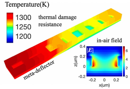
The electric field distribution only shows the anti-damage potential of the meta-deflector qualitatively. For quantitative analysis, some optothermal simulations are conducted to estimate the maximum laser intensity that the meta-reflector can handle. Figure 6a shows the temperature distribution in the unit element (its structure is presented as an inset image, which is composed of the 8 selected unit-cells in Table 1, area: 0.6 µm × 4.8 µm = 2.88 µm2) of the meta-deflector illustrated by a plane-wave laser with power 0.53 W. The unit-cells have similar temperature values from 1160 K to 1320 K. Under the illumination of different incident powers, the maximum temperature values in the 3D volume made of the unit element are reported in Figure 6b; 1683 K is the melting point of silicon. It is shown that the meta-deflector can handle the maximum laser power (0.68 W per 2.88 µm2), i.e., the laser density of 0.24 W/µm2.
4. Conclusions
In the study, meta-deflectors made of dielectric nanohole arrays are investigated to achieve anti-damage potential via tuning the distribution of the electric field. The rules of tuning the reflectance, phase, and electric field distribution through the geometrical parameters are investigated. The highest reflectance of nanoholes can be above 99% while the strongest electric fields can be tuned into the air zone. The in-air electric field does not interact with the silicon material directly, attenuating the optothermal effect that causes laser damage. One presentative meta-deflector is designed based on these nanoholes with in-air-hole field confinement. The 1st order of the meta-deflector has the highest reflectance of 55.74% and the steering angle is 8.8°. The reflectance sum of all the orders of the meta-deflector is 92.38%. The optothermal simulations show that the meta-deflector can theoretically handle a maximum laser density of 0.24 W/µm2. The study provides an approach to improve the anti-damage property of the reflective phase-control metasurfaces for the intense-light optical systems, which can be exploited in many applications, such as laser scalpel, laser cutting devices, etc.
Author Contributions
Conceptualization, F.T. and Y.W.; methodology, H.Y.; software, J.W.; investigation, H.Y.; resources, X.Y. and Z.Y.; writing—original draft preparation, H.Y.; writing—review and editing, H.Y. and F.T.; supervision, Y.W.; funding acquisition, H.Y., F.T., X.Y., and Z.Y. All authors have read and agreed to the published version of the manuscript.
Funding
This research was funded by National Natural Science Foundation of China, grant number [61705204, 61705206]; China Postdoctoral Science Foundation, grant number [2019M653486, 2019M651998]; Innovation and Development Foundation of China Academy of Engineering Physics, grant number [CX20200021]; Natural Science Foundation of Jiangsu Province, grant number [BK20190229]; Scientific Research Fund of Sichuan Provincial Science and Technology Department, grant number [2020YJ0137].
Conflicts of Interest
The authors declare no conflict of interest.
References
- Manes, K.; Spaeth, M.; Adams, J.; Bowers, M. Damage Mechanisms Avoided or Managed for NIF Large Optics. Fusion Sci. Technol. 2016, 69, 146–249. [Google Scholar] [CrossRef]
- Li, C.; Sun, Y.; Song, X.; Zhang, X.; Shi, Z.; Wang, F.; Ye, X.; Chen, S.; Sun, L.; Huang, J. Capping a glass thin layer on the etched surface via plasma chemical vapor deposition for improving the laser damage performance of fused silica. Opt. Express 2019, 27, 2268–2280. [Google Scholar] [CrossRef] [PubMed]
- Laixi, S.; Jin, H.; Hongjie, L.; Xin, Y.; Jingjun, W.; Xiaodong, J.; Liming, Y.; Wanguo, Z.; Weidong, W. Combination of reaction ion etching and dynamic chemical etching for improving laser damage resistance of fused silica optical surfaces. Opt. Lett. 2016, 41, 4464. [Google Scholar]
- Li, C.; Li, Q.; Sun, L.; Ye, X.; Chen, S.; Wu, Z.; Huang, J.; Wu, W.; Jiang, X. Effect of PVA coating on the electric field intensity distribution and laser damage performance of fused silica optics surfaces. Opt. Express 2018, 26, 19707–19717. [Google Scholar] [CrossRef] [PubMed]
- Ye, X.; Hu, X.; Tang, F.; Wu, J.; Yang, L.; Huang, J.; Zheng, W. Laser Field Manipulation and Laser Damage Resistance Property of Nanotextures on Fused Silica Optics. Results Phys. 2020, 18, 103262. [Google Scholar] [CrossRef]
- Jing, X.; Tian, Y.; Han, J.; Ma, J.; Jin, Y.; Shao, J.; Fan, Z. Polarization effect of femtosecond pulse breakdown in subwavelength antireflective relief grating. Opt. Commun. 2011, 284, 4220–4224. [Google Scholar] [CrossRef]
- Glybovski, S.B.; Tretyakov, S.A.; Belov, P.A.; Kivshar, Y.S.; Simovski, C.R. Metasurfaces: From microwaves to visible. Phys. Rep. 2016, 634, 1–72. [Google Scholar] [CrossRef]
- Genevet, P.; Capasso, F.; Aieta, F.; Khorasaninejad, M.; Devlin, R. Recent advances in planar optics: From plasmonic to dielectric metasurfaces. Optica 2017, 4, 139–152. [Google Scholar] [CrossRef]
- Hou-Tong, C.; Antoinette, J.T.; Nanfang, Y. A review of metasurfaces: Physics and applications. Rep. Prog. Phys. 2016, 79, 076401. [Google Scholar]
- Jahani, S.; Jacob, Z. All-dielectric metamaterials. Nat. Nanotechnol. 2016, 11, 23. [Google Scholar] [CrossRef]
- Hsiao, H.-H.; Chu, C.H.; Tsai, D.P. Fundamentals and Applications of Metasurfaces. Small Methods 2017, 1, 1600064. [Google Scholar] [CrossRef] [Green Version]
- Liu, L.; Zhang, X.; Kenney, M.; Su, X.; Xu, N.; Ouyang, C.; Shi, Y.; Han, J.; Zhang, W.; Zhang, S. Broadband Metasurfaces with Simultaneous Control of Phase and Amplitude. Adv. Mater. 2014, 26, 5031–5036. [Google Scholar] [CrossRef] [PubMed]
- Pors, A.; Bozhevolnyi, S.I. Gap plasmon-based phase-amplitude metasurfaces: Material constraints [Invited]. Opt. Mater. Express 2015, 5, 2448–2458. [Google Scholar] [CrossRef] [Green Version]
- Wu, J.; Tang, F.; Ma, J.; Li, Q.; Shang, S.; Chen, J.; Wu, Y.; Wang, Y.; Ye, X.; Zheng, W.; et al. Angle-sensitive dynamic optical modulation based on Huygens metasurfaces. Results Phys. 2020, 18, 103226. [Google Scholar] [CrossRef]
- Kwon, D.H.; Ptitcyn, G.; Díaz-Rubio, A.; Tretyakov, S.A. Transmission Magnitude and Phase Control for Polarization-Preserving Reflectionless Metasurfaces. Phys. Rev. Appl. 2018, 9, 034005. [Google Scholar] [CrossRef] [Green Version]
- Lingling, H.; Shuang, Z.; Thomas, Z. Metasurface holography: From fundamentals to applications. Nanophotonics 2018, 7, 1169–1190. [Google Scholar] [CrossRef]
- Shalaev, M.I.; Sun, J.; Tsukernik, A.; Pandey, A.; Nikolskiy, K.; Litchinitser, N.M. High-Efficiency All-Dielectric Metasurfaces for Ultracompact Beam Manipulation in Transmission Mode. Nano Lett. 2015, 15, 6261–6266. [Google Scholar] [CrossRef] [PubMed] [Green Version]
- Decker, M.; Staude, I.; Falkner, M.; Dominguez, J.; Neshev, D.N.; Brener, I.; Pertsch, T.; Kivshar, Y.S. High-Efficiency Dielectric Huygens’ Surfaces. Adv. Opt. Mater. 2015, 3, 813–820. [Google Scholar] [CrossRef] [Green Version]
- Pors, A.; Nielsen, M.G.; Bernardin, T.; Weeber, J.-C.; Bozhevolnyi, S.I. Efficient unidirectional polarization-controlled excitation of surface plasmon polaritons. Light Sci. Appl. 2014, 3, e197. [Google Scholar] [CrossRef] [Green Version]
- Khorasaninejad, M.; Chen, W.T.; Zhu, A.Y.; Oh, J.; Devlin, R.C.; Rousso, D.; Capasso, F. Multispectral Chiral Imaging with a Metalens. Nano Lett. 2016, 16, 4595–4600. [Google Scholar] [CrossRef]
- Segal, N.; Keren-Zur, S.; Hendler, N.; Ellenbogen, T. Controlling light with metamaterial-based nonlinear photonic crystals. Nat. Photonics 2015, 9, 180. [Google Scholar] [CrossRef]
- Husu, H.; Siikanen, R.; Mäkitalo, J.; Lehtolahti, J.; Laukkanen, J.; Kuittinen, M.; Kauranen, M. Metamaterials with Tailored Nonlinear Optical Response. Nano Lett. 2012, 12, 673–677. [Google Scholar] [CrossRef]
- Chu, P.; Chen, J.; Xiong, Z.; Yi, Z. Controllable frequency conversion in the coupled time-modulated cavities with phase delay. Opt. Commun. 2020, 476, 126338. [Google Scholar] [CrossRef]
- Monti, A.; Alù, A.; Toscano, A.; Bilotti, F. Surface Impedance Modeling of All-Dielectric Metasurfaces. IEEE Trans. Antennas Propag. 2020, 68, 1799–1811. [Google Scholar] [CrossRef]
- Moitra, P.; Slovick, B.A.; Li, W.; Kravchencko, I.I.; Briggs, D.P.; Krishnamurthy, S.; Valentine, J. Large-Scale All-Dielectric Metamaterial Perfect Reflectors. ACS Photonics 2015, 2, 692–698. [Google Scholar] [CrossRef]
- Lin, R.J.; Su, V.-C.; Wang, S.; Chen, M.K.; Chung, T.L.; Chen, Y.H.; Kuo, H.Y.; Chen, J.-W.; Chen, J.; Huang, Y.-T.; et al. Achromatic metalens array for full-colour light-field imaging. Nat. Nanotechnol. 2019, 14, 227–231. [Google Scholar] [CrossRef] [PubMed]
- Zhang, C.; Divitt, S.; Fan, Q.; Zhu, W.; Agrawal, A.; Xu, T.; Lezec, H.J. All-dielectric Deep Ultraviolet Metasurfaces. In CLEO: QELS_Fundamental Science; Optical Society of America: Washington, DC, USA, 2019; p. FM3C–3. [Google Scholar]
- Tang, F.; Ye, X.; Li, Q.; Wang, Y.; Yu, H.; Wu, W.; Li, B.; Zheng, W. Dielectric Metalenses at Long-wave Infrared Wavelengths: Multiplexing and Spectroscope. Results Phys. 2020, 18, 103215. [Google Scholar] [CrossRef]
- Khorasaninejad, M.; Capasso, F. Broadband Multifunctional Efficient Meta-Gratings Based on Dielectric Waveguide Phase Shifters. Nano Lett. 2015, 15, 6709–6715. [Google Scholar] [CrossRef] [PubMed]
- Wu, Y.; Tang, F.; Chen, J.; Shang, S.; Wu, J.; Chen, S.; Chen, Y.; Ye, X.; Yang, L. Design of high-efficiency all-dielectric polymer meta-surfaces beam deflection blazed grating. Results Phys. 2020, 17, 103094. [Google Scholar] [CrossRef]
- Yu, Y.F.; Zhu, A.Y.; Paniagua-Domínguez, R.; Fu, Y.H.; Luk’yanchuk, B.; Kuznetsov, A.I. High-transmission dielectric metasurface with 2π phase control at visible wavelengths. Laser Photon. Rev. 2015, 9, 412–418. [Google Scholar] [CrossRef]
- Yi, Z.; Li, J.; Lin, J.; Qin, F.; Chen, X.; Yao, W.-T.; Liu, Z.; Cheng, S.; Wu, P.; Li, H. Broadband polarization-insensitive and wide-angle solar energy absorber based on tungsten ring-disc array. Nanoscale 2020, 12, 23077–23083. [Google Scholar] [CrossRef] [PubMed]
- Zhang, Y.; Wu, P.; Zhou, Z.; Chen, X.; Yi, Z.; Zhu, J.; Zhang, T.; Jile, H. Study on temperature adjustable terahertz metamaterial absorber based on vanadium dioxide. IEEE Access 2020, 8, 85154–85161. [Google Scholar] [CrossRef]
- Zhao, F.; Chen, X.; Yi, Z.; Qin, F.; Tang, Y.; Yao, W.; Zhou, Z.; Yi, Y. Study on the solar energy absorption of hybrid solar cells with trapezoid-pyramidal structure based PEDOT: PSS/c-Ge. Sol. Energy 2020, 204, 635–643. [Google Scholar] [CrossRef]
- Yu, P.; Yang, H.; Chen, X.; Yi, Z.; Yao, W.; Chen, J.; Yi, Y.; Wu, P. Ultra-wideband solar absorber based on refractory titanium metal. Renew. Energy 2020, 158, 227–235. [Google Scholar] [CrossRef]
- Chen, T.; Chang, F.; Huang, B.; Yu, P. Optical absorption enhancement in silicon nanohole arrays for photovoltaics. In Proceedings of the 2011 37th IEEE Photovoltaic Specialists Conference, Seattle, WA, USA, 19–24 June 2011; pp. 002855–002857. [Google Scholar]
- Xia, Z.; Qin, X.; Wu, Y.; Pan, Y.; Zhou, J.; Zhang, Z. Efficient broadband light absorption in elliptical nanohole arrays for photovoltaic application. Opt. Lett. 2015, 40, 5814–5817. [Google Scholar] [CrossRef]
- Sun, S.; Zhou, Z.; Zhang, C.; Gao, Y.; Duan, Z.; Xiao, S.; Song, Q. All-Dielectric Full-Color Printing with TiO2 Metasurfaces. ACS Nano 2017, 11, 4445–4452. [Google Scholar] [CrossRef] [PubMed]
- Zhao, W.; Jiang, H.; Liu, B.; Song, J.; Jiang, Y.; Tang, C.; Li, J. Dielectric Huygens’ Metasurface for High-Efficiency Hologram Operating in Transmission Mode. Sci. Rep. 2016, 6, 30613. [Google Scholar] [CrossRef] [PubMed] [Green Version]
- Geffrin, J.M.; García-Cámara, B.; Gómez-Medina, R.; Albella, P.; Froufe-Pérez, L.S.; Eyraud, C.; Litman, A.; Vaillon, R.; González, F.; Nieto-Vesperinas, M.; et al. Magnetic and electric coherence in forward- and back-scattered electromagnetic waves by a single dielectric subwavelength sphere. Nat. Commun. 2012, 3, 1171. [Google Scholar] [CrossRef] [PubMed]
Figure 1.
Schematic of the studied unit-cell in which a Si rectangular nanohole (length L, width W, height H) is located on a SiO2 substrate. The lattice period is constant P = 600 nm. The x-polarized incidence is injected from the bottom.
Figure 1.
Schematic of the studied unit-cell in which a Si rectangular nanohole (length L, width W, height H) is located on a SiO2 substrate. The lattice period is constant P = 600 nm. The x-polarized incidence is injected from the bottom.

Figure 2.
Optical properties of the unit-cells of Si nanoholes: (a) reflectance and (b) phase of light reflected by the unit-cells as a function of L and W. Here, the height H is 200 nm, and the lattice period P is 600 nm.
Figure 2.
Optical properties of the unit-cells of Si nanoholes: (a) reflectance and (b) phase of light reflected by the unit-cells as a function of L and W. Here, the height H is 200 nm, and the lattice period P is 600 nm.

Figure 3.
Electric field distributions of the 8 selected unit-cells: (a–h) normalized electric field distribution on the x-y plane with z = 100 nm; (i–p) normalized electric field distribution on the x-z plane with y = 0.
Figure 3.
Electric field distributions of the 8 selected unit-cells: (a–h) normalized electric field distribution on the x-y plane with z = 100 nm; (i–p) normalized electric field distribution on the x-z plane with y = 0.

Figure 4.
Electromagnetic polarizabilities of the 8 selected unit-cells: (a) effective electric polarizability ; (b) effective magnetic polarizability . The solid curves are the electromagnetic polarizabilities of an ideal reflective Huygens source with phase covering the 0-2π range.
Figure 4.
Electromagnetic polarizabilities of the 8 selected unit-cells: (a) effective electric polarizability ; (b) effective magnetic polarizability . The solid curves are the electromagnetic polarizabilities of an ideal reflective Huygens source with phase covering the 0-2π range.

Figure 5.
Beam-steering performance of the reflective meta-deflector: (a) local electric field distributions on the x-y plane with z = 100 nm and on the x-z plane with y = 0. The red rectangular frames indicate the nanoholes in the silicon film; (b) reflectance of the different diffraction orders of the meta-reflector.

Figure 6.
Photothermal analysis of the meta-deflector: (a) the temperature distribution in the unit element (area: 2.88 µm2) of the deflector illustrated by a plane-wave laser with power 0.53 W. The inset image shows the unit-element structure; (b) the maximum value of temperature in the 3D volume of (a) under the illumination of different incident power.


Table 1.
Unit-cells selected for designing meta-deflectors. The 0-2π phase range is discretized into eight segments with an interval of π/4.
Table 1.
Unit-cells selected for designing meta-deflectors. The 0-2π phase range is discretized into eight segments with an interval of π/4.
| Phase Point | 0 | π/4 | π/2 | 3π/4 | π | 5π/4 | 3π/2 | 7π/4 |
|---|---|---|---|---|---|---|---|---|
| Phase offset | 0.012 | 0.059 | 0.052 | 0.055 | 0.07 | 0.207 | 0.183 | 0.072 |
| Reflectance | 0.995 | 0.949 | 0.945 | 0.733 | 0.38 | 0.796 | 0.992 | 0.994 |
| W(nm) | 425 | 500 | 355 | 270 | 485 | 460 | 430 | 425 |
| L(nm) | 365 | 260 | 555 | 555 | 550 | 520 | 525 | 425 |
Publisher’s Note: MDPI stays neutral with regard to jurisdictional claims in published maps and institutional affiliations. |
© 2021 by the authors. Licensee MDPI, Basel, Switzerland. This article is an open access article distributed under the terms and conditions of the Creative Commons Attribution (CC BY) license (https://creativecommons.org/licenses/by/4.0/).
Share and Cite
MDPI and ACS Style
Yu, H.; Tang, F.; Wu, J.; Yi, Z.; Ye, X.; Wang, Y. Meta-Deflectors Made of Dielectric Nanohole Arrays with Anti-Damage Potential. Photonics 2021, 8, 107. https://doi.org/10.3390/photonics8040107
AMA Style
Yu H, Tang F, Wu J, Yi Z, Ye X, Wang Y. Meta-Deflectors Made of Dielectric Nanohole Arrays with Anti-Damage Potential. Photonics. 2021; 8(4):107. https://doi.org/10.3390/photonics8040107
Chicago/Turabian StyleYu, Haichao, Feng Tang, Jingjun Wu, Zao Yi, Xin Ye, and Yiqun Wang. 2021. "Meta-Deflectors Made of Dielectric Nanohole Arrays with Anti-Damage Potential" Photonics 8, no. 4: 107. https://doi.org/10.3390/photonics8040107
Note that from the first issue of 2016, this journal uses article numbers instead of page numbers. See further details here.