A Monolithically Integrated Laser-Photodetector Chip for On-Chip Photonic and Microwave Signal Generation


1
Key Laboratory of Semiconductor Materials Science, Institute of Semiconductors, Chinese Academy of Sciences, Beijing 100083, China
2
Center of Materials Science and Optoelectronics Engineering, University of Chinese Academy of Sciences, Beijing 100049, China
3
Beijing Key Laboratory of Low Dimensional Semiconductor Materials and Devices, Beijing 100083, China
*
Author to whom correspondence should be addressed.
Photonics 2019, 6(4), 102; https://doi.org/10.3390/photonics6040102
Submission received: 29 August 2019
/
Revised: 20 September 2019
/
Accepted: 29 September 2019
/
Published: 30 September 2019
(This article belongs to the Special Issue Semiconductor Laser Dynamics: Fundamentals and Applications)
Abstract
:An Indium-phosphide-based monolithically integrated photonic chip comprising of an amplified feedback laser (AFL) and a photodetector was designed and fabricated for on-chip photonic and microwave generation. Various waveforms including single tone, multi-tone, and chaotic signal generation were demonstrated by simply adjusting the injection currents applied to the controlling electrodes. The evolution dynamics of the photonic chip was characterized. Photonic microwave with frequency separation tunable from 26.3 GHz to 34 GHz, chaotic signal with standard bandwidth of 12 GHz were obtained. An optoelectronic oscillator (OEO) based on the integrated photonic chip was demonstrated without using any external electrical filter and photodetector. Tunable microwave outputs ranging from 25.5 to 26.4 GHz with single sideband (SSB) phase noise less than −90 dBc/Hz at a 10-kHz offset from the carrier frequency were realized.
1. Introduction
Photonic microwave technologies have important applications in the field of radio over fiber system, radar, lidar, unmanned driving, etc. The development of photonic microwave technologies has received much attention. The generation of photonic microwave signals is generally based on discrete devices, including multiple active and passive devices, which are bulky, costly and lossy. With the development of photonic integration technology, photonic integrated chips are showing their potential in photonic microwave generation and processing [1,2], with the possibility to greatly reduce the system complexity, footprint, performance, and the cost.
To generate photonic microwave, at least two laser modes or sidebands are required, so that the heterodyning signal after photodetection will produce a microwave signal corresponding to the mode separation between the modes. Among various types of photonic integrated microwave generators, dual-mode semiconductor lasers are typical ones. Many dual-mode structures have been proposed, including the integration of two semiconductor lasers in series [3,4] or parallel [5], integrated feedback cavity lasers [6,7], etc. By controlling the mode separation between the two modes, photonic microwave with frequency ranging from GHz to THz can be obtained [3,7]. However, due to the lack of the necessary phase correlation between the laser modes, the heterodyning signal usually has a linewidth on the order of several or tens of MHz, which limits their potential applications in many fields. To address the problem, many techniques such as optical injection locking [8,9], electrical modulation [10], or optoelectronic oscillation [11] have been proposed, which have greatly improved the signal quality of the integrated photonic microwave source to a level comparable or even superior to that obtained from electrical devices.
Another type of photonic microwave is the chaotic signal, which can be generated by using semiconductor lasers under optical injection [12,13], optical feedback [14,15] or optoelectric feedback [16,17]. Photonic integration technology provides a solution to combine the laser cavity and the feedback cavity or injection sources into a single chip [7,18,19,20] so that the needs for free-space or fiber-based feedback/injection are eliminated. Chaotic signals with bandwidth over tens of GHz have been demonstrated [21,22].
In the above-mentioned structure, however, external photodetectors were required to generate the microwave signal. In order to further include more functionality, the photodetectors have been integrated on-chip [23,24]. In [23,24], the photodetectors were integrated with two distributed feedback (DFB) lasers which were combined by a multimode interference (MMI) coupler. The tuning range of the on-chip-generated microwave signal could reach several tens of GHz. However, the active and passive integration requires additional regrowth process. Besides, the use of the MMI coupler resulted in a long device length of several mm.
In this paper, we present a simple Indium-phosphide(InP)-based monolithically integrated photonic microwave generator comprising of an amplified feedback laser (AFL) and a photodetector for on-chip photonic and microwave generation. The integrated photonic chip shares the same active material, no additional regrowth is required. The total length of the chip was only about 1.17 mm. By adjusting the injection currents applied on the controlling electrodes, microwaves with various waveforms including single tone, multitone and chaotic signal could be realized. Tunable microwave ranging from 26.3 GHz to 34 GHz, chaotic signal with standard bandwidth of 12 GHz were obtained. Furthermore, an optoelectronic oscillator (OEO) was constructed using the integrated photonic chip. Thanks to the multifunctionality of the integrated chip, there was no need for external lasers source, external microwave filter or external photodetector in the OEO system. Tunable microwave outputs ranging from 25.5 GHz to 26.4 GHz, with single sideband (SSB) phase noise of less than −90 dBc/Hz at 10 kHz offset from the carrier frequency were demonstrated.
2. Device Structure and Fabrication Process
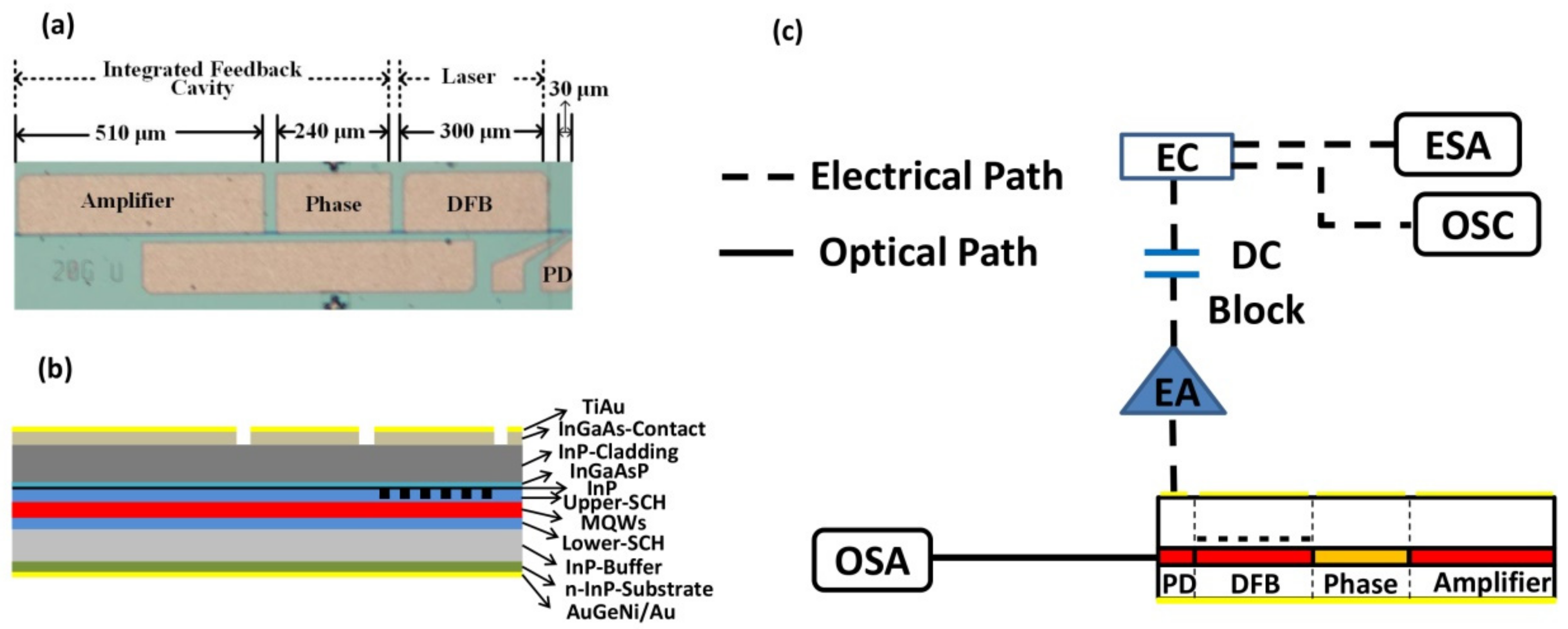
The integrated laser-photodetector-chip comprises an amplifier feedback laser and a photodetector, as shown in Figure 1a. The AFL consists of a DFB section, a phase section, and an amplifier section. The DFB section functions as a laser source, while the phase section and the amplifier section forms an integrated feedback cavity, allowing the adjustment of the feedback phase and the feedback strength through current injection. The AFL can work in single-mode (S), period one (P1) state, period two (P2), chaos (C) state and dual-mode (D) state by controlling the bias currents. Normally, simple control of the amplifier’s bias current will suffice to go through all of the states [7]. The on-chip integrated photodetector directly converts the various dynamic states from the optical domain into the electrical domain. The lengths of the DFB section, the phase section, the amplifier section, and the photodetector section are 300 μm, 240 μm, 510 μm, and 30 μm, respectively. Each adjacent section was electronically isolated by a 20-μm-long isolation region to prevent the electric crosstalk between adjacent sections. The AFL section and the photodetector section shared the same multiple quantum wells (MQWs) structure, which was grown on an S-doped n-type InP substrate by using metal-organic chemical vapor deposition (MOCVD). The schematic illustration of the monolithically integrated laser-photodetector chip is shown in Figure 1b. The epitaxial structure consists of six pairs of compressively strained InGaAsP MQWs sandwiched between two 120-nm-thick InGaAsP separated confinement heterostructure (SCH) layers. A gain-coupled Bragg grating was defined holographically on the upper-SCH layer of the DFB section. Then a p-InP cladding and a p-InGaAs contact layer were regrown by MOCVD. A 3-μm-wide ridge waveguide was fabricated by wet etching. The electrical isolation region between two adjacent sections was formed by etching the p-InGaAs contact layer off, followed by He+ ion implanting, which provided a ~6 kΩ electrical resistance. A Ti-Au metal layer was sputtered on the p-type InGaAs contact layer to form a p-contact. Then the substrate is thinned, and Au-Ge-Ni/Au was evaporated on the backside. Finally, n-contact was formed after rapid thermal annealing.
3. Experimental Setup and Results
3.1. Dynamic States
The integrated laser-photodetector chip was mounted on a ground-signal-ground (GSG) subcarrier with the S-electrode connected to the p-contact of the photodetector to extract the on-chip electrical signal, as shown in Figure 1c. An electrical amplifier (EA) with 27-dB gain was used to boost the electrical signal. After passing through a DC block, the amplified electrical signal was split into two parts by a 50:50 electrical coupler to monitor the temporal waveforms and the RF spectra by using a real-time oscilloscope (OSC) (Tektronix DPO70000SX, 70-GHz bandwidth, Tektronix, Inc. Beaverton, OR, USA) and an electrical spectrum analyzer (ESA) (Agilent PXA N9030 A, 50-GHz bandwidth, Agilent Technologies Inc. Santa Clara, CA, USA), respectively. The optical spectra were measured by coupling the emission light from the photodetector-side using an optical signal analyzer (OSA) (Advantest Q8384, 0.01-nm resolution, Advantest Corporation, Tokyo, Japan). During the measurement, the working temperature was maintained at 20 °C by a thermo-electric cooler (TEC). Under −2.5 V bias condition, the on-chip photodetector had a −3 dB bandwidth of approximately 13 GHz (−10 dB bandwidth of ~26.5 GHz), which was measured by a 50-GHz vector network analyzer (VNA) (HP 8510c, Hewlett-Packard, Palo Alto, CA, USA ).
When characterizing the dynamic states of the chip, the injection currents of the DFB section and phase section were fixed at (IDFB, IPhase) = (78, 3) mA, and the dynamic state was controlled by tuning the amplifier section’s injection currents. Figure 2 shows the optical spectra, radio frequency (RF) spectra, temporal waveforms and phase portrait of the device outputs under different amplifier currents. When IA = 0 mA, the chip works at the single-mode (S) state (Figure 2a) with side-mode suppression ratio (SMSR) > 55 dB. The corresponding temporal waveform shows a constant level. Accordingly, the phase portrait is a small spot. The RF spectrum reveals the characteristic relaxation-oscillation frequency of the DFB laser is around ~9 GHz, as shown in Figure 2(a-ii). When IA increases to 9 mA, as shown in Figure 2(b-i), the chip enters into the period-one (P1) state, and the temporal waveform shows a single period oscillation trace. The P1 state is also confirmed from the RF spectrum and the phase portrait as well, where a fundamental frequency appears around 5.5 GHz and the trajectories of phase portrait show clear limit cycle feature. Further increasing IA to 18.5 mA, the chip is driven into the chaos (C) state, which can be confirmed from Figure 2c. The optical spectrum has been considerably broadened and the corresponding power spectrum covers a broad frequency range. Besides, the temporal waveform fluctuates dramatically, and the phase portrait shows a widely scattered distribution in a large area. As shown in Figure 2(c-ii), the chaotic electrical signal obtained from the on-chip photodetector has a standard bandwidth up to 12 GHz, where the standard bandwidth is defined as the span between the DC and the frequency where 80% of the energy is contained with the power spectrum. Further increasing IA from 18.5 mA to 24.5 mA, the output gradually evolves out of the C state and into a dual-mode (D) state. A typical optical spectrum of the dual-mode emission is presented in Figure 2(d-i). The RF spectrum in Figure 2(d-ii) shows an oscillation peak at ~26.3 GHz, corresponding to the dual-mode spacing. Due to the amplitude imbalance and the lack of coherence of the two laser modes, the temporal waveform does not show a well-defined sinusoidal shape, and the corresponding phase portrait also shows a limit cycle feature, but the traces are broadened compared to the P1 state.
In our previous work [7,25,26], we have theoretically and experimentally demonstrated that in the dual-mode state, the beating frequency of the AFL’s emission increases with the increase of the feedback strength as IA increases. The relationship between the frequency of the on-chip generated microwave signal and IA of the integrated laser-photodetector chip was investigated by increasing IA from 24.5 mA to 50.5 mA with a 2-mA step. When IA was fixed at 42.5 mA, the RF spectra were shown in Figure 3a, and the 3 dB linewidth of the beating RF signal was 7.6 MHz. As shown in Figure 3b, the on-chip generated microwave signal can be tuned from 26.3 GHz to 34 GHz.
3.2. High-Quality Microwave Signal Generation
The dual-mode AFL can function as an active microwave photonic filter (MPF) and a pump source to start the optoelectronic oscillation in an optoelectronic oscillator (OEO) [11,27]. However, a discrete photodetector is still needed to achieve O/E conversion. By using the integrated laser-photodetector chip, a frequency tunable OEO with on-chip microwave generation capability was constructed.
The system diagram of the proposed OEO is shown in Figure 4, which contains an optical feedback loop (O-Loop) and an optoelectronic oscillation loop (OE-Loop). When working, the dual-mode signal travels through a circulator (Cir), a 99:1 optical coupler (OC), a 0.3-km-long single-mode fiber, a Mach-Zehnder modulator (MZM) driven by the amplified beating signal, which was extracted from the on-chip integrated photodetector and amplified by two electrical amplifiers (EA) with a total gain of ~60 dB (OE-Loop). Then, the modulated dual-mode light was sent to a 1-km-long single-mode fiber and injected back to chip through port 1 of the Cir to accomplish the O-Loop and OE-Loop. The dual-loop configuration performs a fine mode selection, which helps to suppress the unwanted cavity modes and improve the side-mode suppression ratio (SMSR) of the oscillation modes. With the assistance of O-Loop, two kinds of injection locking will happen inside the integrated laser-photodetector chip simultaneously. One is the delayed self-injection locking of an individual mode by its fiber-delayed replica. The delayed self-injection will considerably reduce the laser linewidth [9,28]. Besides, the equivalent bandwidth of the MPF will also be narrowed due to the narrowed beating signals. The other one is the mutual-injection locking between laser modes and the modulation sidebands. As a result, two laser modes will be synchronized at a fixed mode spacing and phase difference. Accordingly, high-quality beating signal originated from the dual-mode will be generated. The oscillation frequency was determined by the dual-mode spacing, which can be tuned with the injection current of IA. In the O-Loop, the polarization controllers (PCs) were used to match the polarization state between the feedback signal to the MZM and the integrated laser-photodetector, and the variable optical attenuator (VOA) was used control the feedback strength, respectively. The output signal was monitored through an OSA and an ESA.
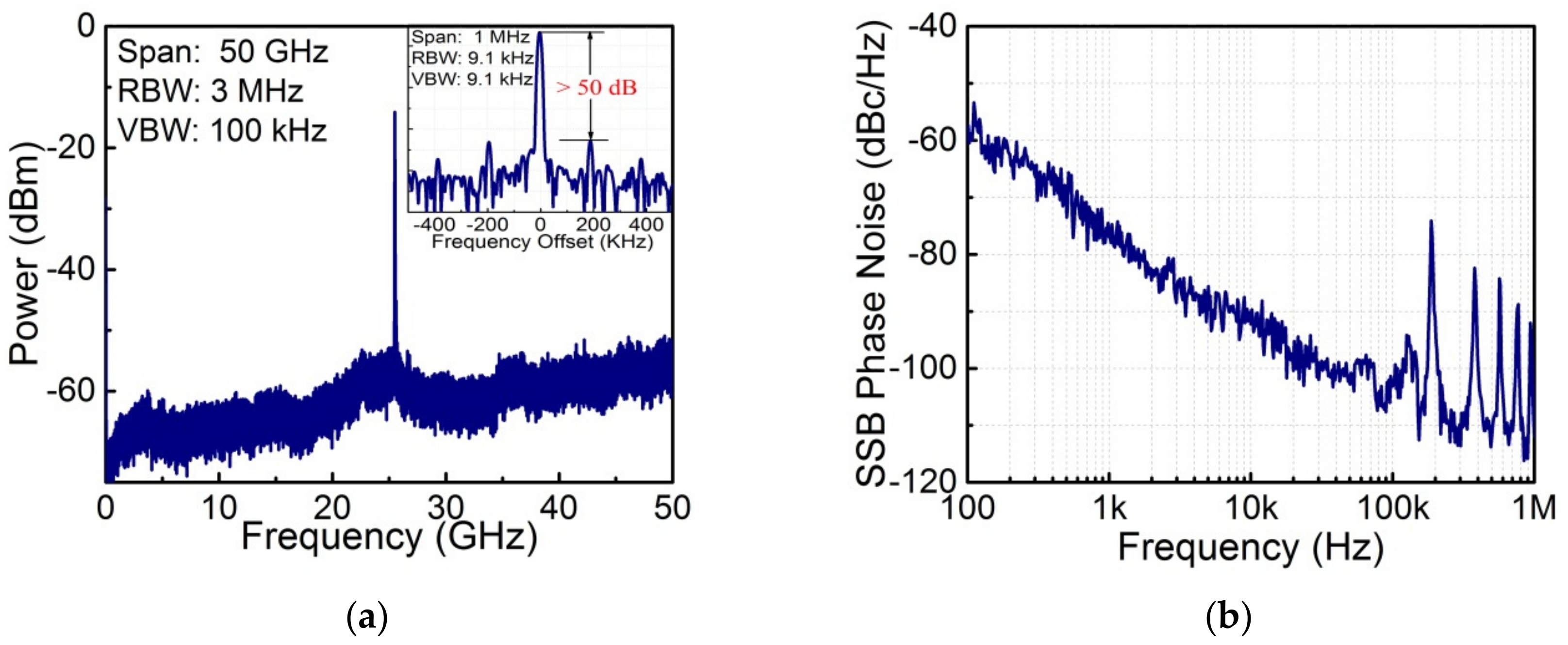
When IDFB, IPhase, and IA were biased at 75 mA, 1.5 mA, 42 mA, respectively, the integrated laser-photodetector chip exhibited a dual-mode emission with a mode spacing of 26.05 GHz. The dual-mode optical signal was converted to the electrical domain by the on-chip photodetector and served as the oscillation seeding to start the optoelectronic oscillation. At an optical feedback power of −12 dBm (measured at port 1 of the Cir), the OEO started to oscillate at the beating frequency. Figure 5a shows the generated microwave signal. The inset shows the zoom-in view of this signal in a 1-MHz span. The SSB phase noise spectrum of the obtained microwave signal was measured by the build-in phase noise module of the ESA. As shown in Figure 5b, the SSB phase noise of the 26.05 GHz signal is −92.2 dBc/Hz at a 10-kHz frequency offset of the carrier frequency. Other spurious modes have a maximal phase noise of <−73 dBc/Hz, indicating a good spectral purity of the OEO.
By tuning the injection current of IA from 40 mA to 46 mA, the output frequency of the OEO can be continuously tunable from 25.5 GHz to 26.4 GHz, as shown in Figure 6a. The SSB phase noise of the generated microwave signals was all below −90 dBc/Hz at a 10-kHz frequency offset over the whole frequency tuning range, as shown in Figure 6b. Due to the limited bandwidth of the photodetector, a further increase of the frequency tuning range was not attained. A widely frequency-tunable OEO can be expected if the bandwidth of the integrated photodetector can be further optimized.
4. Discussion
Compared with [24], the integrated photonic chip is smaller, which only includes an AFL and a photodetector. The dual-mode light is generated by the AFL, which oscillates in the same resonant cavity. So, the phase correlation between the two modes is usually better than [24] in terms of optical linewidth and heterodyning microwave signal. With this integrated chip, both optical and electronic chaotic signal can be directly generated. The proposed frequency tunable OEO based on the integrated laser-photodetector chip shows a further step toward highly integrated on-chip OEO system. The small frequency adjustment range of the system can be improved by optimizing the material structure of the detector, adopting PIN photodiodes (PIN-PD) or uni-traveling-carrier photodiodes (UTC-PD) type detector structure using the butt-joint growth technique to increase the bandwidth of the detector.
5. Conclusions
In conclusion, we demonstrated an InP-based monolithically integrated photonic chip including an AFL and a detector for on-chip photonic and microwave generation. The device shows rich dynamic states, including single tone, multi-tone, and chaotic signal. The output optical signal can be directly converted into electrical signals by the on-chip photodetector. Single-tone photonic microwave signal with a frequency tunable from 26.3 GHz to 34 GHz and chaotic signal with a standard bandwidth of 12 GHz was obtained. An OEO based on the integrated photonic chip was built. High-quality microwave signal tunable 25.5 GHz to 26.4 GHz were obtained without the using of external electrical filters and photodetectors. SSB phase noise less than −90 dBc/Hz at a 10-kHz offset from the carrier frequency over the entire frequency range was realized.
Author Contributions
Conceptualization, L.Z., D.L., G.C.; methodology, G.C., H.Q.; formal analysis, G.C., H.Q.; investigation, H.Q.; writing—original draft preparation, H.Q.; writing—review and editing, D.L.; visualization, H.Q., G.C.; supervision, D.L., L.Z.; project administration, D.L.; funding acquisition, L.Z., D.L.
Funding
This research was funded by National Key Research & Development (R&D) Plan, grant number 2016YFB0402301 and the National Natural Science Foundation of China, grant number: 61975197.
Conflicts of Interest
The authors declare no conflict of interest.
References
- Marpaung, D.; Roeloffzen, C.; Heideman, R.; Leinse, A.; Sales, S.; Capmany, J. Integrated microwave photonics. Laser Photonics Rev. 2013, 7, 506–538. [Google Scholar] [CrossRef] [Green Version]
- Capmany, J.; Muñoz, P. Integrated Microwave Photonics for Radio Access Networks. J. Lightwave Technol. 2014, 32, 2849–2861. [Google Scholar] [CrossRef]
- Kim, N.; Shin, J.; Sim, E.; Lee, C.W.; Yee, D.-S.; Min, Y.J.; Jang, Y.; Park, K.H. Monolithic dual-mode distributed feedback semiconductor laser for tunable continuous-wave terahertz generation. Opt. Express 2009, 17, 13851–13859. [Google Scholar] [CrossRef] [PubMed]
- Zhang, C.; Liang, S.; Zhu, H.; Wang, W. Widely tunable dual-mode distributed feedback laser fabricated by selective area growth technology integrated with Ti heaters. Opt. Lett. 2013, 38, 3050–3053. [Google Scholar] [CrossRef] [PubMed]
- Kong, D.; Zhu, H.; Liang, S.; Yu, W.; Lou, C.; Zhao, L. All-optical clock recovery using parallel ridge-width varied DFB lasers integrated with Y-branch waveguide coupler. Opt. Commun. 2012, 285, 311–314. [Google Scholar]
- Bauer, S.; Brox, O.; Kreissl, J.; Sahin, G.; Sartorius, B. Optical microwave source. Electron. Lett. 2002, 38, 334–335. [Google Scholar] [CrossRef]
- Yu, L.; Lu, D.; Pan, B.; Zhao, L.; Wu, J.; Xia, G.; Wu, Z.; Wang, W. Monolithically integrated amplified feedback lasers for high-quality microwave and broadband chaos generation. J. Lightwave Technol. 2014, 32, 3595–3601. [Google Scholar] [CrossRef]
- Yu, L.; Lu, D.; Zhao, L.; Li, Y.; Ji, C.; Pan, J.; Zhu, H.; Wei, W. Wavelength and Mode-Spacing Tunable Dual-Mode Distributed Bragg Reflector Laser. IEEE Photonics. Technol. Lett. 2013, 25, 576–579. [Google Scholar] [CrossRef]
- Pan, B.; Lu, D.; Sun, Y.; Yu, L.; Zhang, L.; Zhao, L. Tunable optical microwave generation using self-injection locked monolithic dual-wavelength amplified feedback laser. Opt. Lett. 2014, 39, 6395–6398. [Google Scholar] [CrossRef]
- Yu, L.; Lu, D.; Sun, Y.; Zhao, L. Tunable photonic microwave generation by directly modulating a dual-wavelength amplified feedback laser. Opt. Commun. 2015, 345, 57–61. [Google Scholar] [CrossRef]
- Lu, D.; Pan, B.; Chen, H.; Zhao, L. Frequency-tunable optoelectronic oscillator using a dual-mode amplified feedback laser as an electrically controlled active microwave photonic filter. Opt. Lett. 2015, 40, 4340–4343. [Google Scholar] [CrossRef] [PubMed]
- Simpson, T.B.; Liu, J.M.; Gavrielides, A.; Kovanis, V.; Alsing, P.M. Period-doubling route to chaos in a semiconductor laser subject to optical injection. Appl. Phys. Lett. 1994, 64, 3539–3541. [Google Scholar] [CrossRef]
- Wang, A.-B.; Wang, Y.-C.; Wang, J.-F. Route to broadband chaos in a chaotic laser diode subject to optical injection. Opt. Lett. 2009, 34, 1144–1146. [Google Scholar] [CrossRef] [PubMed] [Green Version]
- Mork, J.; Mark, J.; Tromborg, B. Route to chaos and competition between relaxation oscillations for a semiconductor laser with optical feedback. Phys. Rev. Lett. 1990, 65, 1999–2002. [Google Scholar] [CrossRef] [PubMed]
- Mukai, T.; Otsuka, K. New route to optical chaos: Successive-subharmonic-oscil- lation cascade in a semiconductor laser coupled to an external cavity. Phys. Rev. Lett. 1985, 55, 1711–1714. [Google Scholar] [CrossRef]
- Lin, F.Y.; Liu, J.M. Nonlinear dynamics of a semiconductor laser with delayed negative optoelectronic feedback. IEEE J. Quantum Electron. 2003, 39, 562–568. [Google Scholar] [CrossRef]
- Tang, S.; Liu, J.M. Chaotic pulsing and quasi-periodic route to chaos in a semiconductor laser with delayed opto-electronic feedback. IEEE J. Quantum Electron. 2001, 37, 329–336. [Google Scholar] [CrossRef]
- Sunada, S.; Harayama, T.; Arai, K.; Yoshimura, K.; Davis, P.; Tsuzuki, K.; Uchida, A. Chaos laser chips with delayed optical feedback using a passive ring waveguide. Opt. Express 2011, 19, 5713–5724. [Google Scholar] [CrossRef]
- Bauer, S.; Brox, O.; Kreissl, J.; Sartorius, B.; Radziunas, M.; Sieber, J.; Wünsche, H.-J.; Henneberger, F. Nonlinear dynamics of semiconductor lasers with active optical feedback. Phys. Rev. E 2004, 69, 016206. [Google Scholar] [CrossRef] [Green Version]
- Wünsche, H.-J.; Bauer, S.; Kreissl, J.; Ushakov, O.; Korneyev, N.; Henneberger, F.; Wille, E. Synchronization of delay-coupled oscillators: A study of semiconductor lasers. Phys. Rev. Lett. 2005, 94, 163901. [Google Scholar] [CrossRef]
- Pan, B.; Lu, D.; Zhao, L. Broadband Chaos Generation Using Monolithic Dual-Mode Laser With Optical Feedback. IEEE Photonics. Technol. Lett. 2015, 27, 2516–2519. [Google Scholar] [CrossRef]
- Wu, J.-G.; Zhao, L.-J.; Wu, Z.-M.; Lu, D.; Tang, X.; Zhong, Z.-Q.; Xia, G.-Q. Direct generation of broadband chaos by a monolithic integrated semiconductor laser chip. Opt. Express 2013, 21, 23358–23364. [Google Scholar] [CrossRef] [PubMed]
- Dijk, F.V.; Kervella, G.; Lamponi, M.; Chtioui, M.; Carpintero, G. Integrated InP Heterodyne Millimeter Wave Transmitter. IEEE Photonics. Technol. Lett. 2014, 26, 965–968. [Google Scholar] [CrossRef]
- Lo, M.C.; Zarzuelo, A.; Guzman, R.; Carpintero, G. Monolithically integrated microwave frequency synthesizer on InP generic foundry platform. J. Lightwave Technol. 2018, 36, 4626–4632. [Google Scholar] [CrossRef]
- Pan, B.; Yu, L.; Lu, D.; Zhang, L.; Zhao, L. Simulation and experimental characterization of a dual-mode two-section amplified feedback laser with mode separation over 100 GHz. Chin. Opt. Lett. 2014, 12, 1–5. [Google Scholar]
- Pan, B.; Lu, D.; Zhang, L.; Zhao, L. Widely Tunable Amplified Feedback Laser With Beating-Frequency Covering 60-GHz Band. IEEE Photonics Technol. Lett. 2015, 27, 2103–2106. [Google Scholar] [CrossRef]
- Pan, B.; Lu, D.; Zhang, L.; Zhao, L. A widely tunable optoelectronic oscillator based on directly modulated dual-mode laser. IEEE Photonics J. 2015, 7, 1–7. [Google Scholar] [CrossRef]
- Chen, G.; Lu, D.; Liang, S.; Guo, L.; Zhao, W.; Huang, Y.; Zhao, L. Frequency-tunable Optoelectronic Oscillator With Synchronized Dual-Wavelength Narrow-Linewidth Laser Output. IEEE Access 2018, 6, 69224–69229. [Google Scholar] [CrossRef]
Figure 1.
(a) Microscopic picture; (b) schematic diagram; and (c) test system diagram of the integrated laser-photodetector chip. EA: electrical amplifier; EC: electrical coupler; OSA: optical Spectrum analyzer; OSC: oscilloscope; ESA: electrical spectrum analyzer).
Figure 1.
(a) Microscopic picture; (b) schematic diagram; and (c) test system diagram of the integrated laser-photodetector chip. EA: electrical amplifier; EC: electrical coupler; OSA: optical Spectrum analyzer; OSC: oscilloscope; ESA: electrical spectrum analyzer).

Figure 2.
Various dynamic states of the output of the integrated laser-photodetector chip at VPD = −2.5 V, IDFB = 78 mA, IPhase = 3 mA when IA varies from top to bottoms as (a) 0 mA (S state); (b) 9 mA (P1 state); (c) 18.5 mA (C state); (d) 24.5 mA (D state). (a-i)–(d-i): optical spectra, (a-ii)–(d-ii): RF spectra, (a-iii)–(d-iii): temporal waveforms, and (a-iv)–(d-iv): phase portraits of various dynamic states, respectively.

Figure 3.
When VPD, IDFB, and Iphase were fixed at −2.5 V, 78 mA, and 3 mA, respectively, (a) the RF spectra with IA = 42.5 mA, Inset: 100-MHz zoom-in view; and (b) the beating RF frequency when IA varied from 24.5 mA to 50.5 mA.
Figure 3.
When VPD, IDFB, and Iphase were fixed at −2.5 V, 78 mA, and 3 mA, respectively, (a) the RF spectra with IA = 42.5 mA, Inset: 100-MHz zoom-in view; and (b) the beating RF frequency when IA varied from 24.5 mA to 50.5 mA.

Figure 4.
Schematic diagram of the optoelectronic oscillator (OEO) based on the integrated laser-photodetector chip. EA, electrical amplifier; OC, optical coupler; EC, electrical coupler; Cir, circulator; MZM, Mach-Zehnder modulator; PC, polarization controller; VOA, variable optical attenuator; OSA, optical spectrum analyzer; ESA, electrical spectrum analyzer.

Figure 5.
(a) The RF output from the OEO, Inset: zoom-in view in a frequency range of 1 MHz; (b) single sideband (SSB) phase noise spectrum of the generated 26.05 GHz microwave signal.
Figure 5.
(a) The RF output from the OEO, Inset: zoom-in view in a frequency range of 1 MHz; (b) single sideband (SSB) phase noise spectrum of the generated 26.05 GHz microwave signal.

Figure 6.
The OEO’s (a) RF spectrum; (b) SSB phase noise at the 10 kHz offset from the carrier frequency, with IA varied from 40 mA to 46 mA, when VPD, IDFB, and IPhase were fixed at −2.5 V, 75 mA, and 1.5 mA.
Figure 6.
The OEO’s (a) RF spectrum; (b) SSB phase noise at the 10 kHz offset from the carrier frequency, with IA varied from 40 mA to 46 mA, when VPD, IDFB, and IPhase were fixed at −2.5 V, 75 mA, and 1.5 mA.

© 2019 by the authors. Licensee MDPI, Basel, Switzerland. This article is an open access article distributed under the terms and conditions of the Creative Commons Attribution (CC BY) license (http://creativecommons.org/licenses/by/4.0/).
Share and Cite
MDPI and ACS Style
Qi, H.; Chen, G.; Lu, D.; Zhao, L. A Monolithically Integrated Laser-Photodetector Chip for On-Chip Photonic and Microwave Signal Generation. Photonics 2019, 6, 102. https://doi.org/10.3390/photonics6040102
AMA Style
Qi H, Chen G, Lu D, Zhao L. A Monolithically Integrated Laser-Photodetector Chip for On-Chip Photonic and Microwave Signal Generation. Photonics. 2019; 6(4):102. https://doi.org/10.3390/photonics6040102
Chicago/Turabian StyleQi, Hefei, Guangcan Chen, Dan Lu, and Lingjuan Zhao. 2019. "A Monolithically Integrated Laser-Photodetector Chip for On-Chip Photonic and Microwave Signal Generation" Photonics 6, no. 4: 102. https://doi.org/10.3390/photonics6040102
Note that from the first issue of 2016, this journal uses article numbers instead of page numbers. See further details here.