Micropatterning MoS2/Polyamide Electrospun Nanofibrous Membranes Using Femtosecond Laser Pulses
by
 , , and
Kelly T. Paula
1, 
Luiza A. Mercante
2,3,
Rodrigo Schneider
2,4,
Daniel S. Correa
2,4,* and
Cleber R. Mendonca
1,* 1
Instituto de Física de São Carlos, Universidade de São Paulo, São Carlos 13560-970, SP, Brazil
2
Nanotechnology National Laboratory for Agriculture (LNNA), Embrapa Instrumentação, São Carlos 13560-970, SP, Brazil
3
PPG-CEM, Department of Materials Engineering, Center for Exact Sciences and Technology, Federal University of São Carlos (UFSCar), São Carlos 13565-905, SP, Brazil
4
PPGQ, Department of Chemistry, Center for Exact Sciences and Technology, Federal University of São Carlos (UFSCar), São Carlos 13565-905, SP, Brazil
*
Authors to whom correspondence should be addressed.
Photonics 2019, 6(1), 3; https://doi.org/10.3390/photonics6010003
Submission received: 19 November 2018
/
Revised: 14 December 2018
/
Accepted: 22 December 2018
/
Published: 4 January 2019
Abstract
:The capability of modifying and patterning the surface of polymer and composite materials is of high significance for various biomedical and electronics applications. For example, the use of femtosecond (fs) laser ablation for micropatterning electrospun nanofiber scaffolds can be successfully employed to fabricate complex polymeric biomedical devices, including scaffolds. Here we investigated fs-laser ablation as a flexible and convenient method for micropatterning polyamide (PA6) electrospun nanofibers that were modified with molybdenum disulfide (MoS2). We studied the influence of the laser pulse energy and scanning speed on the topography of electrospun composite nanofibers, as well as the irradiated areas via scanning electron microscopy and spectroscopic techniques. The results showed that using the optimal fs-laser parameters, micropores were formed on the electrospun nanofibrous membranes with size scale control, while the nature of the nanofibers was preserved. MoS2-modified PA6 nanofibrous membranes showed good photoluminescence properties, even after fs-laser microstructuring. The results presented here demonstrated potential application in optoelectronic devices. In addition, the application of this technique has a great deal of potential in the biomedical field, such as in tissue engineering.
1. Introduction
Over the past years, two-dimensional transition metal dichalcogenide (TMD) nanomaterials, a novel inorganic analogous of graphene, have drawn increasing attention due to their potential application in different areas [1,2,3]. In order to optimize their performance, or even potentially generate new functions, considerable efforts have been made to design functional hybrid TMD nanostructures [4]. To this end, significant work has been pursued to integrate some of the unique properties of TMDs into polymeric materials, aiming at varied biomedical applications [1,2,5,6,7,8,9]. For example, a very recent study demonstrated that incorporating TMDs into electrospun nanofibers was a suitable approach for building biomimetic cellular scaffolds [10]. The final composite nanofibers showed some key characteristics of TMDs, such as a large surface area and good mechanical strength [8,11], while the fibrous features of the electrospun scaffold—which mimic the extracellular matrix—improved cellular adhesion and proliferation [12,13,14,15].
Within the biomedical context, researchers have used different methodologies in attempts to design nano/microscale patterns on prefabricated nanofibrous scaffolds to improve cell attachment, proliferation, spreading, and tissue development on composite nanofibers [15,16,17]. Femtosecond laser (fs-laser) micromachining is a well-known, precise fabrication technique that induces negligible thermal stress or collateral damage onto target materials, using very short time scales in the laser/material interaction [18,19,20,21]. The ultrashort pulse duration of fs-laser minimizes heat diffusion into the surrounding materials, and thus provides advantages over other processing techniques for electrospun nanofibers micromachining [22,23,24]. The processing of nanofibrous scaffolds by fs-laser is a flexible and rapid way to modify and control the surface topography by producing specific microenvironments that can influence cellular growth patterns [25,26]. In addition, the process can be carried out in a non-sterile environment, which can reduce the cost of the final product, thereby making the device fabrication process more economical [27]. For instance, Jun and coworkers fabricated hierarchically-patterned poly(L-lactic acid) nanofibrous scaffolds using a combination of electrospinning and femtosecond laser technique. They demonstrated that the laser-ablated microscale grooves on the surface of the nanofibrous membranes influenced the behavior of cardiomyoblasts—including adhesive morphology, proliferation, migration, and differentiation—when they were simultaneously stimulated by multiple topographical cues, including scale, oriented direction, and spatial arrangements [26].
Therefore, the use of fs-laser micromachining is an attractive approach for many applications. In fabricating biomedical devices, the aforementioned approach provides a convenient and economical solution because of its ability to produce programmable shapes on surfaces in a single processing step, while easily maintaining the sterility of the material [28]. Ultrafast lasers are also considered promising tools to rapidly process and create complex structures on 2D materials [29,30]. However, to the best of our knowledge, the use of fs-laser micromachining in TMD-composite electrospun nanofibers has not yet been reported. Molybdenum disulfide (MoS2), a typical semiconductor of the family of TMDs [5], is an indirect bandgap semiconductor in bulk form. As its thickness decreases, it becomes a direct bandgap semiconductor, which enhances photoluminescence [31].
In this regard, the present work aimed to evaluate and characterize the effectiveness of using fs-laser for micromachining the surface of electrospun nanofibers modified with MoS2. We explored the potential of fs-laser ablation to create desired microscale topographical features on polyamide (PA6) nanofibrous scaffolds that were prepared using an electrospinning apparatus; they were then further modified with MoS2, as illustrated in Scheme 1. Using optical microscopy, we then studied the influence of pulse energy and scanning speed on the produced features to determine the optimum irradiation parameters and the energy threshold for material removal. Later, we created patterns on the sample surfaces in two different ways—by functionalizing the PA6 nanofibers with MoS2 before and after the microfabrication in order to evaluate the photoluminescence of these structures. We believe that the microstructured MoS2 composite nanofibrous membranes provide new insight into the preparation of well-defined nanomaterials and offer significant potential in biomedical applications, such as antibacterial treatment [32], membrane-based separation [33], and photocatalysis [34].
2. Materials and Methods
2.1. Materials
Polyamide 6 (PA6, Mw = 20,000 g mol−1) and molybdenum disulfide (MoS2) were purchased from Sigma-Aldrich. The formic acid was purchased from Synth Chemical (São Paulo, Brazil). All aqueous solutions were prepared with double-distilled water, and the chemicals were used without further purification.
2.2. Preparation of PA6-MoS2 Nanofibers
PA6 was dissolved in formic acid (95%) under vigorous stirring for 2 h at room temperature to prepare a 10% (w/v) polymer solution. The electrospun nanofibers were obtained with an electrospinning apparatus using a feed rate of 0.01 mL h−1 and an electric voltage of 20 kV. A working distance of 10 cm was kept between the syringe and the metallic collector. The inner diameter of the steel needle was 0.7 mm. Nanofibers were directly electrospun onto glass substrates. After the PA6 nanofibers fabrication, they were surface-functionalized by drop-casting an MoS2 aqueous dispersion (1.0 mg mL−1) onto them.
2.3. Femtosecond Laser Micromachining and Characterization
The electrospun nanofibers membranes were micromachined using a femtosecond laser oscillator (Femtosource XL) delivering 50-fs pulses centered at around 800 nm, with a repetition rate of 5 MHz. The micromachining was carried out by focusing the femtosecond laser pulses onto the sample, with the aid of a microscope objective (0.65 NA—beam spot diameter at focus of ~3 µm). The sample’s position was controlled by an x-y-z translational stage, moving with constant speed to allow the microfabrication of arbitrary geometries onto the nanofibrous membrane. The entire fabrication process was monitored with a charge-coupled device (CCD) camera, in alignment with the microscope objective. The pulse energy and scanning speed were varied to determine the optimal irradiation parameters.
To confirm the presence of MoS2, Raman spectroscopy was applied using a LabRAM micro-Raman system, with a solid-state laser operating at 633 nm as the excitation source. To avoid thermal effects, a 1 mW laser power was employed. To verify the nature of the MoS2 surface, contact angle measurements were performed using a KSV CAM 200 goniometer. To check the absorption properties, UV-Vis absorption spectroscopy was performed in the MoS2 aqueous dispersion using a Shimadzu UV-1800® spectrophotometer. The micromachined samples were then characterized by atomic force microscopy (AFM) using a Nanosurf’s easyScan 2® to determine the depth of ablated lines. The samples were also analyzed by optical microscopy (Zeiss LSM 700), scanning electron microscopy (SEM) using FEI’s Inspect F50 (Eindhoven, The Netherlands), and energy-dispersive X-ray (EDX) spectroscopy. The EDX spectrum was acquired using a field emission gun (FEG)-SEM (JEOL, JSM-6510). Finally, the Zeiss LSM 700 was used to obtain confocal fluorescence microscopy using a 40× objective and excitation at 639 nm with a 1 µm of z-step.
3. Results and Discussion
Figure 1a shows SEM images of the PA6 nanofibers prepared by electrospinning. The obtained nanofibers exhibit a smooth surface and regular cylindrical morphology, which arises from the fast evaporation of the solvent during the electrospinning process, leading to the formation of a solid skin that shrinks and collapses upon the evaporation of the remaining solvent [35]. The average fibers diameter was determined to be 75 ± 10 nm. As confirmed by the SEM image in Figure 1b, which displays the presence of MoS2 flakes, the drop-casting method efficiently functionalized the PA6 nanofibers.
Figure 1c,d show the water contact angles of nanofibrous membranes composed of net PA6 and PA6 functionalized with MoS2, respectively, with both angles being within a partial wetting regime (<90°): (47 ± 1)° for PA6 and (52 ± 1)° for PA6-MoS2 nanofibers. For both materials, the contact angle decreased rapidly over time, and within 15 s, the samples showed full wetting behavior. This transition is consistent with water absorption into the fiber network [36]. These results are also in agreement with the literature, once the MoS2 also presents hydrophilic behavior [37,38,39].
The typical UV-Vis absorption spectrum of MoS2 dispersion in water can be observed in Figure 2. The two absorption bands, centered at 612 and 674 nm, corresponds to exciton B and A, respectively [40,41], and are characteristic of MoS2.
Figure 3 shows the room temperature Raman spectrum of PA6 nanofibers functionalized with MoS2. The sample was excited with laser light at 633 nm (1.96 eV), which closely matches the energy of the direct bandgap of MoS2 at room temperature [42]. Four first-order Raman active modes dominate the resonant Raman spectrum of MoS2, in which E1g, E12g, A1g and E22g (not seen in Figure 3) are a result of vibrational modes within the MoS2 layer [43]. The E12g and A1g modes of the exfoliated MoS2 nanosheets were centered at 379 cm−1 and 404 cm−1, respectively [44]. In low wavenumbers, at 175 cm−1, the observed peak was assigned to the two-phonon difference combination mode (A1g − LA (M)) [45]. At wavenumbers between 450 and 650 cm−1, there were observed modes at 450 cm−1, 571 cm−1, 590 cm−1, and 642 cm−1; these were assigned as 2LA(M), 2E1g, E1g + LA(M), and A1g + LA(M), respectively, as shown in Figure 3. These modes were mostly of the second order, non-zone center phonons (M-point) or their combination [46]. By performing a Gaussian decomposition, as shown in the inset of Figure 3, the first-order optical phonon peak A2u at 459 cm−1 was observed, and at 457 cm−1 the B1u formed a pair with A1g due to the resonant effect [42]. From the data presented in Figure 3, the relative intensity of the E12g mode with respect to the A1g mode was obtained as 0.58. Also, no broad band feature appeared in the spectrum for wavenumbers higher than 700 cm−1, due to the luminescence present when the number of layers decreased [46], indicating the presence of multilayer MoS2 flakes in our sample, as expected [47].
A set of experiments were performed to study the influence of the pulse energy and scanning speed on the fs-laser micromachining. Using a 0.65 NA microscope objective, lines at different pulse energies and scanning speeds were produced on the nanofibrous membranes and then analyzed by optical microscopy. A scanning speed of 50 µm/s and pulse energies varying from 12 nJ to 28 nJ were used to micromachine groups of lines. As an illustration, the inset in Figure 4 shows an optical microscopy image of lines micromachined on PA6 nanofibrous membranes using fs-laser pulses with 25 nJ. The average line width ranged from 6.8 µm to 8.1 µm, as the pulse energy varied from 12 to 28 nJ. Figure 4 depicts the squared line width as a function of the pulse energy (log-scale). The solid line in this figure represents the fitting, according to the model described in Reference [18,48], from which we determined the threshold energy for material removal to be 3.5 nJ.
Patterns were created onto the sample surface using optimized laser ablation parameters (20 nJ and 50 µm/s). An array of micro-square pillars was produced, with periodicities of 40, 30, and 20 µm, 4 µm high (which value was obtained by atomic force microscopy measure), and a spacing of 7.8 µm between them. The SEM image of the micro-square pillars with 40 µm, created by fs-laser ablation, is shown in Figure 5a (top view) and 5b (tilt angle of 45°), revealing the high resolution achieved by the fs-laser processing. It is important to mention that a decrease in periodicity led to a decrease in resolution with the appearance of many irregularities, as shown in Figure 5c,d for the periods of 30 and 20 μm, respectively.
A new set of experiments was performed to study the influence of the pulse energy and scanning speed on the micromachined lines for the MoS2-modified PA6 nanofibrous membranes Using the same experimental setup, lines at different pulse energies and scanning speeds were produced on the nanofibrous membranes and analyzed by optical microscopy. A scanning speed of 50 µm/s and pulse energies varying from 2 nJ to 6 nJ were used to micromachine groups of lines (500 µm long and separated by 40 µm) on the sample surface. The same behavior was observed for PA6–MoS2 nanofibrous membranes; as the pulse energy (E) is increased, the width of the lines (D) also increased. At 50 µm/s, the average widths ranged from 2.3 µm to 8.2 µm as the pulse energy varied from 2 to 6 nJ, respectively, producing lines with higher resolution. We also determined, by fitting the results in Figure 6 according to references [18,48], that the threshold energy for material removal was 1.8 nJ. This value is smaller than the one previously observed for the pure PA6 sample, likely due to the absorption of MoS2 at the wavelength of the laser pulse used for micromachining. The inset in Figure 6 shows an optical microscopy image of lines micromachined on PA6–MoS2 nanofibrous membranes using fs-laser pulses and energy of 5 nJ.
Therefore, two methods can be employed for the production of the patterns on the nanofibrous membranes: the first is by modifying the PA6 nanofibers with MoS2 before laser microfabrication (DBM), while the second one consists in modifying the nanofibers with MoS2 after microfabrication (DAM). Thus, for both approaches (DBM and DAM), matrices of micro-square pillars with a periodicity of 40 µm, 4 µm high, and a spacing of 6.3 and 7.8 µm between the pillars were produced. The SEM images of the micro-square pillars with 40 µm created by fs-laser ablation using DBM and DAM are shown in Figure 7a,b, respectively. From these images, one can see an increased resolution relative to the width of the lines, yielding to regular structures on the nanofibrous membranes, when the modification with MoS2 was performed before the microfabrication (DBM).
Typical EDX spectra and chemical element composition analysis of the surface of the microstructured pillars using both approaches (DBM and DAM) are shown in Figure 8. The chemical composition analysis reveals that the sample stoichiometry after fs-laser irradiation is the same as the original, with the S/Mo atomic ratio being 2.03, in agreement with the stoichiometry of MoS2. Figure 8b,c present the mapping of backscatter images of the main elements present in samples micromachined using DBM and DAM microstructures, respectively. The mapping of the S and Mo elements for the DBM sample (see Figure 7b) indicated a uniform distribution of such elements. It is possible to observe a smaller amount of material in the laser line, as expected by the ablation of the material. In Figure 8c (DAM), we observed a homogeneous distribution of Mo and S on the sample surface, as expected, once the modification with MoS2 was performed on the entire surface of the material after micromachining.
Figure 9a shows the photoluminescence emission spectrum of the MoS2-modified PA6 nanofibrous membranes at two different excitation wavelengths, 575 nm (gray line) and 639 nm (black line), both measured at room temperature. The observed luminescence emissions, called A and B excitons, arose from the direct excitonic transitions at the K point of the Brillouin zone [49,50,51]. The emission peaks at 690 nm and 627 nm correspond to the energy of 1.79 eV and 1.97 eV, respectively, which is quite consistent with the absorption displayed in Figure 2. Figure 9b,c show confocal fluorescence microscope images obtained using laser excitation at 639 nm for DBM and DAM microstructured surfaces with a periodicity of 40 µm, respectively.
4. Conclusions
MoS2-modified PA6 nanofibrous membranes have been successfully fabricated by electrospinning and characterized in terms of physical–chemical properties. The produced nanofibrous membranes were micropatterned using femtosecond laser pulses, and it was observed that the threshold energy for material removal dropped from 3.5 nJ to 1.8 nJ when the nanofibers were modified with MoS2. The electron microscopy images revealed that by controlling the laser pulse energy and scanning speed, micromachined pillars with a periodicity in the micrometer scale could be successfully fabricated. Additionally, photoluminescence emission revealed the typical fluorescence bands of MoS2, while confocal fluorescence images suggested that MoS2 is distributed throughout the nanofibrous membrane surface. Our results indicate that the ability to modify the surface of the nanofibrous membrane with luminescent MoS2 and patterning them with fs laser holds high potential for biomedical and electronics applications.
Author Contributions
C.R.M. and D.S.C. conceived this work; L.A.M. and R.S. produced the nanofibrous membranes and their modifications with MoS2. K.T.P. and L.A.M. performed the sample characterizations. K.T.P. carried out the laser micromaching, optical measurements and analyzed the results. C.R.M. and D.S.C. supervised the experiments. All authors discussed the results and substantially contributed to the manuscript writing.
Funding
The authors thank the financial support from FAPESP (Grant number: 2017/12174-4, 2018/18468-2), Conselho Nacional de Desenvolvimento Científico e Tecnológico (CNPq), Coordenação de Aperfeiçoamento de Pessoal de Nível Superior—Brasil (CAPES)—Código de Financiamento 001, MCTI-SisNano (CNPq/402.287/2013-4) and Rede Agronano (EMBRAPA) from Brazil.
Conflicts of Interest
The authors declare no conflict of interest.
References
- Li, Z.; Wong, S.L. Functionalization of 2D transition metal dichalcogenides for biomedical applications. Mater. Sci. Eng. C 2017, 70, 1095–1106. [Google Scholar] [CrossRef] [PubMed]
- Agarwal, V.; Chatterjee, K. Recent advances in the field of transition metal dichalcogenides for biomedical applications. Nanoscale 2018, 10, 16365–16397. [Google Scholar] [CrossRef] [PubMed]
- Li, X.; Shan, J.; Zhang, W.; Su, S.; Yuwen, L.; Wang, L. Recent Advances in Synthesis and Biomedical Applications of Two-Dimensional Transition Metal Dichalcogenide Nanosheets. Small 2017, 13, 1–28. [Google Scholar] [CrossRef] [PubMed]
- Tan, C.; Zhang, H. Two-dimensional transition metal dichalcogenide nanosheet-based composites. Chem. Soc. Rev. 2015, 44, 2713–2731. [Google Scholar] [CrossRef] [PubMed]
- Wang, X.; Xing, W.; Feng, X.; Song, L.; Hu, Y. MoS2/Polymer Nanocomposites: Preparation, Properties, and Applications. Polym. Rev. 2017, 57, 440–466. [Google Scholar] [CrossRef]
- Kalantar-zadeh, K.; Ou, J.Z.; Daeneke, T.; Strano, M.S.; Pumera, M.; Gras, S.L. Two-Dimensional Transition Metal Dichalcogenides in Biosystems. Adv. Funct. Mater. 2015, 25, 5086–5099. [Google Scholar] [CrossRef]
- Chen, Y.; Tan, C.; Zhang, H.; Wang, L. Two-dimensional graphene analogues for biomedical applications. Chem. Soc. Rev. 2015, 44, 2681–2701. [Google Scholar] [CrossRef] [PubMed]
- Chimene, D.; Alge, D.L.; Gaharwar, A.K. Two-Dimensional Nanomaterials for Biomedical Applications: Emerging Trends and Future Prospects. Adv. Mater. 2015, 27, 7261–7284. [Google Scholar] [CrossRef] [PubMed]
- Barua, S.; Dutta, H.S.; Gogoi, S.; Devi, R.; Khan, R. Nanostructured MoS2 Based Advanced Biosensors: A Review. ACS Appl. Nano Mater. 2017. [Google Scholar] [CrossRef]
- Wu, S.; Wang, J.; Jin, L.; Li, Y.; Wang, Z. Effects of Polyacrylonitrile/MoS2 Composite Nanofibers on the Growth Behavior of Bone Marrow Mesenchymal Stem Cells. ACS Appl. Nano Mater. 2018. [Google Scholar] [CrossRef]
- Kurapati, R.; Kostarelos, K.; Prato, M.; Bianco, A. Biomedical Uses for 2D Materials Beyond Graphene: Current Advances and Challenges Ahead. Adv. Mater. 2016, 6052–6074. [Google Scholar] [CrossRef] [PubMed]
- Palumbo, A.; Tourlomousis, F.; Chang, R.C.; Yang, E. Influence of Transition Metal Dichalcogenide Surfaces on Cellular Morphology and Adhesion. ACS Appl. Biol. Mater. 2018. [Google Scholar] [CrossRef]
- Xue, J.; Xie, J.; Liu, W.; Xia, Y. Electrospun Nanofibers: New Concepts, Materials, and Applications. Acc. Chem. Res. 2017, 50, 1976–1987. [Google Scholar] [CrossRef] [PubMed]
- Sensini, A.; Cristofolini, L. Biofabrication of Electrospun Scaffolds for the Regeneration of Tendons and Ligaments. Materials 2018, 11, 1963. [Google Scholar] [CrossRef] [PubMed]
- Jin, L.; Hu, B.; Li, Z.; Li, J.; Gao, Y.; Wang, Z.; Hao, J. Synergistic Effects of Electrical Stimulation and Aligned Nanofibrous Microenvironment on Growth Behavior of Mesenchymal Stem Cells. ACS Appl. Mater. Interfaces 2018, 10, 18543–18550. [Google Scholar] [CrossRef] [PubMed]
- Park, C.K.; Xue, R.; Lannutti, J.J.; Farson, D.F. Ablation characteristics of electrospun core-shell nanofiber by femtosecond laser. Mater. Sci. Eng. C 2016, 65, 232–239. [Google Scholar] [CrossRef]
- Jun, I.; Han, H.S.; Edwards, J.R.; Jeon, H. Electrospun fibrous scaffolds for tissue engineering: Viewpoints on architecture and fabrication. Int. J. Mol. Sci. 2018, 19, 745. [Google Scholar] [CrossRef]
- Paula, K.T.; Gaál, G.; Almeida, G.F.B.; Andrade, M.B.; Facure, M.H.M.; Correa, D.S.; Riul, A.; Rodrigues, V.; Mendonça, C.R. Femtosecond laser micromachining of polylactic acid/graphene composites for designing interdigitated microelectrodes for sensor applications. Opt. Laser Technol. 2018, 101, 74–79. [Google Scholar] [CrossRef]
- Correa, D.S.; Cardoso, M.R.; Tribuzi, V.; Misoguti, L.; Mendonca, C.R. Femtosecond laser in polymeric materials: Microfabrication of doped structures and micromachining. IEEE J. Sel. Top. Quantum Electron. 2012, 18, 176–186. [Google Scholar] [CrossRef]
- Tanvir Ahmmed, K.M.; Grambow, C.; Kietzig, A.M. Fabrication of micro/nano structures on metals by femtosecond laser micromachining. Micromachines 2014, 5, 1219–1253. [Google Scholar] [CrossRef]
- Vorobyev, A.Y.; Guo, C. Direct femtosecond laser surface nano/microstructuring and its applications. Laser Photonics Rev. 2013, 7, 385–407. [Google Scholar] [CrossRef]
- Alubaidy, M.; Venkatakrishnan, K.; Tan, B. Fabrication of a reinforced polymer microstructure using femtosecond laser material processing. J. Micromech. Microeng. 2010, 20. [Google Scholar] [CrossRef]
- Park, C.; Xue, R.; Lannutti, J.J.; Farson, D.F. A comparison of chinese and western civilisation: By an early Sociologist. Sociol. Rev. 1927, 19, 89–105. [Google Scholar] [CrossRef]
- Jenness, N.J.; Wu, Y.; Clark, R.L. Fabrication of three-dimensional electrospun microstructures using phase modulated femtosecond laser pulses. Mater. Lett. 2012, 66, 360–363. [Google Scholar] [CrossRef]
- Woon Choi, H.; Johnson, J.K.; Nam, J.; Farson, D.F.; Lannutti, J. Structuring electrospun polycaprolactone nanofiber tissue scaffolds by femtosecond laser ablation. J. Laser Appl. 2007, 19, 225–231. [Google Scholar] [CrossRef]
- Jun, I.; Kim, K.; Chung, Y.W.; Shin, H.J.; Han, H.S.; Edwards, J.R.; Ok, M.R.; Kim, Y.C.; Seok, H.K.; Shin, H.; et al. Effect of spatial arrangement and structure of hierarchically patterned fibrous scaffolds generated by a femtosecond laser on cardiomyoblast behavior. J. Biomed. Mater. Res. Part A 2018, 106, 1732–1742. [Google Scholar] [CrossRef] [PubMed]
- He, L.; Chen, J.; Farson, D.F.; Lannutti, J.J.; Rokhlin, S.I. Wettability modification of electrospun poly(ε-caprolactone) fibers by femtosecond laser irradiation in different gas atmospheres. Appl. Surf. Sci. 2011, 257, 3547–3553. [Google Scholar] [CrossRef]
- Lim, Y.C.; Johnson, J.; Fei, Z.; Wu, Y.; Farson, D.F.; Lannutti, J.J.; Choi, H.W.; Lee, L.J. Micropatterning and characterization of electrospun poly(ε-caprolactone)/gelatin nanofiber tissue scaffolds by femtosecond laser ablation for tissue engineering applications. Biotechnol. Bioeng. 2011, 108, 116–126. [Google Scholar] [CrossRef] [PubMed]
- Yang, T.; Lin, H.; Jia, B. Two-dimensional material functional devices enabled by direct laser fabrication. Front. Optoelectron. 2018, 11, 2–22. [Google Scholar] [CrossRef]
- Yoo, J.H.; Kim, E.; Hwang, D.J. Femtosecond laser patterning, synthesis, defect formation, and structural modification of atomic layered materials. MRS Bull. 2016, 41, 1002–1007. [Google Scholar] [CrossRef]
- Eda, G.; Yamaguchi, H.; Voiry, D.; Fujita, T.; Chen, M.; Chhowalla, M. Photoluminescence from Chemically Exfoliated MoS2. Nano Lett. 2011, 11, 5111–5116. [Google Scholar] [CrossRef]
- Yin, W.; Yu, J.; Lv, F.; Yan, L.; Zheng, L.R.; Gu, Z.; Zhao, Y. Functionalized Nano-MoS2with Peroxidase Catalytic and Near-Infrared Photothermal Activities for Safe and Synergetic Wound Antibacterial Applications. ACS Nano 2016, 10, 11000–11011. [Google Scholar] [CrossRef] [PubMed]
- Zhu, J.; Hou, J.; Uliana, A.; Zhang, Y.; Tian, M.; Van Der Bruggen, B. The rapid emergence of two-dimensional nanomaterials for high-performance separation membranes. J. Mater. Chem. A 2018, 6, 3773–3792. [Google Scholar] [CrossRef]
- Zhou, W.; Yin, Z.; Du, Y.; Huang, X.; Zeng, Z.; Fan, Z.; Liu, H.; Wang, J.; Zhang, H. Synthesis of few-layer MoS2nanosheet-coated TiO2nanobelt heterostructures for enhanced photocatalytic activities. Small 2013, 9, 140–147. [Google Scholar] [CrossRef] [PubMed]
- Mercante, L.A.; Scagion, V.P.; Migliorini, F.L.; Mattoso, L.H.C.; Correa, D.S. Electrospinning-based (bio)sensors for food and agricultural applications: A review. TrAC Trends Anal. Chem. 2017, 91, 91–103. [Google Scholar] [CrossRef]
- Huang, L.; McCutcheon, J.R. Hydrophilic nylon 6,6 nanofibers supported thin film composite membranes for engineered osmosis. J. Memb. Sci. 2014, 457, 162–169. [Google Scholar] [CrossRef]
- Chow, P.K.; Singh, E.; Viana, B.C.; Gao, J.; Luo, J.; Li, J.; Lin, Z.; Elías, A.L.; Shi, Y.; Wang, Z.; Terrones, M.; et al. Wetting of Mono and Few-Layered WS2 and MoS2 Films Supported on Si/SiO2 Substrates. ACS Nano 2015, 9, 3023–3031. [Google Scholar] [CrossRef]
- Kozbial, A.; Gong, X.; Liu, H.; Li, L. Understanding the Intrinsic Water Wettability of Molybdenum Disulfide (MoS2). Langmuir 2015, 31, 8429–8435. [Google Scholar] [CrossRef]
- Annamalai, M.; Gopinadhan, K.; Han, S.A.; Saha, S.; Park, H.J.; Cho, E.B.; Kumar, B.; Patra, A.; Kim, S.W.; Venkatesan, T. Surface energy and wettability of van der Waals structures. Nanoscale 2016, 8, 5764–5770. [Google Scholar] [CrossRef] [Green Version]
- Bernardi, M.; Palummo, M.; Grossman, J.C. Extraordinary sunlight absorption and one nanometer thick photovoltaics using two-dimensional monolayer materials. Nano Lett. 2013, 13, 3664–3670. [Google Scholar] [CrossRef]
- Dumcenco, D.; Ovchinnikov, D.; Marinov, K.; Lazić, P.; Gibertini, M.; Marzari, N.; Sanchez, O.L.; Kung, Y.C.; Krasnozhon, D.; Chen, M.W.; Bertolazzi, S.; et al. Large-area epitaxial monolayer MOS2. ACS Nano 2015, 9, 4611–4620. [Google Scholar] [CrossRef]
- Li, H.; Zhang, Q.; Yap, C.C.R.; Tay, B.K.; Edwin, T.H.T.; Olivier, A.; Baillargeat, D. From bulk to monolayer MoS2: Evolution of Raman scattering. Adv. Funct. Mater. 2012, 22, 1385–1390. [Google Scholar] [CrossRef]
- Felder, P.; Yang, X.; Baum, G.; Huber, R. Photofragment Translational Spectroscopy of Fluorinated Halomethanes. Isr. J. Chem. 1994, 34, 33–42. [Google Scholar] [CrossRef]
- Gołasa, K.; Grzeszczyk, M.; Bozek, R.; Leszczyński, P.; Wysmołek, A.; Potemski, M.; Babiński, A. Resonant Raman scattering in MoS2- From bulk to monolayer. Solid State Commun. 2014, 197, 53–56. [Google Scholar] [CrossRef]
- Windom, B.C.; Sawyer, W.G.; Hahn, D.W. A raman spectroscopic study of MoS2 and MoO3: Applications to tribological systems. Tribol. Lett. 2011, 42, 301–310. [Google Scholar] [CrossRef]
- Jeong, S.; Shin, H.-Y.; Shin, R.H.; Jo, W.; Yoon, S.; Rübhausen, M. Raman scattering studies of the lattice dynamics in layered MoS2. J. Korean Phys. Soc. 2015, 66, 1575–1580. [Google Scholar] [CrossRef]
- Chakraborty, B.; Matte, H.S.S.R.; Sood, A.K.; Rao, C.N.R. Layer-dependent resonant Raman scattering of a few layer MoS2. J. Raman Spectrosc. 2013, 44, 92–96. [Google Scholar] [CrossRef]
- Liu, J.M. Simple technique for measurements of pulsed Gaussian-beam spot sizes. Opt. Lett. 1982, 7, 196–198. [Google Scholar] [CrossRef]
- Tonndorf, P.; Schmidt, R.; Böttger, P.; Zhang, X.; Börner, J.; Liebig, A.; Albrecht, M.; Kloc, C.; Gordan, O.; Zahn, D.R.T.; Michaelis de Vasconcellos, S.; Bratschitsch, R. Photoluminescence emission and Raman response of monolayer MoS2, MoSe2, and WSe2. Opt. Express 2013, 21, 4908. [Google Scholar] [CrossRef]
- Splendiani, A.; Sun, L.; Zhang, Y.; Li, T.; Kim, J.; Chim, C.Y.; Galli, G.; Wang, F. Emerging photoluminescence in monolayer MoS2. Nano Lett. 2010, 10, 1271–1275. [Google Scholar] [CrossRef]
- Wu, J.; Lin, M.; Wang, L.; Zhang, T. Photoluminescence of MoS2 Prepared by Effective Grinding-Assisted Sonication Exfoliation. J. Nanomater. 2014, 2014, 107. [Google Scholar] [CrossRef]
Scheme 1.
Schematic representation of molybdenum disulfide (MoS2)/polyamide electrospun nanofibrous membranes, micropatterned using femtosecond (fs) laser ablation.
Scheme 1.
Schematic representation of molybdenum disulfide (MoS2)/polyamide electrospun nanofibrous membranes, micropatterned using femtosecond (fs) laser ablation.

Figure 1.
Scanning electron microscopy (SEM) images and photographs of water contact angle measurement of (a,c) polyamide (PA6) and (b,d) PA6-MoS2 nanofibrous membranes.
Figure 1.
Scanning electron microscopy (SEM) images and photographs of water contact angle measurement of (a,c) polyamide (PA6) and (b,d) PA6-MoS2 nanofibrous membranes.

Figure 2.
UV-Vis absorption spectrum of MoS2 dispersion in water.
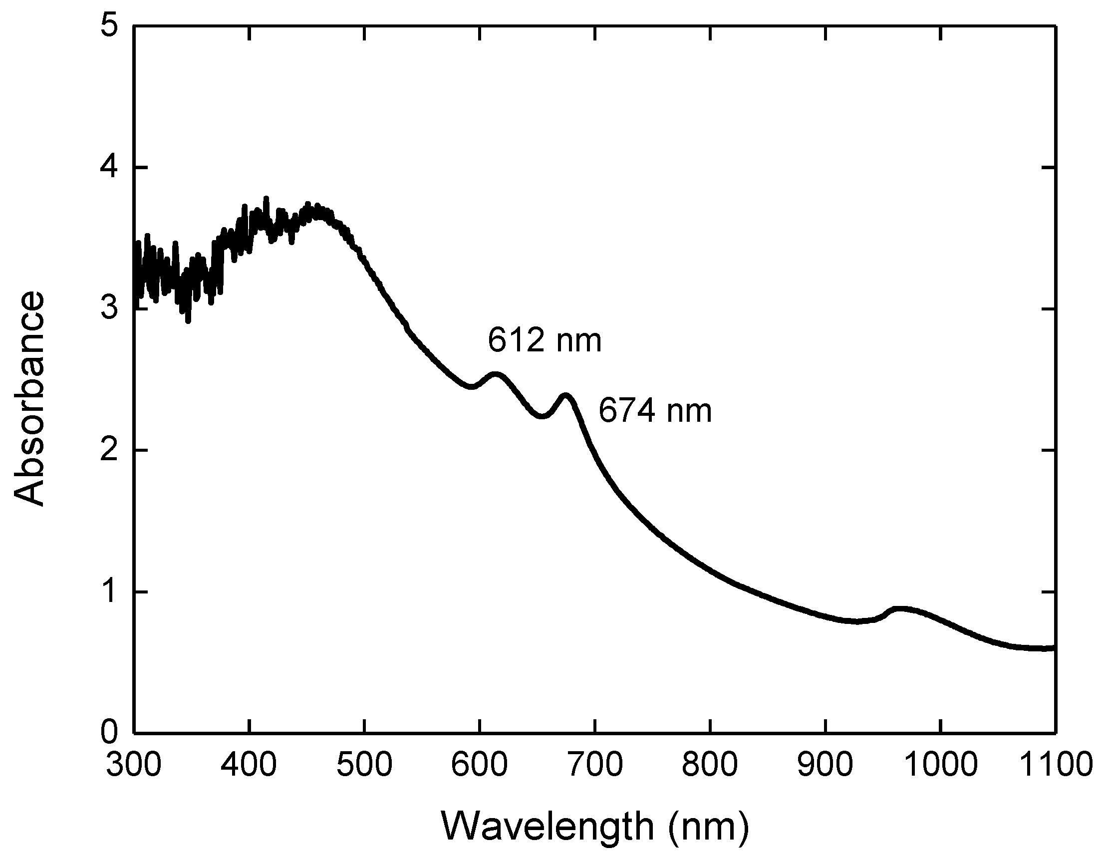
Figure 3.
Resonant Raman spectra of MoS2 modified-PA6 nanofibrous excited using a 633 nm laser.
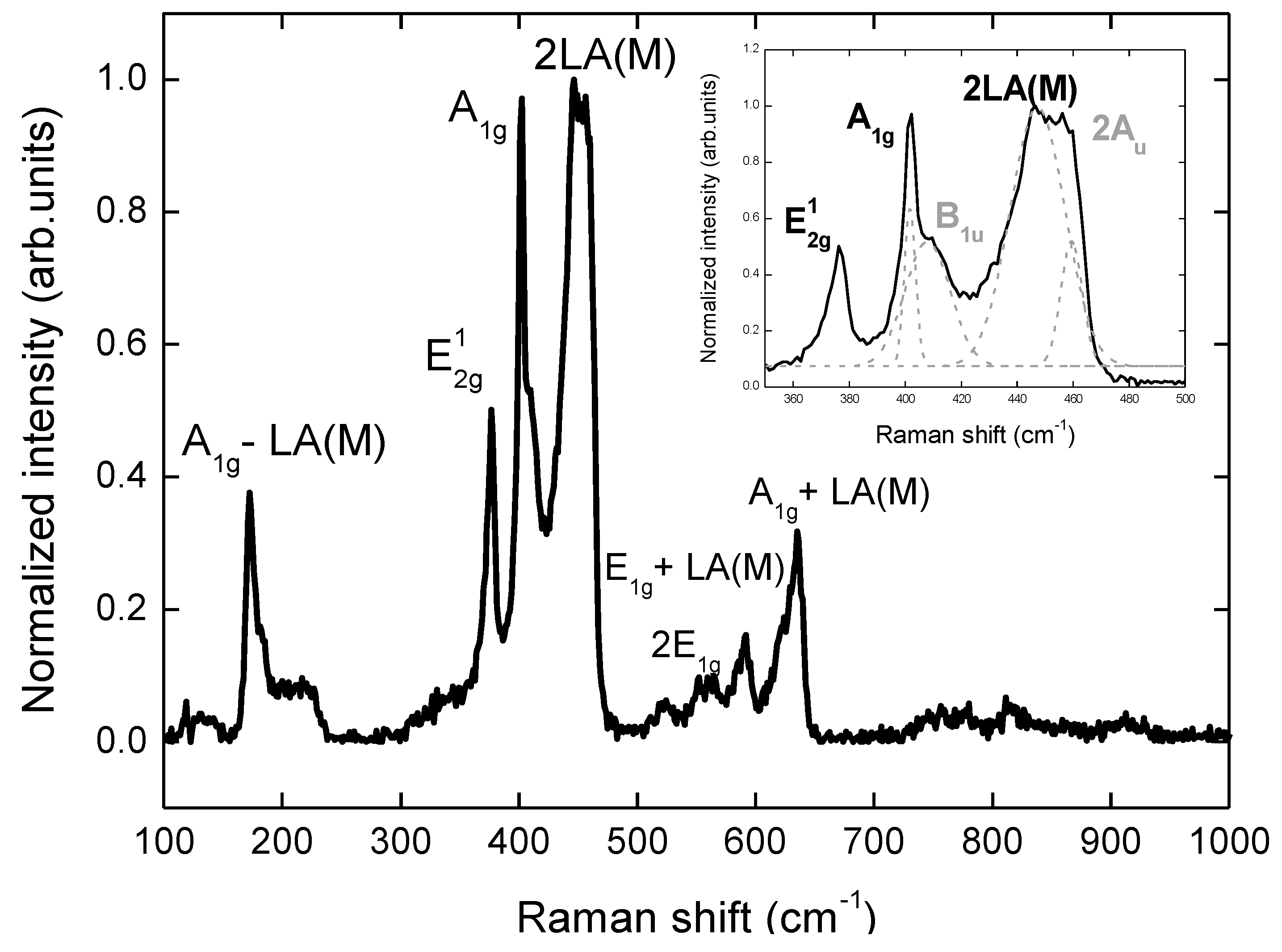
Figure 4.
Squared line width as a function of the pulse energy for 50 µm/s of translation speed. The inset shows an optical microscopy image of fs-laser micromachined lines using 25 nJ, in which the white lines represent the removed (laser-ablated) material and the black regions correspond to the remaining material.
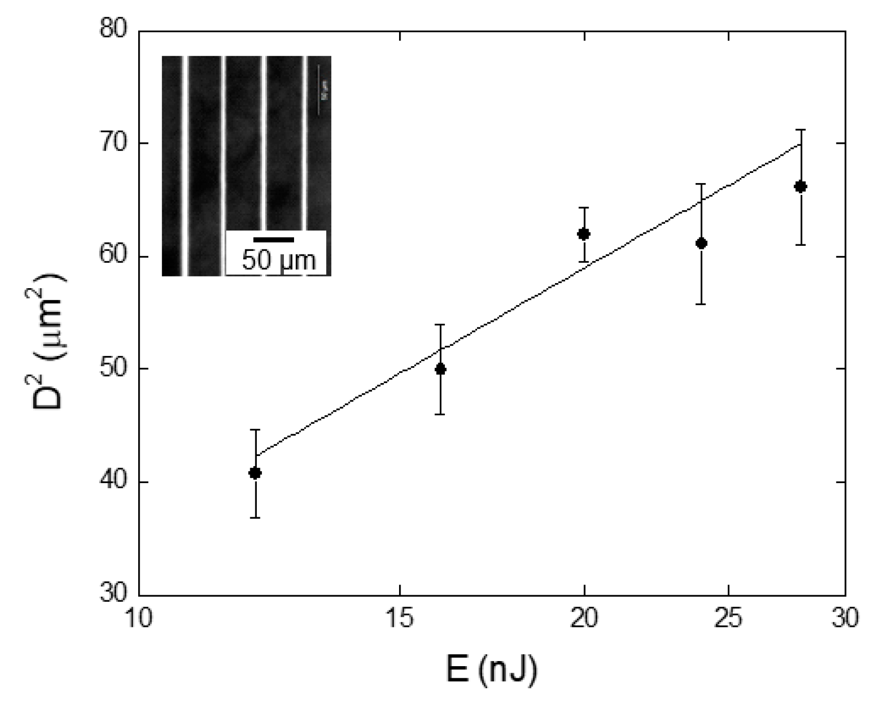
Figure 5.
SEM images of micromachined pillars with a periodicity of 40 µm (a) in the top view and (b) at a tilted angle of 45°, (c) 30 µm and (d) 20 µm obtained in the top view.
Figure 5.
SEM images of micromachined pillars with a periodicity of 40 µm (a) in the top view and (b) at a tilted angle of 45°, (c) 30 µm and (d) 20 µm obtained in the top view.
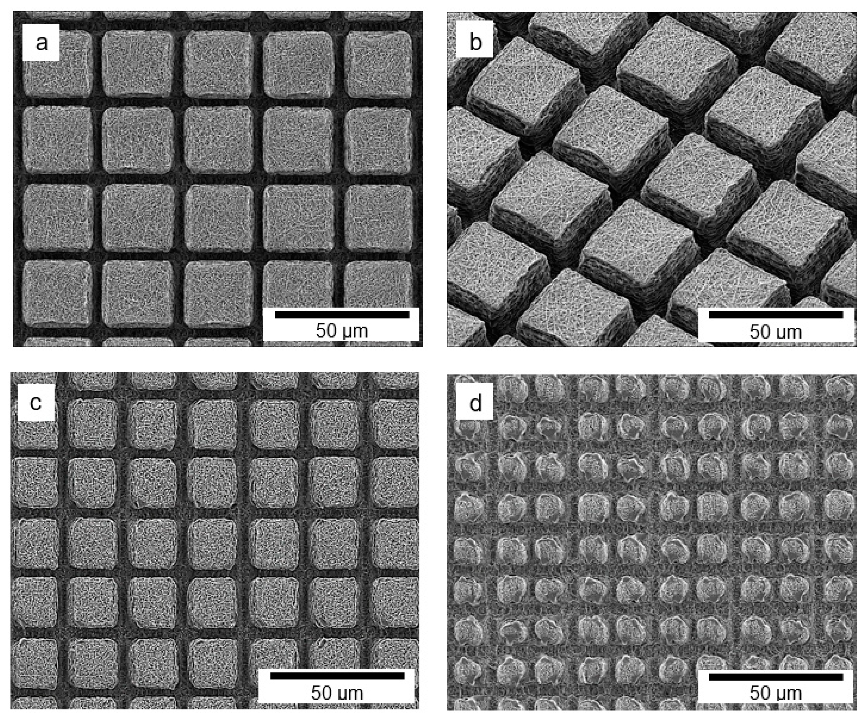
Figure 6.
Squared line width as a function of the pulse energy for 50 µm/s of translation speed. The inset shows an optical microscopic image of fs-laser micromachined lines using 5 nJ, in which the white lines represent the removed (laser–ablated) material and the gray regions correspond to the remaining material.

Figure 7.
SEM images of micromachined pillars with a periodicity of 40 µm obtained by modifying the PA6 nanofibers with MoS2 (a) before laser microfabrication (DBM) and (b) after laser microfabrication (DAM).
Figure 7.
SEM images of micromachined pillars with a periodicity of 40 µm obtained by modifying the PA6 nanofibers with MoS2 (a) before laser microfabrication (DBM) and (b) after laser microfabrication (DAM).
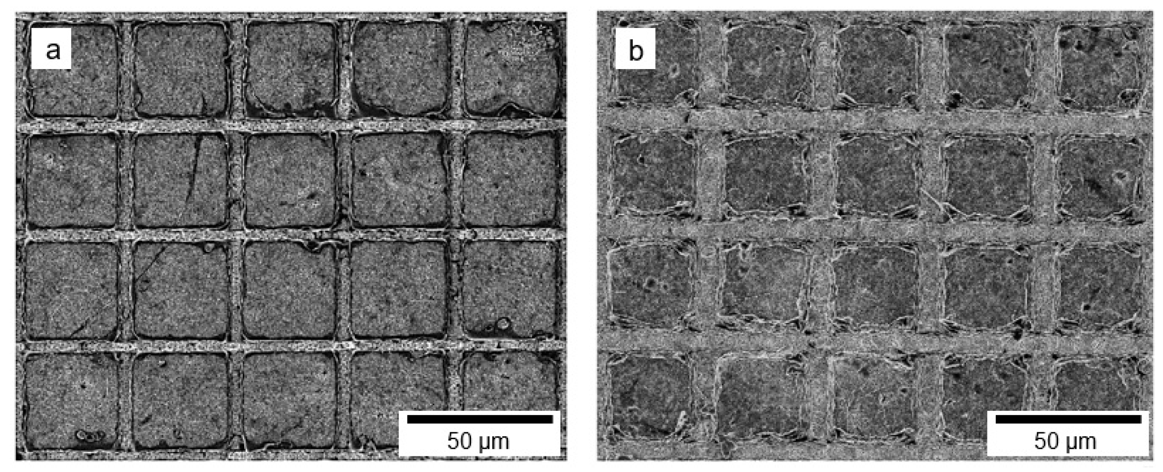
Figure 8.
(a) The energy-dispersive X-ray (EDX) spectrum, and elemental mapping of the nanofibers modified with MoS2 (b) before laser microfabrication and (c) after laser microfabrication.
Figure 8.
(a) The energy-dispersive X-ray (EDX) spectrum, and elemental mapping of the nanofibers modified with MoS2 (b) before laser microfabrication and (c) after laser microfabrication.

Figure 9.
(a) Photoluminescence emission spectrum of the PA6–MoS2 composite nanofibers at two different excitation wavelengths: the gray line at 575 nm and the black line at 639 nm. Confocal fluorescence microscope images obtained using laser excitation at 639 nm of micromachined pillars with a periodicity of 40 µm for nanofibrous membranes modified with MoS2 (b) before and (c) after laser microfabrication.

© 2019 by the authors. Licensee MDPI, Basel, Switzerland. This article is an open access article distributed under the terms and conditions of the Creative Commons Attribution (CC BY) license (http://creativecommons.org/licenses/by/4.0/).
Share and Cite
MDPI and ACS Style
Paula, K.T.; Mercante, L.A.; Schneider, R.; Correa, D.S.; Mendonca, C.R. Micropatterning MoS2/Polyamide Electrospun Nanofibrous Membranes Using Femtosecond Laser Pulses. Photonics 2019, 6, 3. https://doi.org/10.3390/photonics6010003
AMA Style
Paula KT, Mercante LA, Schneider R, Correa DS, Mendonca CR. Micropatterning MoS2/Polyamide Electrospun Nanofibrous Membranes Using Femtosecond Laser Pulses. Photonics. 2019; 6(1):3. https://doi.org/10.3390/photonics6010003
Chicago/Turabian StylePaula, Kelly T., Luiza A. Mercante, Rodrigo Schneider, Daniel S. Correa, and Cleber R. Mendonca. 2019. "Micropatterning MoS2/Polyamide Electrospun Nanofibrous Membranes Using Femtosecond Laser Pulses" Photonics 6, no. 1: 3. https://doi.org/10.3390/photonics6010003
Note that from the first issue of 2016, this journal uses article numbers instead of page numbers. See further details here.