Light–Matter Interaction of Single Quantum Emitters with Dielectric Nanostructures
by
 , , ,
, , ,
Lina Jaya Diguna
1, 
Liliana Tjahjana
2,3,
Yudi Darma
4,
Shuwen Zeng
2,5,*,
Hong Wang
2,3 and
Muhammad Danang Birowosuto
2,6,*
1
Department of Renewable Energy Engineering, Prasetiya Mulya University, Kavling Edutown I.1, Jl. BSD Raya Utama, BSD City, Tangerang 15339, Indonesia
2
CNRS International NTU THALES Research Alliances/UMI 3288 (CINTRA), Research Techno Plaza, 50 Nanyang Drive, Border X Block, Level 6, Singapore 637553, Singapore
3
School of Electrical and Electronic Engineering, Nanyang Technological University, 50 Nanyang Avenue, Singapore 639798, Singapore
4
Department of Physics, Bandung Institute of Technology, Jl. Ganesha No. 10, Bandung 40132, Indonesia
5
XLIM Research Institute, UMR 7252 CNRS/University of Limoges, 123, avenue Albert Thomas, 87060 Limoges CEDEX, France
6
Physics Research Center, the Indonesian Institute of Sciences, Puspitek, Serpong, Banten 15314, Indonesia
*
Authors to whom correspondence should be addressed.
Photonics 2018, 5(2), 14; https://doi.org/10.3390/photonics5020014
Submission received: 28 February 2018
/
Revised: 20 May 2018
/
Accepted: 11 June 2018
/
Published: 13 June 2018
Abstract
:Single quantum emitters are critical components for many future quantum information technologies. Novel active material systems have been developed and transitioned into engineering efforts at nanoscale. Here, we review recent progress of diverse quantum emitters and their optical properties, including fluorescent point defect in bulk and single nanocrystal, two-dimensional materials, and quantum dots (QDs). Remarkable progress has also been made in controlling spontaneous emission by utilizing the local density of optical states in dielectric photonic nanostructures. We focus on the enhanced light–matter interaction between the emitter and cavity, enabling the realization of efficient and fast single photon sources.
1. Introduction
Single quantum emitters play a central role in various quantum information applications, such as communication [1], computation [2], and gyroscopes [3], which require the use of single, indistinguishable photons as carriers of information and logic operators [4]. Therefore, in this field, it needs to be ascertained that the light sources can dependably produce individual photons in identical states. If an individual photon is delivered at one time, and sent toward a beam splitter, then the single photon will be either reflected or transmitted. The indistinguishability or the degree of the interference of two photons is characterized by calculating a normalized measure of two-photon interference among photons emitted from single emitters. The normalized first-order correlation function between pairs of photon, g(1), is used for quantifying the coherence between two photons, while its normalized second-order correlation function, g(2), is typically used to find the statistical character of intensity fluctuations. The observation of antibunching by means of g(2) reveals whether there is only a single photon emitter present. The parameters of interest today for single quantum emitters are the emission wavelength and accurate measurement of the g(2)(τ) function. At telecom wavelength, the reported single photon sources, so far, are at 1.5 μm wavelength, such as InAs QD in L3 photonic crystal cavity [5], at the tip of optical horn structure [6,7], in slow light mode of photonic crystal cavity [8], and in single hole defect of photonic crystal cavity [9]. In addition, telecom wavelength single photon emission can be obtained through upconversion [10]. For telecommunication application, single quantum emitters should have fast emission with a lifetime less than 1 ns. Therefore, the emission photons can be modulated at repetition rate higher than 1 GHz for maintaining high transferred secure bit rate after transmission. At the neighboring visible spectrum, the single photon emitter at visible wavelength [11] is also useful for telecommunication, such as in free space communication [12] and miniaturized quantum information circuits with available high-sensitivity and high-speed detectors [13]. Efficient single quantum emitter can be further realized through controlling their emission through the use of dielectric nanostructures. In this review, we will first discuss the types of single quantum emitters of different structures and materials. The advantages and challenges of each of the quantum emitters will be investigated, with aims for the focused emitters. Finally, we will close our discussion on how we can control the spontaneous emission of the emitters using dielectric nanostructures. We know that plasmonic metamaterials have been extensively studied for emission enhancement, but here we will focus on dielectric nanostructures, as they can provide additional phenomena, such as the emission inhibition in photonic crystals, which may shield the single photon emission from the unwanted emission channel and the strong localization in random photonic materials which may provide strong fluctuations between emission inhibition and enhancement.
2. Platforms for Realization of Single Quantum Emitters
Over the past decade, much effort has been made to engineer single quantum emitters on the basis of different platforms, in terms of different structure and material systems. Figure 1a shows the simplified experimental scheme of single photon with the inset as antibunching curve. Therefore, if a single photon delivered at one time is striking a beamsplitter, the photon will be refracted or transmitted. Observation of antibunching by means of the normalized second-order correlation function reveals whether there is only one photon present in a given time while there is no photon at zero delay, see inset in Figure 1a. However, the second order correlation function is only close to zero. The solid-state and molecular single photon source performances are limited due to the dephasing and multiphoton background emission [14], while those of the optically pumped non-linear crystals are limited by the laser-excitation linewidth [15]. The best antibunching level is hitherto reported for electrically-injected single quantum dot micropillar with g(2)(0) of 0.0028 ± 0.0012 and high extraction efficiency of 65% [16]. Figure 1b–d shows some single quantum emitters, such as the previously studied color centers in bulk three-dimensional (3D) hosts and nanocrystals, two-dimensional (2D) materials, and quantum disks embedded in nanowires. In this section, we will briefly review the available single quantum emitters and consider their photophysical properties. We will also discuss the challenges inherent to each system, and highlight new research directions that are currently being explored.
2.1. Single Quantum Dots
Various materials of quantum dots have been introduced and fabricated by different methods, such as chemical synthesis, etching from 2D nanostructures, and self-organized growth. Figure 2 shows the performance of single quantum emitters fabricated by (a) and (b) chemical synthesis, (c) and (d) etching from 2D nanostructures, (e) and (f) self-organized growth. An example of chemically synthesized QDs is chemical solution-processed colloidal quantum dots, in particular, lead chalcogenide QDs. In Figure 2a, photoluminescence (PL) spectra of PbS QDs show a strong intensity quenching and shift of emission peak about 50 nm towards shorter wavelength from a peak of 1400 nm at 4 K as temperature increases [17]. This quenching at higher temperature is accompanied by the shortening of the photoluminescence decay curves and total decay time. For single core–shell PbS/CdS nanocrystal as shown in Figure 2b, it has been confirmed that at room temperature its photoluminescence at shortwave-infrared wavelength of 1100 nm is strongly antibunched, in which the 0–time dip for the normalized second-order correlation intensity autocorrelation g(2)(0) was found to be 0.415, in contrast to those in a cluster of nanocrystals with the absence of the dip [18].
Besides lead chalcogenide colloidal nanocrystals, lead halide-based perovskite CsPbX3 (X = I, Br) QDs have also been demonstrated to have strong photon antibunching detected in the photoluminescence at room temperature, where g(2)(0) for CsPbI3 QD is 0.061 and 0.05 under continuous wave and pulsed excitations, respectively, although the photochemical stability and photocharging problems must be resolved to realize its application [19]. In colloidal QD, this strong antibunching arises from fast Auger recombination, suppressing emission from biexcitons and higher-order multiexcitons. As for quantum emitters realized by etching from 2D nanostructures, quantum emitter in the nanowire might have varied emission rates into fundamental guided mode by varying the nanowire diameter. For InAs quantum dots embedded in GaAs nanowires, the optically confined mode in nanowires with the optimal diameter was reported to enhance the emission and lead to an efficient funneling of the spontaneous emission into the guided mode [20]. Here, decreasing the wire diameter would vanish the coupling to the guided mode, and thus allow the coupling to the continuum of the radiative modes. The comparable way to control emission was also observed by Birowosuto et al. for the case of InAs quantum disks in InP nanowires having the inhibition affected by the disk diameter and thickness [21]. InAs quantum disks embedded in InP nanowires with the typical photoluminescence spectra and polarization study from single nanowires are shown in Figure 2c,d, indicating that QDs emission are polarized perpendicular to the axis of the nanowire. Here, they also investigated the inhibition at 1500 nm, about 2.5-fold smaller than that for the standing nanowire when the nanowire is placed on the higher refractive index substrate of Si.
For nanoscale patterned QD layer, as shown in Figure 2e, InAs QDs have been reported to have the complex excitons composed of exciton and biexciton with the emission at telecom wavelengths of 1556.8 nm and 1561.1 nm, and the excitation power-dependent integrated intensities exhibiting almost linear and quadratic behavior, respectively [22,23]. The structure consists of InAs QDs in InP photonic crystal (PhC) which was fabricated by metalorganic vapor phase epitaxy, electron-beam lithography and high resolution dry etching. The time-resolved photoluminescence showed exponential decay for exciton and biexciton with the time constants of τexciton = 1.6 ns [6,22,24,25,26] and τbiexciton = 1.0 ns [22], respectively, showing that the biexciton emission has faster decay time than exciton, while the second-order correlation function for the light emitted from biexciton also showed single photon characteristics [22]. The indistinguishability of photons emitted by a semiconductor quantum dots later was probed via time- and temperature-dependent two-photon interference experiments, whereas increasing temporal separation between consecutive photon emission events and temperature results in a decrease in visibility on a nanosecond time scale [27].
2.2. Fluorescent Point Defects in Bulk and Single Nanocrystal
A wide range of fluorescent point defects in bulk and single nanocrystal exist both as vacancy or impurity defects, and many of these emitters are active and even stable at room temperature, as shown in Figure 1b. The stable room-temperature operation enables rapid characterization and fast research and development cycles for material improvement. Optically active nitrogen vacancy (NV) and silicon vacancy defects are the most studied in diamond structure [28]. Nitrogen vacancy center has a non-zero electronic dipole moment causing spectral wandering proportional to the changes in the local strain and electric fields. At zero field and room temperature, the splitting of the spin states is 2.87 GHz, and it can be coupled by microwave resonance, leading to the sensor platform for measuring magnetic fields, temperature, pressure, rotation, or time [28]. The inhomogeneous strain structure in NV center can also be stabilized by using Stark effect schemes to control and offset the fluctuations [29]. Further with an interferometric method, this spectral diffusion of the zero-phonon line (ZPL) of single NV centers in diamond nanocrystals could also be optimized by using relatively high excitation powers around 20–30 μW, but clearly below the saturation level, and proper excitation energy of 2.3 eV (when deep charge traps present) [30]. Various efforts have been put on coupling NV centers to nanostructures [31]. On the other hand, silicon vacancy defects in diamond are less susceptible to local environmental fluctuation, due to their inversion symmetry. Separated silicon vacancy defects in diamond have been demonstrated to efficiently generate coherent optical photons with excellent spectra properties [32]. Recent works have also focused on color centers in the compound semiconductors. Silicon carbide (SiC) with large band gap (typically 3–4 eV) has been discovered as ultrabright single photon emitter originated from an intrinsic defect known as the carbon antisite-vacancy pair, which was created by carefully optimized electron irradiation and annealing of ultrapure SiC [33]. Wide band gap II–VI compound semiconductor ZnO (3.4 eV at room temperature) has been also considered as a candidate for single photon emitter. Single photon emission has been observed from isolated zinc vacancies in nanoparticle-derived ZnO thin films, with the radiative lifetime between 4 and 1 ns at room temperature, depending on whether the emission follows a two- or three-state mechanism [34]. The investigation of single photons from the single stable defect centers in ZnO at cryogenic temperatures also showed the line width narrowing and spectral jumps with linear dependence of jump frequency and distance on the excitation laser power, due to the fluctuation of the electrostatic environment, i.e., ionization of localized shallowed charge traps [35]. Another potential platform is rare-earth ion impurities in crystals, due to their high-Q 4f–4f optical transitions. A single photostable Pr3+ ion in yttrium aluminum garnet (YAG) nanocrystals has been detected with high contrast photon antibunching by using optical upconversion of the excited state population of the 4f–4f optical transition into ultraviolet fluorescence [36]. Although those types of emitters are stable at room temperature, they are difficult to be integrated with silicon platforms for photonics telecommunications. They are also not practical for electrical injection at single photon level, due to their atomic sizes [28].
2.3. Defects in Two-Dimensional Material
2D single quantum emitters offer the possibility to enhance the photon-extraction efficiency that is usually limited by internal reflection in the case of solid state emitters embedded in bulk materials with high refractive index. Currently, 2D materials have been reported to host single photon emission, such as transition metal dichalcogenides, in particular, tungsten diselenide (WSe2) [37,38,39,40] and hexagonal boron nitride (hBN) [41,42]. In WSe2, the quantum defects are ascribed to localized, weakly bound excitons, and often appear at the edges of 2D WSe2 flakes as emitting centers. At cryogenic temperature, the emission spectra of quantum dot-like WSe2 defects are composed of a series of the sharp emission lines that clearly reveal the photon antibunching [39,40,41,42]. When the magnetic fields apply in the Faraday configuration, the Zeeman splitting lines due to the spin–orbit coupling in one quantum emitter will be further split with larger distance along with the larger magnetic fields [39,40]. This environment sensitivity makes these WSe2 defects natural candidates for the sensing of nanoscale electromagnetic fields.
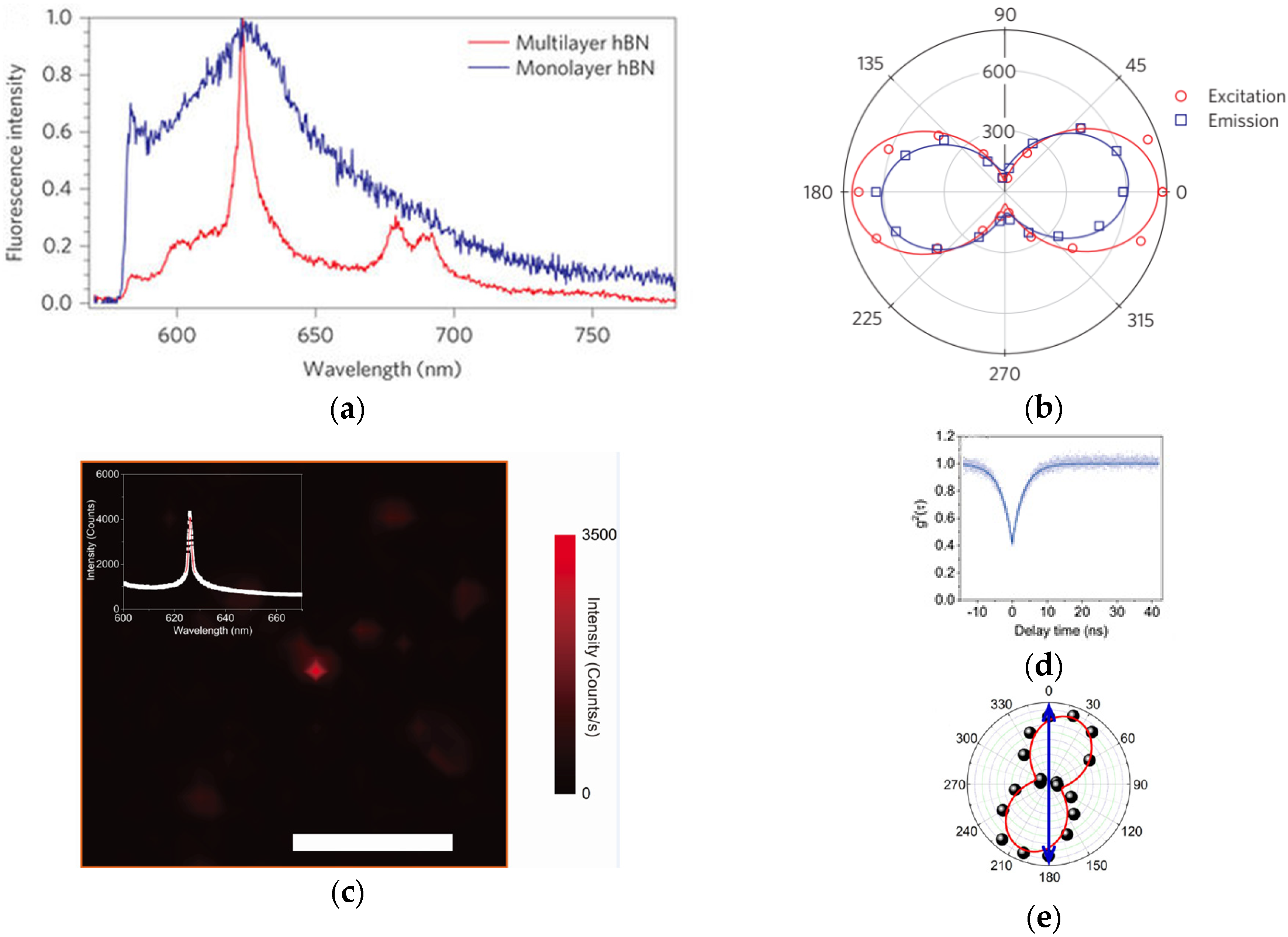
In 2D hBN, the localized vacancy-related defects have been demonstrated as the color centers. Moreover, color centers in hBN monolayer and multilayers are at the same emission wavelength which is at ~623 nm, which is attributed to the zero phonon line (ZPL) of the defect as seen in Figure 3a. The emission lines of hBN multilayers were found to be much narrower than those of monolayers, and the emitters in the multilayer hBN are photostable with the relatively high Debye–Waller factor of ~0.82, the fast excited-state lifetime of 3.1 ns, and the relatively high brightness of about 4 million counts per second in the visible spectral range at the fluorescence saturation power of 611 μW [41]. With this power, we do not need to optically pump the sample with laser beam, which potentially damages the hBN layers as the counts are similar to the brightest NV centers [28]. The similar polarizations of the excitation and the emission in Figure 3b show single linearly polarized dipole transition, indicating that the emission center consists of a single dipole. Different approaches for engineering quantum emitters in hBN layers were developed, i.e., annealing, electron beam irradiation [42], and laser ablation [43]. In the annealing method, defect diffusion and lattice relaxation occur in the as-grown hBN flakes, as annealing temperature increases in an inert environment. In the electron beam irradiation approach, the as-grown flakes were irradiated by a 15 keV, 14 nA electron beam in a low vacuum. The resulting defects exhibit a broad range of multicolor single photon emission at room temperature across the visible and near-infrared spectral ranges, with narrow line widths of ~10 nm, short excited-state lifetime and high brightness. Laser ablation technique was also recently reported to be able to engineer bright color centers in hBN monolayers and multilayers [43], where the color centers in hBN monolayers and multilayers exhibit single photon emissions with linewidths of 4.5 nm and 1.4 nm, respectively, narrower than that of ~10 nm from defects created by electron beam irradiation mentioned above; see Figure 3c,d. At cryogenic temperature, the lifetime and first-order measurements showed ultrafast spectral diffusion in hBN, whereas the photon coherence time is still less than the lifetime of the emitter in hBN, causing inhomogeneous broadening of the line [44]. Similar with fluorescent point defects in bulk and single nanocrystals, these single photon emitters are also not easy for electrical pumping. So far, only few electrically-pumped single photon emitters from WSe2 and WS2 monolayers were reported [45]. Unlike other light emitting devices, here they used heterostructures of graphene and hBN monolayers as electrodes. As for the other properties, defects in two-dimensional materials (and also nanocrystals) are better than the quantum dots, as they are very stable at room temperature, have high quantum efficiency, and large radiative emission rates [15]. Such properties will be useful if the defects are coupled with nanostructures, so that the Purcell effect will be efficient. Recently, the ultrabright NV centers of 0.25 billion photons per second was reported [46]. This is by far much larger photon counts than 1 million photons per second recorded for colloidal quantum dots in the same Purcell-coupled system [47].
Some issues still remain before the potential of single quantum emitters can be fully exploited. NV centers are usually embedded in microcrystals [28] or nanowires [48]. They are not easy to incorporate with photonic nanostructures for emission enhancements. For the first, the microcrystals will be difficult to be fit inside the smaller-than-wavelength-size cavities or antennas. Meanwhile, the nanowires with hundred-nanometer size will be too small to achieve a sufficient overlap with the confined mode in the same cavities or antennas. NV centers in diamond have shown the excellent stability at room temperature, but nanostructuring would be challenging because of the lattice rigidity [15]. In case of organic molecule system, the molecular stability is a serious issue that often severely occurred at room temperature because of many destructive photochemical processes that can be activated from the excited state by thermal fluctuations, and thus, limit the operation time at room temperature [15]. QDs are much more photostable than organic molecules, but they still face a blinking issue, in other words, the strong fluctuations of the luminescence, and require working conditions of a low temperature [15]. Furthermore, beside the emitters in this review, different quantum systems have also been proposed by doping single organic molecules into crystalline thin film, such as dibenzoterrylene molecules horizontally aligned with the plane of the thin film of anthracene, which have showed the near-infrared single photon emission stable and bright at room temperature [49,50].
For both QDs and organic molecules, nanopositioning would be difficult because their sizes are too small to be manipulated with nanotip, and this issue should also be addressed in the practical way for the system integration [51]. On the other hand, 2D materials appear more promising with the easiness for overlapping between the optical confined modes, due to their atomic thickness and for spatially manipulating due to their large lateral size.
3. Controlling Spontaneous Emission Rate through Local Density of Photonic States of Nanostructures
Spontaneous emission of an excited quantum emitter needs to be controlled for improving the performance of the nanophotonic devices, as the performance is not only an intrinsic property of the emitter itself, but it also depends on the surroundings on the nanoscale. Control of the emission rate of quantum emitters has been demonstrated in photonic media [40,52,53,54,55] including photonic crystals and disordered materials, such as shown in Figure 4. Photonic crystal with certain photonic band gap might shield the emitter from vacuum fluctuations, resulting in the inhibition of the emission inside the photonic band gap, while the presence of the cavity would enhance the emission resulting in the fast and efficient light source. Moreover, plasmonic nanostructures have been also reported for controlling the emission rate [48,49,50,51]. Compared to dielectric material with small radiative loss, the plasmonic material may give much larger spontaneous emission enhancement but with large radiative loss of plasmons [56,57,58,59].
Sprik et al. [60] proposed that the spontaneous emission of an atom placed in a dielectric is proportional to the contributions of the atomic part and the local radiative density states in surrounding part, as follows:
where is the radiative decay rate; is the dielectric permittivity; d2 is the transition dipole moment; is the local density of states. The effect of the emitter surroundings is described by the local density of states (LDOS) that represent the number of optical modes available for emission at the position of the emitter. Spontaneous emission is inhibited if the emitter is located in a position where LDOS is small, even if the total LDOS is not vanishing. In the following sections, the control of spontaneous emission through random photonic materials and photonic crystal bandgap with cavity are discussed in detail.
3.1. Random Photonic Materials
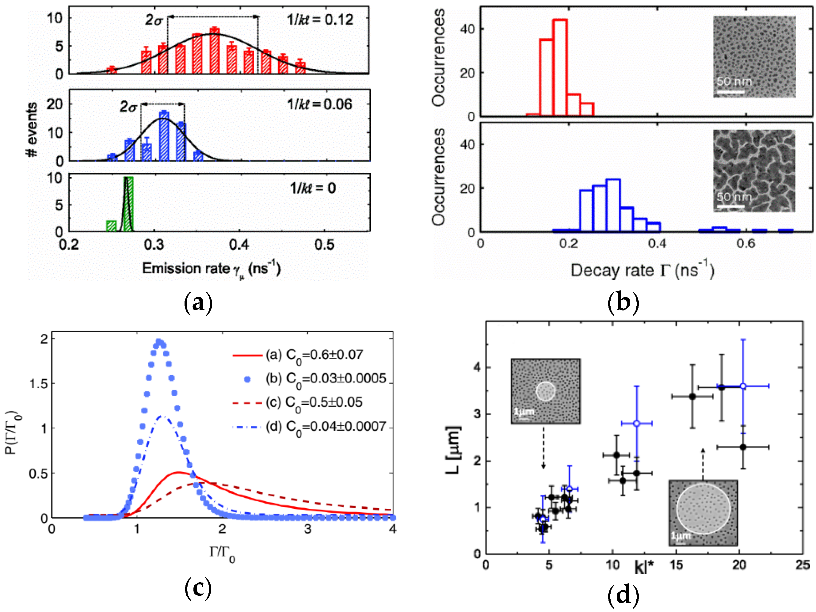
In random photonic media, the propagating light is multiply scattered, and often modeled as the random walk of photon before it leaves the media. For light with the wave number k and the transport mean free path l, the media is characterized by the scattering strength of 1/kl. The average local energy density of radiation is directly proportional to the ensemble-averaged LDOS, which counts the number of optical modes available for the emitted light. It is theoretically predicted that LDOS exhibits spatial fluctuations depending on the scattering strength near the emitter [61,62]. In an infinite random medium, the LDOS fluctuations are essentially equivalent to the C0 intensity of infinite-range correlation function. The spatial fluctuations of the LDOS in three-dimensional disordered materials have been experimentally observed for the first time by using a large number of single nanoscale emitters as internal probes of the LDOS [63], while the quantum electrodynamic (QED) experiments between disordered modes and the emitters in two-dimensional system have been demonstrated around the same time by Sapienza et al. [53]. Here, the time-resolved emission was measured for the single fluorescent nanosphere embedded deep inside random media with scattering lengths 1/kl up to 0.12 for ZnO random photonic media, as shown in Figure 5a. The time-resolved fluorescence for different single fluorescent nanospheres in random photonic medium at the same depth yield different non-exponential decay curves, while those in a nonscattering layer show the exponential decay with the same time constant. The observed nonexponential decay is attributed to the strong dependence of emission rate on dipole orientation demonstrating the spatial fluctuations of LDOS. The lognormal distribution of the emission rate in random medium widens as the scattering strength increases. This agrees with the theoretical single-sphere-scatterer model, in which the nearest scatterer dominates the LDOS fluctuations. The variance of the emission intensities provides an upper bound to the distribution of the emission rates, which is consistent with the contribution of C0 on LDOS fluctuations. Furthermore, the fluctuation of LDOS has also been used to probe the surface plasmon localization on disordered metal films [64]. As shown in Figure 5b, when the gold nanoparticle filling fraction increases, the fluorescent decay rate distribution of fluorescent polystyrene beads broadens, and the average value increases. This change in the measured spontaneous decay rate of the fluorescent nanosources on disordered gold films are attributed to the changes in the LDOS reflecting changes of the structure of the electromagnetic modes, in which the higher gold filling fraction exhibits larger spatial fluctuations with a maximum in a regime where fractal clusters dominate the film surface. These large fluctuations are a signature of surface-plasmon localization on the nanometer scale.
The statistics of LDOS has been studied by Purcell effect for nanosized emitters buried in a 3D disordered dielectric medium through fluorescence decay rates of nanosized light emitter [65]. The long-tailed and non-Gaussian behavior with large decay rates are attributed to strong localizations of the LDOS induced by the full near-field multiple-scattering. The further observed nonuniversality of LDOS distributions for systems with the same scattering strength, but different microscopic properties of C0 speckle correlation of the intensity emitted by a point source in Figure 5c shows that the scattering strength is not the single parameter driving the statistical distribution. This makes LDOS distribution a valuable quantity for sensing or imaging the microscopic structure of complex media. On the other hand, LDOS statistics has also been probed for QDs embedded in dielectric planar waveguides using a near-field hyperspectral imaging technique based on the proportionality of the intensity of the light emitted at a frequency to LDOS when the quantum emitter is subjected to a continuous excitation [66]. Different mechanisms driving the fluctuations of the LDOS in disordered photonic systems were observed, whereas the short- and long-range frequency correlations of LDOS are differently controlled by multiple and single scattering processes, respectively, that can be manipulated independently to some extent. Furthermore, due the losses of energy out of the sample plane resulting in a finite photon lifetime, the infinitely extended 2D material behaves as if it is of finite extent L in which this characteristic length scale shrinks with increasing disorder, as shown in Figure 5d. In general, by designing the statistics of scatter sizes in random photonic materials, we may obtain strong localization which may result in spatially-controlled emission rate variations that can be coupled with quantum emitter for a tunable single photon source [53].
3.2. Photonic Crystal (PhC) Cavity
Spontaneous emission by an excited atom located in the periodic structure has been considered to proceed in two ways, either the photon emission in the allowed band or transition of excited atom into a relatively long-lived state [67]. For 3D lattice of ordered-dielectric spheres with the large lattice constants, the diffraction of low energy photons, such as UV, was reportedly attributed to Bragg reflection [68,69]. In 1987, Yablonovitch has proposed the inhibition of spontaneous emission, due to the electromagnetic band gap controlled by the spatial periodic structure in dielectric materials with sufficiently large refractive index difference [70]. With moderate disorders, the strong localization of photons may occur near the edge of band gap [71]. Usually, photonic crystals were used to enhance spontaneous emission [41,52,72,73,74,75,76,77] and optimize the stimulated emission of the laser [78,79,80]. These periodic structures have also been introduced in photovoltaic application, i.e., QD-sensitized solar cells, with remarkable increase of energy conversion efficiency [81,82,83].
For the emission interacting with the confined cavity mode of the photonic crystal, if the position is overlap with the antinode and there is matching frequency with the cavity, the emission rate would be enhanced, resulting in the faster decay times [72]. Photonic crystal with band gap inhibition shielding from the vacuum fluctuation, is a good platform for strong enhancement from the cavity (Purcell) with
where Fp is cavity Purcell factor, λcav/n is the resonance wavelength in the material surrounding the emitter, Q and Vmode are the quality factor and mode volume of the cavity, respectively. Different structure types of PhC cavity-controlled spontaneous emission are quantum wells (QWs) inside the cavity of photonic crystals, single QD inside the cavity of photonic crystal, and movable cavity with QD-nanowire (NW) with the emission in telecom wavelengths. In the first type, the light emission from InGaAsP QW layers in the center of stacked GaAs striped layers of “woodpile” photonic crystal was suppressed in the photonic crystal regions, whereas cavity modes were successfully observed at the point defects artificially formed in the light-emitting layer [73].
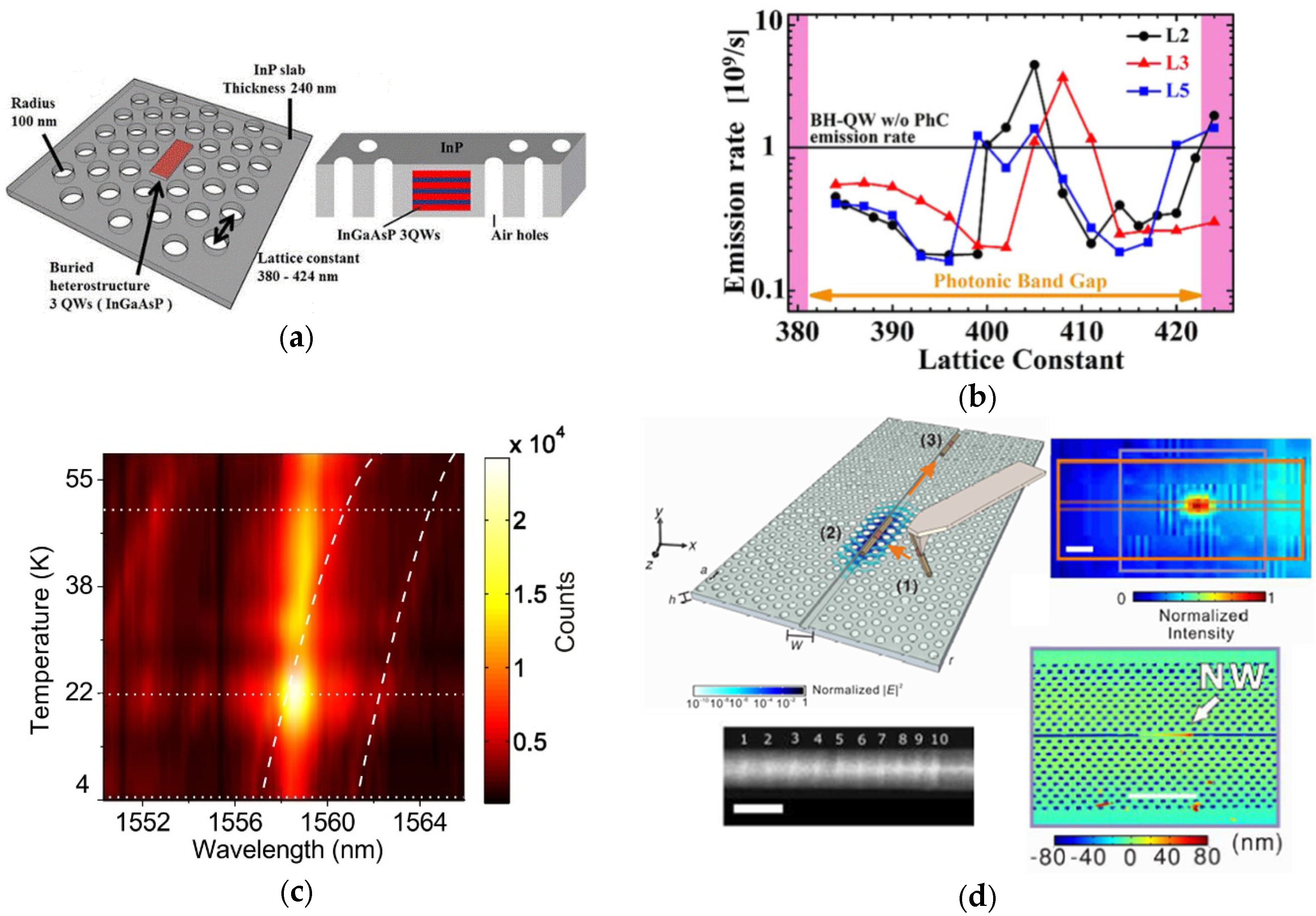
Moreover, as shown in Figure 6a, Takiguchi et al. has studied the spontaneous emission control in a buried-heterostructure (BH) photonic crystal, in which multiple InGaAsP QWs are embedded in InP PhC cavities consisting of missing air holes with end-hole shifting [74]. By varying the PhC lattice constant, the on- and off-resonant conditions show the emission lifetime to become faster, 3.8 times and lower 7.5 times, respectively, than the same-sized QW without PhC structure. These indicate Purcell enhancement and the photonic band gap (PBG) suppressing spontaneous emission. This means that the emission rate can be controlled by a factor of 30 between the on- and off-resonant conditions. As shown in Figure 6b, the emission rates from BH-QW-PhC cavities at lattice constant of around 380 and 420 nm slightly increase, because the emission wavelength is close to the band gap, noticeable especially on the long-wavelength side. Further examination on Q-factor dependence shows that the emission rate increases proportionally to the ratio of Q-factor and mode volume (Q/V), proving that the observed emission rate enhancement is due to the Purcell effect. This embedded QW-PhC design realizes strong carrier confinement, low non-radiative recombination, and high spontaneous emission coupling efficiency. This QW-PhC cavity with Q values of a few thousand was recently reported to be able to achieve lasing characteristics of high-β (spontaneous emission coupling factor) by using the finite-difference time-domain method if the cavities have only one mode in the emission spectra of the multiple QW [78]. The measurements of emission lifetime, the photon correlation, and the detuning dependence of β using several different lattice constant cavities imply that these QW-PhC nanocavity lasers are close to achieving the theoretically predicted thresholdless transition.
For single QD coupled to the cavity of photonic crystal, a very fast single photon source has been demonstrated in the 1550 nm telecom band, which is achieved by a large Purcell enhancement resulting from the coupling of a single InAs quantum dot and an InP photonic crystal cavity [39]. As shown in Figure 6c, the photoluminescent intensity of QD cavity at 22 K is 6 times larger than that of at 4 K. At the resonance, the spontaneous emission rate originated from biexciton transition was enhanced by a factor of 5, resulting in a fast emission lifetime of 0.2 ns. This emission was also demonstrated to exhibit an enhanced antibunching dip. The influence of multiple excitons on the photon emission properties of a QD-cavity system has been modeled via master equation for the density matrix, in which the small cavity-biexciton detuning yields the significant Purcell effect and the high probability of single photon characteristics of the exciton emission, and vice versa [84].
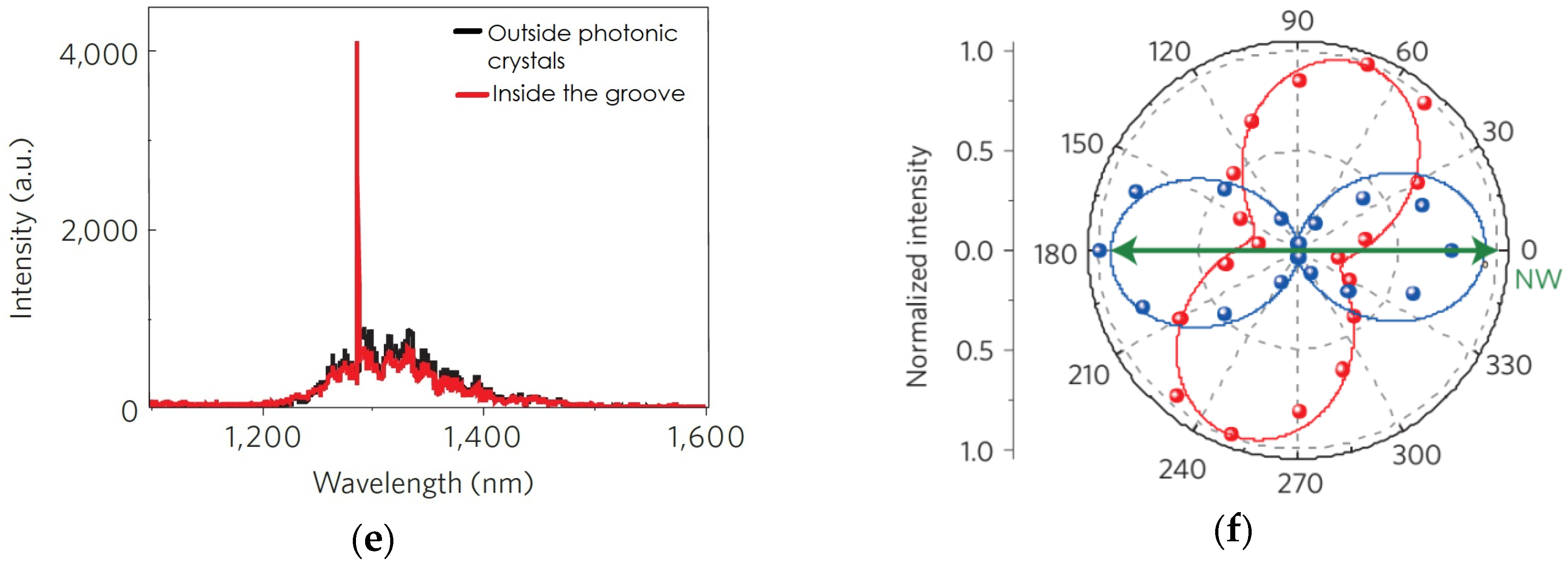
Recently, a movable hybrid cavity and emitter in a photonic crystal and NWs, as shown in Figure 6d, has been introduced by placing a single III–V semiconductor nanowire with a diameter of under 100 nm in grooved waveguide in a Si photonic crystal, by means of nanoprobe manipulation [51]. Here, the spontaneous emission of the quantum discs inside the single NW was used to probe the cavity formation by comparing the PL spectra and the emission polarization of the NW on a bare silicon-on-insulator (SOI), and inside the groove, as shown in Figure 6e,f, respectively. The PL spectrum (black lines) for a single NW outside the photonic crystal on a bare SOI exhibits peaks between 1200–1500 nm, while that of the NW inside the groove (red lines) shows a distinctive peak at 1286 nm, which is highly localized at exactly the position of the manipulated NW. The emission polarization of the NW inside the grooved waveguide was found to be almost perpendicular to the NW, and mostly matches the expected polarization for the cavity mode as shown in Figure 6d. Very fast spontaneous emission as short as 91 ps was observed from nanowires accelerated by the strong Purcell enhancement in nanocavities, which proves that very strong light confinement can be achieved. Furthermore, this system enables one to move the nanocavity anywhere along the waveguide, offering large tuning capabilities, providing a significant degree of flexibility in integrated photonics, and permitting the addition and displacement of various functionalities of III–V nanocavity devices in Si photonic circuits.
4. Conclusions
Single quantum emitters have attracted a great interest and importance for the development of new light sources, such as single photon sources for nanophotonic devices in the emerging field of quantum information processing. Various single photon emitter systems and their unique properties have been discussed, such as point defect in bulk and single nanocrystal, two-dimensional materials, and quantum dots. The use of the local density of optical states in photonic nanostructures, such as disordered photonic media and photonic crystal, has been further revealed as a remarkable approach in enhancing the light–matter interaction of single quantum emitters, resulting in the controlled spontaneous emission. In future applications of quantum information and optics, these quantum emitter-embedded dielectric nanostructures are promising to generate entanglement and quantum state transfer between two distant NV centers [85,86] and lasing in high β-microcavities [87,88]. Although many improvements in single-quantum emitters have been achieved, engineering efforts towards scalable system in real application are still challenging issues to be solved.
Acknowledgments
The authors acknowledge the financial supports from Prasetiya Mulya University, Indonesia Toray Science Foundation and Ministry of Education Singapore (MOE2016-T2-1-052). This project has received funding from the European Union’s Horizon 2020 research and innovation programme under the Marie Sklodowska-Curie grant agreement No 798916.
Conflicts of Interest
The authors declare no conflict of interest.
References
- Hu, J.-Y.; Yu, B.; Jing, M.-Y.; Xiao, L.-T.; Jia, S.-T.; Qin, G.-Q.; Long, G.-L. Experimental quantum secure direct communication with single photons. Light Sci. Appl. 2016, 5, e16144. [Google Scholar] [CrossRef]
- Knill, E.; Laflamme, R.; Milburn, G.J. A scheme for efficient quantum computation with linear optics. Nature 2001, 409, 46–52. [Google Scholar] [CrossRef] [PubMed]
- Bertocchi, G.; Alibart, O.; Ostrowsky, D.B.; Tanzilli, S.; Baldi, P. Single-photon Sagnac interferometer. J. Phys. B At. Mol. Opt. Phys. 2006, 39, 1011–1016. [Google Scholar] [CrossRef] [Green Version]
- Aharonovich, I.; Englund, D.; Toth, M. Solid-state single-photon emitters. Nat. Photonics 2016, 10, 631–641. [Google Scholar] [CrossRef]
- Iwamoto, S.; Tatebayashi, J.; Fukuda, T.; Nakaoka, T.; Ishida, S.; Arakawa, Y. Observation of 1.55 μm light emission from InAs quantum dots in photonic crystal microcavity. Jpn. J. Appl. Phys. 2005, 44, 2579–2583. [Google Scholar] [CrossRef]
- Takemoto, K.; Takatsu, M.; Hirose, S.; Yokoyama, N.; Sakuma, Y.; Usuki, T.; Miyazawa, T.; Arakawa, Y. An optical horn structure for single-photon source using quantum dots at telecommunication wavelength. J. Appl. Phys. 2007, 101, 081720. [Google Scholar] [CrossRef]
- Takemoto, K.; Nambu, Y.; Miyazawa, T.; Wakui, K.; Hirose, S.; Usuki, T.; Takatsu, M.; Yoshino, K.; Tomita, A.; Yorozu, S.; et al. Transmission experiment of quantum keys over 50 km using high-performance quantum-dot single-photon source at 1.5 μm wavelength. Appl. Phys. Exp. 2010, 3, 092802. [Google Scholar] [CrossRef]
- Chauvin, N.; Zinoni, C.; Francardi, M.; Gerardino, A.; Balet, L.; Alloing, B.; Li, L.H.; Fiore, A. Controlling the charge environment of single quantum dots in a photonic-crystal cavity. Phys. Rev. B 2009, 80, 241306. [Google Scholar] [CrossRef]
- Dalacu, D.; Mnaymneh, K.; Sazonova, V.; Poole, P.J.; Aers, G.C.; Lapointe, J.; Cheriton, R.; Thorpe, A.J.S.; Williams, R. Deterministic emitter-cavity coupling using a single-site controlled quantum dot. Phys. Rev. B 2010, 82, 033301. [Google Scholar] [CrossRef]
- Rakher, M.T.; Ma, L.; Slattery, O.; Tang, X.; Srinivasan, K. Quantum transduction of telecommunications-band single photons from a quantum dot by frequency upconversion. Nat. Photonics 2010, 4, 786–791. [Google Scholar] [CrossRef]
- Lohrmann, A.; Iwamoto, N.; Bodrog, Z.; Castelletto, S.; Ohshima, T.; Karle, T.J.; Gali, A.; Prawer, S.; McCallum, J.C.; Johnson, B.C. Single-photon emitter diode in silicon carbide. Nat. Commun. 2015, 6, 7783. [Google Scholar] [CrossRef] [PubMed]
- Rarity, J.G.; Tapster, P.R.; Gorman, P.M. Secure free-space key exchange to 1.9 km and beyond. J. Mod. Opt. 2001, 48, 1887–1901. [Google Scholar] [CrossRef]
- Hadfield, R.H. Single-photon detectors for optical quantum information applications. Nat. Photonics 2009, 3, 696–705. [Google Scholar] [CrossRef]
- Ates, S.; Agha, I.; Gulinatti, A.; Rech, I.; Badolato, A.; Srinivasan, K. Improving the performance of bright quantum dot single photon sources using temporal filtering via amplitude modulation. Sci. Rep. 2013, 3, 1397. [Google Scholar] [CrossRef] [PubMed] [Green Version]
- Lounis, B.; Orrit, M. Single-photon sources. Rep. Prog. Phys. 2005, 68, 1129–1179. [Google Scholar] [CrossRef]
- Somachi, N.; Giesz, V.; Santis, L.D.; Loredo, J.C.; Almeida, M.P.; Hornecker, G.; Portalupi, S.L.; Grange, T.; Antón, C.; Demory, J.; et al. Near-optimal single-photon sources in the solid state. Nat. Photonics 2016, 10, 340–345. [Google Scholar] [CrossRef] [Green Version]
- Birowosuto, M.B.; Takiguchi, M.; Olivier, A.; Tobing, L.Y.; Kuramochi, E.; Yokoo, A.; Hong, W.; Notomi, M. Temperature-dependent spontaneous emission of PbS quantum dots inside photonic nanostructures at telecommunication wavelength. Opt. Commun. 2017, 383, 555–560. [Google Scholar] [CrossRef]
- Correa, R.E.; Dauler, E.A.; Nair, G.; Pan, S.H.; Rosenberg, D.; Kerman, A.J.; Molnar, R.J.; Hu, X.; Marsili, F.; Anant, V.; et al. Single Photon Counting from Individual Nanocrystals in the Infrared. Nano Lett. 2012, 12, 2953–2958. [Google Scholar] [CrossRef] [PubMed]
- Park, Y.-S.; Guo, S.; Marakov, N.S.; Klimov, V.I. Room Temperature Single-Photon Emission from Individual Perovskite Quantum Dots. ACS Nano 2015, 9, 10386–10393. [Google Scholar] [CrossRef] [PubMed]
- Bleuse, J.; Claudon, J.; Creasey, M.; Malik, N.S.; Gérard, J.-M. Inhibition, Enhancement, and Control of Spontaneous Emission in Photonic Nanowires. Phys. Rev. Lett. 2011, 106, 103601. [Google Scholar] [CrossRef] [PubMed]
- Birowosuto, M.D.; Zhang, G.; Yokoo, A.; Takiguchi, M.; Notomi, M. Spontaneous emission inhibition of telecom-band quantum disks inside single nanowire on different substrates. Opt. Express 2014, 22, 11713–11726. [Google Scholar] [CrossRef] [PubMed]
- Birowosuto, M.D.; Sumikura, H.; Matsuo, S.; Taniyama, H.; van Veldhoven, P.J.; Nötzel, R.; Notomi, M. Fast-Purcell-enhanced single photon source in 1550-nm telecom band from a resonant quantum dot-cavity coupling. Sci. Rep. 2012, 2, 231. [Google Scholar] [CrossRef] [PubMed]
- Cade, N.I.; Gotoh, H.; Kamada, H.; Nakano, H.; Anantathanasarn, S.; Nötzel, R. Optical characteristics of single InAs/InAsP/InP(100) quantum dots emitting at 1.55 nm. Appl. Phys. Lett. 2006, 89, 181113. [Google Scholar] [CrossRef]
- Dusanowski, Ł.; Syperek, M.; Rudno-Rudziński, W.; Mrowiński, P.; Sȩk, G.; Misiewicz, J.; Somers, A.; Reithmaier, J.P.; Höfling, S.; Forchel, A. Exciton and biexciton dynamics in single self-assembled InAs/InGaAlAs/InP quantum dash emitting near 1.55 μm. Appl. Phys. Lett. 2013, 103, 253113. [Google Scholar] [CrossRef]
- Miyazawa, T.; Nakaoka, T.; Usuki, T.; Arakawa, Y.; Takemoto, K.; Hirose, S.; Okumura, S.; Takatsu, M.; Yokoyama, N. Exciton dynamics in current-injected single quantum dot at 1.55 mm. Appl. Phys. Lett. 2008, 92, 161104. [Google Scholar] [CrossRef]
- Dorenbos, S.N.; Sasakura, H.; van Kouwen, M.P.; Akopian, N.; Adachi, S.; Namekata, N.; Jo, M.; Motohisa, J.; Kobayashi, Y.; Tomioka, K.; et al. Position controlled nanowires for infrared single photon emission. Appl. Phys. Lett. 2010, 97, 171106. [Google Scholar] [CrossRef] [Green Version]
- Thoma, A.; Schnauber, P.; Gschrey, M.; Seifried, M.; Wolters, J.; Schulze, J.H.; Strittmatter, A.; Rodt, S.; Carmele, A.; Knorr, A.; et al. Exploring dephasing of a solid-state quantum emitter via time- and temperature-dependent hong-ou-mandel experiments. Phys. Rev. Lett. 2016, 116, 033601. [Google Scholar] [CrossRef] [PubMed]
- Aharonovich, I.; Neu, E. Diamond Nanophotonics. Adv. Opt. Mater. 2014, 2, 911–928. [Google Scholar] [CrossRef] [Green Version]
- Acosta, V.M.; Santori, C.; Faraon, A.; Juang, Z.; Fu, K.-M.C.; Stacey, A.; Simpson, D.A.; Ganesan, K.; Tomljenovic-Hanic, S.; Greentree, A.D.; et al. Dynamic stabilization of the optical resonances of single nitrogen-vacancy centers in diamond. Phys. Rev. Lett. 2012, 108, 206401. [Google Scholar] [CrossRef] [PubMed]
- Wolters, J.; Sadzak, N.; Schell, A.W.; Schröder, T.; Benson, O. Measurement of the ultrafast spectral diffusion of the optical transition of nitrogen vacancy centers in nano-size diamond using correlation interferometry. Phys. Rev. Lett. 2013, 110, 027401. [Google Scholar] [CrossRef] [PubMed]
- Wolters, J. Integrated Quantum Hybrid Systems, 1st ed.; Pan Stanford: New York, NY, USA, 2015. [Google Scholar]
- Sipahigil, A.; Jahnke, K.D.; Rogers, L.J.; Teraji, T.; Isoya, J.; Zibrov, A.S.; Jelezko, F.; Lukin, M.D. Indistinguishable photons from separated silicon-vacancy centers in diamond. Phys. Rev. Lett. 2014, 113, 113602. [Google Scholar] [CrossRef] [PubMed]
- Castelletto, S.; Johnson, B.C.; Ivády, V.; Umeda, T.; Gali, A.; Ohshima, T. A silicon carbide room-temperature single-photon source. Nat. Mater. 2013, 13, 151–156. [Google Scholar] [CrossRef] [PubMed]
- Morfa, A.J.; Gibson, B.C.; Karg, M.; Karle, T.J.; Greentree, A.D.; Mulvaney, P.; Tomljenovic-Hanic, S. Single-photon emission and quantum characterization of zinc oxide defects. Nano Lett. 2012, 12, 949–954. [Google Scholar] [CrossRef] [PubMed]
- Neitzke, O.; Morfa, A.; Wolters, J.; Schell, A.W.; Kewes, G.; Benson, O. Investigation of line width narrowing and spectral jumps of single stable defect centers in ZnO at cryogenic temperature. Nano Lett. 2015, 15, 3024–3029. [Google Scholar] [CrossRef] [PubMed]
- Kolesov, R.; Xia, K.; Reuter, R.; Stöhr, R.; Zappe, A.; Meijer, J.; Hemmer, P.R.; Wrachtrup, J. Optical detection of a single rare-earth ion in a crystal. Nat. Commun. 2012, 3, 1029. [Google Scholar] [CrossRef] [PubMed] [Green Version]
- Chakraborty, C.; Kinnischtzke, L.; Goodfellow, K.M.; Beams, R.; Vamivakas, A.N. Voltage-controlled quantum light from an atomically thin semiconductor. Nat. Nanotechnol. 2015, 10, 507–511. [Google Scholar] [CrossRef] [PubMed]
- He, Y.-M.; Clark, G.; Schaibley, J.R.; He, Y.; Chen, M.-C.; Wei, Y.-J.; Ding, X.; Zhang, Q.; Yao, W.; Xu, X.; et al. Single quantum emitters in monolayer semiconductors. Nat. Nanotechnol. 2015, 10, 497–502. [Google Scholar] [CrossRef] [PubMed] [Green Version]
- Koperski, M.; Nogajewski, K.; Arora, A.; Cherkez, V.; Mallet, P.; Veuillen, J.-Y.; Marcus, J.; Kossacki, P.; Potemski, M. Single photon emitters in exfoliated WSe2 structures. Nat. Nanotechnol. 2015, 10, 503–506. [Google Scholar] [CrossRef] [PubMed]
- Srivastava, A.; Sidler, M.; Allain, A.V.; Lembke, D.S.; Kis, A.; Imamoğlu, A. Optically active quantum dots in monolayer WSe2. Nat. Nanotechnol. 2015, 10, 491–496. [Google Scholar] [CrossRef] [PubMed]
- Tran, T.T.; Bray, K.; Ford, M.J.; Toth, M.; Aharonovich, I. Quantum emission from hexagonal boron nitride monolayers. Nat. Nanotechnol. 2016, 11, 37–41. [Google Scholar] [CrossRef] [PubMed]
- Tran, T.T.; Elbadawi, C.; Totonjian, D.; Lobo, C.J.; Grosso, G.; Moon, H.; Englund, D.R.; Ford, M.J.; Aharonovich, I.; Toth, M. Robust Multicolor Single Photon Emission from Point Defects in Hexagonal Boron Nitride. ACS Nano 2016, 10, 7331–7338. [Google Scholar] [CrossRef] [PubMed] [Green Version]
- Hou, S.; Birowosuto, M.D.; Umar, S.; Anicet, M.A.; Tay, R.Y.; Coquet, P.; Tay, B.K.; Wang, H.; Teo, H.T. Localized emission from laser-irradiated defects in two-dimensional hexagonal boron nitride. 2D Mater. 2018, 5, 015010. [Google Scholar] [CrossRef]
- Sontheimer, B.; Braun, M.; Nikolay, N.; Sadzak, N.; Aharonovich, I.; Benson, O. Photodynamics of quantum emitters in hexagonal boron nitride revealed by low-temperature spectroscopy. Phys. Rev. B 2017, 96, 121202. [Google Scholar] [CrossRef]
- Palacios-Berraquero, C.; Barbone, M.; Kara, D.M.; Chen, X.; Goykhman, I.; Yoon, D.; Ott, A.K.; Beitner, J.; Watanabe, K.; Taniguchi, T.; et al. Atomically thin quantum light-emitting diodes. Nat. Commun. 2016, 7, 12978. [Google Scholar] [CrossRef] [PubMed] [Green Version]
- Bogdanov, S.; Shalaginov, M.Y.; Lagutchev, A.; Chiang, C.-C.; Shah, D.; Baburin, A.S.; Ryzhikov, I.A.; Rodionov, I.A.; Boltasseva, A.; Shalaev, V.M. Ultrabright room-temperature single-photon emission from nanodiamond nitrogen-vacancy centers with sub-nanosecond excited-state lifetime. arXiv 2017, arXiv:1711.09481. [Google Scholar]
- Hoang, T.B.; Gleb, M.; Akselrod, G.M.; Mikkelsen, M.H. Ultrafast Room-Temperature Single Photon Emission from Quantum Dots Coupled to Plasmonic Nanocavities. Nano Lett. 2016, 16, 270–275. [Google Scholar] [CrossRef] [PubMed]
- Babinec, T.M.; Hausmann, B.J.M.; Khan, M.; Zhang, Y.; Maze, J.R.; Hemmer, P.R.; Lončar, M. A diamond nanowire single-photon source. Nat. Nanotechnol. 2010, 5, 195–199. [Google Scholar] [CrossRef] [PubMed] [Green Version]
- Toninelli, C.; Early, K.; Bremi, J.; Renn, A.; Götzinger, S.; Sandoghdar, V. Near-infrared single-photons from aligned molecules in ultrathin crystalline films at room temperature. Opt. Express 2010, 18, 6577–6582. [Google Scholar] [CrossRef] [PubMed]
- Kewes, G.; Schoengen, M.; Neitzke, O.; Lombardi, P.; Schönfeld, R.-S.; Mazzamuto, G.; Schell, A.W.; Probst, J.; Wolters, J.; Löchel, B.; et al. A realistic fabrication and design concept for quantum gates based on single emitters integrated in plasmonic-dielectric waveguide structures. Sci. Rep. 2016, 6, 28877. [Google Scholar] [CrossRef] [PubMed] [Green Version]
- Birowosuto, M.D.; Yokoo, A.; Zhang, G.; Tateno, K.; Kuramochi, E.; Takiguchi, M.; Notomi, M. Movable high-Q nanoresonators realized by semiconductor nanowires on a Si photonic crystal platform. Nat. Mater. 2014, 13, 279–285. [Google Scholar] [CrossRef] [PubMed]
- Lodahl, P.; van Driel, A.F.; Nikolaev, I.S.; Irman, A.; Overgaag, K.; Vanmaekelbergh, D.; Vos, W.L. Controlling the dynamics of spontaneous emission from quantum dots by photonic crystals. Nature 2004, 430, 654–657. [Google Scholar] [CrossRef] [PubMed] [Green Version]
- Sapienza, L.; Thyrrestrup, H.; Stobbe, S.; Gracia, P.D.; Smolka, S.; Lodahl, P. Cavity Quantum Electrodynamics with Anderson-Localized Modes. Science 2010, 327, 1352–1355. [Google Scholar] [CrossRef] [PubMed] [Green Version]
- Vynck, K.; Burresi, M.; Riboli, F.; Wiersma, D.S. Photon management in two-dimensional disordered media. Nat. Mater. 2012, 11, 1017–1022. [Google Scholar] [CrossRef] [PubMed]
- Topolancik, J.; Ilic, B.; Vollmer, F. Experimental Observation of Strong Photon Localization in Disordered Photonic Crystal Waveguides. Phys. Rev. Lett. 2007, 99, 253901. [Google Scholar] [CrossRef] [PubMed]
- Taminiau, T.H.; Stefani, F.D.; Segerink, F.B.; van Hulst, N.F. Optical antennas direct single-molecule emission. Nat. Photonics 2008, 2, 234–237. [Google Scholar] [CrossRef]
- Russell, K.J.; Liu, T.-L.; Cui, S.; Hu, E.L. Large spontaneous emission enhancement in plasmonic nanocavities. Nat. Photonics 2012, 6, 459–462. [Google Scholar] [CrossRef]
- Hoang, T.B.; Akselrod, G.M.; Argyropoulos, C.; Huang, J.; Smith, D.R.; Mikkelsen, M.H. Ultrafast spontaneous emission source using plasmonic nanoantennas. Nat. Commun. 2015, 6, 7788. [Google Scholar] [CrossRef] [PubMed] [Green Version]
- Saleem, U.; Permatasari, F.A.; Iskandar, F.; Ogi, T.; Okuyama, K.; Darma, Y.; Zhao, M.; Loh, K.P.; Rusydi, A.; Coquet, P.; et al. Surface Plasmon Enhanced Nitrogen-Doped Graphene Quantum Dot Emission by Single Bismuth Telluride Nanoplates. Adv. Opt. Mater. 2017, 5, 1700176. [Google Scholar] [CrossRef]
- Sprik, R.; van Tiggelen, B.A.; Lagendijk, A. Optical emission in periodic dielectrics. Europhys. Lett. 1996, 35, 265–270. [Google Scholar] [CrossRef] [Green Version]
- Mirlin, A.D. Statistics of energy levels and eigenfunctions in disordered systems. Phys. Rep. 2000, 326, 259–382. [Google Scholar] [CrossRef] [Green Version]
- Van Tiggelen, B.A.; Skipetrov, S.E. Fluctuations of local density of states and C0 speckle correlations are equal. Phys. Rev. E 2006, 73, 045601. [Google Scholar] [CrossRef] [PubMed]
- Birowosuto, M.D.; Skipetrov, S.E.; Vos, W.L.; Mosk, A.P. Observation of Spatial Fluctuations of the Local Density of States in Random Photonic Media. Phys. Rev. Lett. 2010, 105, 013904. [Google Scholar] [CrossRef] [PubMed]
- Krachmalnicoff, V.; Castanié, E.; Wilde, Y.D.; Carminati, R. Fluctuations of the Local Density of States Probe Localized Surface Plasmons on Disordered Metal Films. Phys. Rev. Lett. 2010, 105, 183901. [Google Scholar] [CrossRef] [PubMed]
- Sapienza, R.; Bondareff, P.; Pierrat, R.; Habert, B.; Carminati, R.; van Hulst, N.F. Long-Tail Statistics of the Purcell Factor in Disordered Media Driven by Near-Field Interactions. Phys. Rev. Lett. 2011, 106, 163902. [Google Scholar] [CrossRef] [PubMed]
- Riboli, F.; Uccheddu, F.; Monaco, G.; Caselli, N.; Intonti, F.; Gurioli, M.; Skipetrov, S.E. Tailoring correlations of the local density of states in disordered photonic materials. Phys. Rev. Lett. 2017, 119, 043902. [Google Scholar] [CrossRef] [PubMed]
- Bykov, V.P. Spontaneous Emission in a Periodic Structure. Sov. Phys. JETP 1972, 35, 269–273. [Google Scholar]
- Ohtaka, K. Energy band of photons and low-energy photon diffraction. Phys. Rev. B 1979, 19, 5057–5067. [Google Scholar] [CrossRef]
- Russell, P.S.J. Novel thick-grating beam-squeezing device in Ta2O5 corrugated planar waveguide. J. Electron. Lett. 1984, 20, 72–73. [Google Scholar] [CrossRef]
- Yablonovitch, E. Inhibited Spontaneous Emission in Solid-State Physics and Electronics. Phys. Rev. Lett. 1987, 58, 2059–2062. [Google Scholar] [CrossRef] [PubMed]
- John, S. Strong Localization of Photons in Certain Disordered Dielectric Superlattices. Phys. Rev. Lett. 1987, 58, 2486–2489. [Google Scholar] [CrossRef] [PubMed]
- Englund, D.; Fattal, D.; Solomon, G.; Zhang, B.; Nakaoka, T.; Arakawa, Y.; Yamamoto, Y.; Vučković, J. Controlling the Spontaneous Emission Rate of Single Quantum Dots in a Two-Dimensional Photonic Crystal. Phys. Rev. Lett. 2005, 95, 013904. [Google Scholar] [CrossRef] [PubMed] [Green Version]
- Ogawa, S.; Imada, M.; Yoshimoto, S.; Okano, M.; Noda, S. Control of light emission by 3D photonic crystals. Science 2004, 305, 227–229. [Google Scholar] [CrossRef] [PubMed]
- Takiguchi, M.; Sumikura, H.; Birowosuto, M.D.; Kuramochi, E.; Sato, T.; Takeda, K.; Matsuo, S.; Notomi, M. Enhanced and suppressed spontaneous emission from a buried heterostructure photonic crystal cavity. Appl. Phys. Lett. 2013, 103, 091113. [Google Scholar] [CrossRef]
- Ee, Y.-K.; Kumnorkaew, P.; Arif, R.A.; Tong, H.; Zhao, H.; Gilchrist, J.F.; Tansu, N. Optimization of Light Extraction Efficiency of III-Nitride LEDs with Self-Assembled Colloidal-Based Microlenses. IEEE J. Sel. Top. Quantum Electron. 2009, 15, 1218–1225. [Google Scholar] [CrossRef]
- Ee, Y.K.; Kummorkaew, P.; Arif, R.A.; Tong, H.; Gilchrist, J.F.; Tansu, N. Light extraction efficiency enhancement of InGaN quantum wells light-emitting diodes with polydimethylsiloxane concave microstructures. Opt. Express 2009, 17, 13747–13757. [Google Scholar] [CrossRef] [PubMed]
- Li, X.H.; Song, R.; Ee, Y.-K.; Kumnorkaew, P.; Gilchrist, J.F.; Tansu, N. Light Extraction Efficiency and Radiation Patterns of III-Nitride Light-Emitting Diodes With Colloidal Microlens Arrays with Various Aspect Ratios. IEEE Photon. J. 2011, 3, 489–499. [Google Scholar] [CrossRef]
- Takiguchi, M.; Taniyama, H.; Sumikura, H.; Birowosuto, M.D.; Kuramochi, E.; Shinya, A.; Sato, T.; Takeda, K.; Matsuo, S.; Notomi, M. Systematic study of thresholdless oscillation in high-β buried multiple-quantum-well photonic crystal nanocavity lasers. Opt. Express 2016, 24, 3441–3450. [Google Scholar] [CrossRef] [PubMed]
- Liu, C.; Wang, H.; Meng, Q.; Gao, B.; Ang, K.S. Modal Gain and Photoluminescence Investigation of Two-State Lasing in GaAs-Based 1.3 µm InAs/InGaAs Quantum Dot Lasers. Appl. Phys. Exp. 2013, 6, 102702. [Google Scholar] [CrossRef]
- Liu, C.; Wang, H.; Meng, Q. Characterization and Analysis of 1.3-μm InAs/InGaAs Self-Assembled Quantum Dot Lasers. IEEE Trans. Nanotechnol. 2014, 13, 446–451. [Google Scholar] [CrossRef]
- Diguna, L.J.; Murakami, M.; Sato, A.; Kumagai, Y.; Ishihara, T.; Kobayashi, N.; Shen, Q.; Toyoda, T. Photoacoustic and Photoelectrochemical Characterization of Inverse Opal TiO2 Sensitized with CdSe Quantum Dots. Jpn. J. Appl. Phys. 2006, 45, 5563–5568. [Google Scholar] [CrossRef]
- Diguna, L.J.; Shen, Q.; Sato, A.; Katayama, K.; Sawada, T.; Toyoda, T. Optical absorption and ultrafast carrier dynamics characterization of CdSe quantum dots deposited on different morphologies of nanostructured TiO2 films. Mater. Sci. Eng. C 2007, 27, 1514–1520. [Google Scholar] [CrossRef]
- Diguna, L.J.; Shen, Q.; Kobayashi, J.; Toyoda, T. High efficiency of CdSe quantum-dot-sensitized TiO2 inverse opal solar cells. Appl. Phys. Lett. 2007, 91, 023116. [Google Scholar] [CrossRef]
- Diguna, L.J.; Darma, Y.; Birowosuto, M.D. The coupling of single-photon exciton-biexciton quantum dot and cavity. J. Nonlinear Opt. Phys. Mat. 2017, 26, 1750029. [Google Scholar] [CrossRef]
- Wolters, J.; Kabuss, J.; Knorr, A.; Benson, O. Deterministic and robust entanglement of nitrogen-vacancy centers using low-Q photonic-crystal cavities. Phys. Rev. A 2014, 89, 060303. [Google Scholar] [CrossRef]
- Yang, W.L.; Yin, Z.Q.; Xu, Z.Y.; Feng, M.; Oh, C.H. Quantum dynamics and quantum state transfer between separated nitrogen-vacancy centers embedded in photonic crystal cavities. Phys. Rev. A 2011, 84, 043849. [Google Scholar] [CrossRef]
- Kreinberg, S.; Chow, W.W.; Wolters, J.; Schneider, C.; Gies, C.; Jahnke, F.; Höfling, S.; Kamp, M.; Reitzenstein, S. Emission from quantum-dot high-β microcavities: Transition from spontaneous emission to lasing and the effects of superradiant emitter coupling. Light Sci. Appl. 2017, 6, e17030. [Google Scholar] [CrossRef]
- Gies, C.; Gericke, F.; Gartner, P.; Holzinger, S.; Hopfmann, C.; Heindel, T.; Wolters, J.; Schneider, C.; Florian, M.; Jahnke, F.; et al. Strong light-matter coupling in the presence of lasing. Phys. Rev. A 2017, 96, 023806. [Google Scholar] [CrossRef] [Green Version]
Figure 1.
(a) The simplified experimental scheme of single photon with the inset as antibunching curve. Solid-state single photon emitters: (b) Fluorescent point defect in bulk and single nanocrystals of diamond, silicon carbide (SiC), yttrium aluminum garnet (YAG), and zinc oxide (ZnO); (c) (left panel) Emitter in two-dimensional host materials of transition metal dichalcogenides MX2 (M = Mo, W; X = S, Se) and (right panel) defects in hexagonal boron nitride (hBN) monolayers; (d) Quantum disks in nanowire. Figures reproduced from (b) (Diamond) Aharonovich, I., et al. Nat. Photonics 2016, 10, 631–641. Copyright 2016 by Springer Nature; (SiC) Castelletto, S., et al. Nat. Mater. 2013, 13, 151. Copyright 2013 by Springer Nature; (YAG) Kolesov, R., et al. Nature Commun. 2012, 3, 1029. Copyright 2012 by Springer Nature; (ZnO) Morfa, A.J., et al. Nano Lett. 2012, 12, 949–954. Copyright 2012 by American Chemical Society; (c) (left) Mak, K.F.; Shan, J. Nat. Photonics 2016, 10, 216. Copyright 2016 by Springer Nature; (right) Tran, T.T. et al. Nat. Nanotechnol. 2015, 11, 37, Copyright 2015 by Springer Nature; (d) Guoqiang, Z. et al., Nanotechnology 2015, 26, 115704. Copyright 2015 by IOP Publishing.
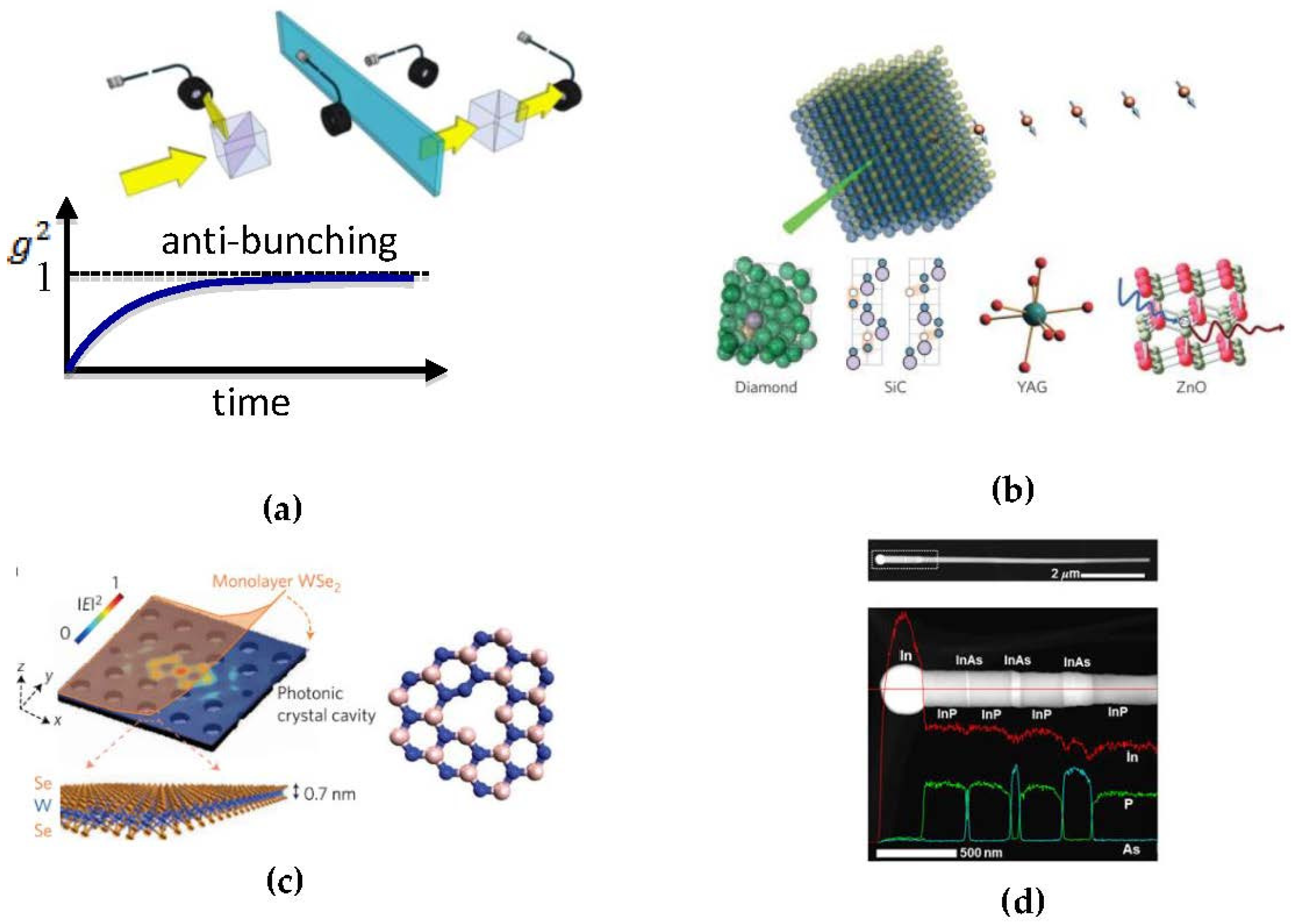
Figure 2.
(a) Temperature-dependent photoluminescence spectra of PbS QDs (quantum dots) excited with 980 nm continuous wave laser diode. (b) Unnormalized second order intensity autocorrelations from a single PbS/CdS nanocrystal and PbS/CdS cluster. (c) Cathodoluminescence spectra of an InP/InAs NW at 8 K; (d) SEM image of an InP/InAs NW, schematic diagram of the NW structure and monochromatic cathodoluminescence images of the NW at different wavelengths; (e) Photoluminescence spectrum and (f) time-resolved photoluminescence at 4 K of an InAs/InP QD grown by metalorganic vapor phase epitaxy. Figures reproduced from (a) Birowosuto, M.D., et al. Opt. Commun. 2017, 383, 555–560. Copyright 2017 by Elsevier B.V.; (b) Correa, R.E., et al. Nano Lett. 2012, 12, 2953–2958. Copyright 2012 by American Chemical Society; (c,d) Guoqiang, Z., et al. Nanotechnology 2015, 26, 115704. Copyright 2015 by IOP Publishing; (e,f) Birowosuto, M.D., et al. Sci. Rep. 2012, 2, 321. Copyright 2012 by Springer Nature.
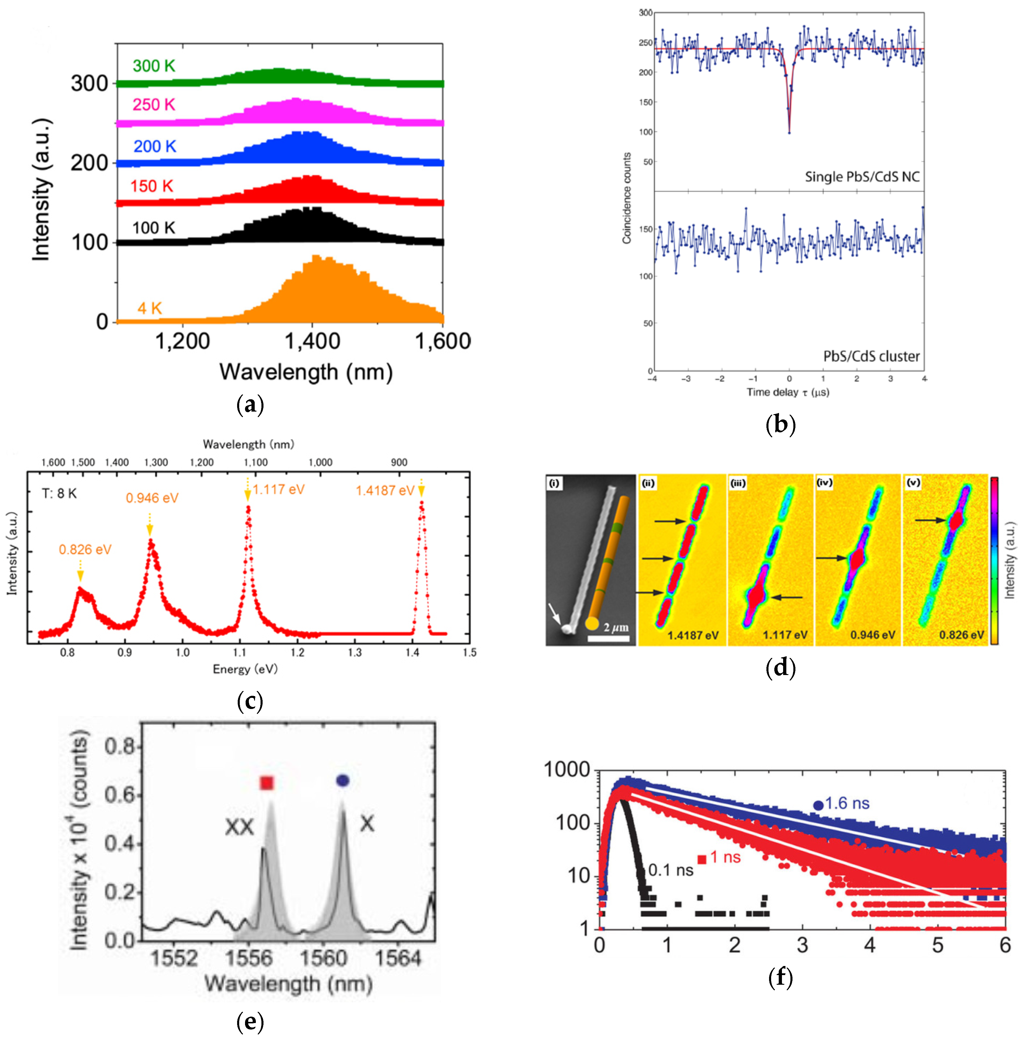
Figure 3.
(a) Emission spectra of hBN monolayer and multilayers and (b) excitation and emission polarization curves of a single defect in hBN multilayer created by electron beam irradiation. (c) Photoluminescence (PL) intensity mapping of laser irradiated regions in hBN flakes. Inset: a typical PL spectrum taken from the bright spot. (d) Second order autocorrelation function curve from individual color centers in hBN flakes. (e) Emission polarization curve (black balls) with cos2(θ) function fitting (red solid line). The excitation is vertically polarized (blue solid line). Measurements were conducted using a 371 ± 5 nm, 50 mW laser at room temperature. Figures reproduced from (a,b) Tran, T.T., et al. Nat. Nanotechnol. 2015, 11, 37. Copyright 2015 by Springer Nature; (c–e) Songyan, H., et al. 2D Mater. 2018, 5, 015010. Copyright 2018 by IOP Publishing.

Figure 4.
Various types of dielectric environment to control spontaneous emission. (a) CdSe QDs embedded in 3D inverse opal photonic crystals; (b) Fluorescent polystyrene nanospheres embedded in 3D random photonic media of polystyrene (top) and ZnO (bottom); (c) InAs QDs and single ultrathin GaAs layer grown between two 110 nm-thick InP photonic crystal layers; (d) 2D photonic crystal waveguide with 6% engineered disorder; (a,c) are ordered arrays; (b,d) are disordered arrays. Figures reproduced from (a) Lodahl, P., et al. Nature 2004, 430, 654. Copyright 2004 by Springer Nature; (b) Birowosuto, M.D., et al. Phys. Rev. Lett. 2010, 105, 013904. Copyright 2010 by American Physical Society; (c) Birowosuto, M.D., et al. Sci. Rep. 2012, 2, 321. Copyright 2012 by Springer Nature (d) Sapienza, L., et al. Science 2010, 327, 1352. Copyright 2010 by American Association for the Advancement of Science.
Figure 5.
(a) Distribution of the emission rates of dye-spheres for materials with different scattering strengths (1/kl), ZnO (red histogram), polystyrene latex random photonic media (blue histogram) and nonscattering polymer layer (green histogram). (b) Decay rate distributions of fluorescent polystyrene beads on two disordered fractal metal films, isolated gold nanoparticles, and fractal clusters with gold filling fraction of 30% (red histogram) and 82% (blue histogram), respectively. (c) Numerical distributions of the decay rate of fluorescent polystyrene beads for four different systems with the same values of kl = 9.4 and R = 0.63 μ. (d) Characteristic length scale L as a function of kl*. Figures reproduced from (a) Birowosuto, M.D. et al. Phys. Rev. Lett. 2010, 105, 013904. Copyright 2010 by American Physical Society; (b) Krachmalnicoff, V., et al. Phys. Rev. Lett. 2010, 105, 183901. Copyright 2010 by American Physical Society. (c) Sapienza, R., et al. Phys. Rev. Lett. 2011, 106, 163902. Copyright 2011 by American Physical Society. (d) Riboli, F., et al. Phys. Rev. Lett. 2017, 119, 043902. Copyright 2017 by American Physical Society.

Figure 6.
(a) The active region of our sample consists of three InGaAsP quantum wells and is embedded inside a PhC in a 240 nm-thick InP membrane, and (b) their emission rates for different lattice constant samples from 384 to 424 nm; (c) Density plot of PL spectra of a quantum dot in a cavity obtained by scanning temperatures between 4 and 60 K; (d) A movable hybrid cavity and emitter in a photonic crystal and NWs; (e) PL spectra of a single NW on a bare SOI (black lines) and inside the square-grooved waveguide of the photonic crystal (red lines), and (f) details of the cavity spectrum and the green lines show the Lorentzian fits. Figures reproduced from (a,b) Takiguchi, M., et al. Appl. Phys. Lett. 2013, 103, 091113. Copyright 2013 by American Institute of Physics Publishing LLC; (c) Birowosuto, M.D., et al. Sci. Rep. 2012, 2, 321. Copyright 2012 by Springer Nature; (d–f) Birowosuto, M.D., et al. Nat. Mater. 2014, 13, 279. Copyright 2014 by Springer Nature.

© 2018 by the authors. Licensee MDPI, Basel, Switzerland. This article is an open access article distributed under the terms and conditions of the Creative Commons Attribution (CC BY) license (http://creativecommons.org/licenses/by/4.0/).
Share and Cite
MDPI and ACS Style
Diguna, L.J.; Tjahjana, L.; Darma, Y.; Zeng, S.; Wang, H.; Birowosuto, M.D. Light–Matter Interaction of Single Quantum Emitters with Dielectric Nanostructures. Photonics 2018, 5, 14. https://doi.org/10.3390/photonics5020014
AMA Style
Diguna LJ, Tjahjana L, Darma Y, Zeng S, Wang H, Birowosuto MD. Light–Matter Interaction of Single Quantum Emitters with Dielectric Nanostructures. Photonics. 2018; 5(2):14. https://doi.org/10.3390/photonics5020014
Chicago/Turabian StyleDiguna, Lina Jaya, Liliana Tjahjana, Yudi Darma, Shuwen Zeng, Hong Wang, and Muhammad Danang Birowosuto. 2018. "Light–Matter Interaction of Single Quantum Emitters with Dielectric Nanostructures" Photonics 5, no. 2: 14. https://doi.org/10.3390/photonics5020014
Note that from the first issue of 2016, this journal uses article numbers instead of page numbers. See further details here.